I. INTRODUCTION
Multi-Service system is a potential technology for the growth of wireless communication system, such as Global System for Mobile Communications (GSM), Wireless Local Area Network (WLAN), and Worldwide Interoperability for Microwave Access (WiMAX) markets. Reflecting these trends, quad-band bandpass filers (BPFs) were developed and reported to fulfill these applications simultaneously [Reference Studniberg and Eleftheriades1–Reference Wu and Yang4].
In [Reference Studniberg and Eleftheriades1], the authors used two dual-band metamaterial BPFs in parallel to synthesize a quad-band response. However, the design parameters are too complex and the circuit size is large. For further size reduction, a quad-band filter using two stacked dual-mode ring resonators with dual-plane feed was proposed [Reference Liu, Wang, Zeng and Chang2], where the quad-resonant frequencies were created by the fundamental and second harmonic mode within each ring resonator. However, the harmonic to fundamental mode frequency ratio is almost fixed at 2, hence the tuning range is small and the dual-plane structure with defected ground structures (DGSs) process increases cost and complexity. In [Reference Cheng and Yang3], the quad-band filter with stepped impedance resonators (SIRs) and DGSs was proposed to satisfy the specific frequencies applications. However, the ground plane process is still be used and the size shall be further reduced. In [Reference Wu and Yang4], a compact design is achieved by using only two sets of asymmetric SIRs, which show high design freedom to fulfill the specific systems. However, the dimension is still large.
In this paper, we proposed a compact quad-band filter designed based on a novel quad-mode stub-loaded resonator (SLR). By using the embedded stub to control the higher odd mode location, the quad-mode behaviors of the SLR can be achieved with only one resonator, thus the demand of compact dimension can be satisfied by reducing the number of resonators.
II. DESIGN PROCEDURE OF THE QUAD-BAND BPF
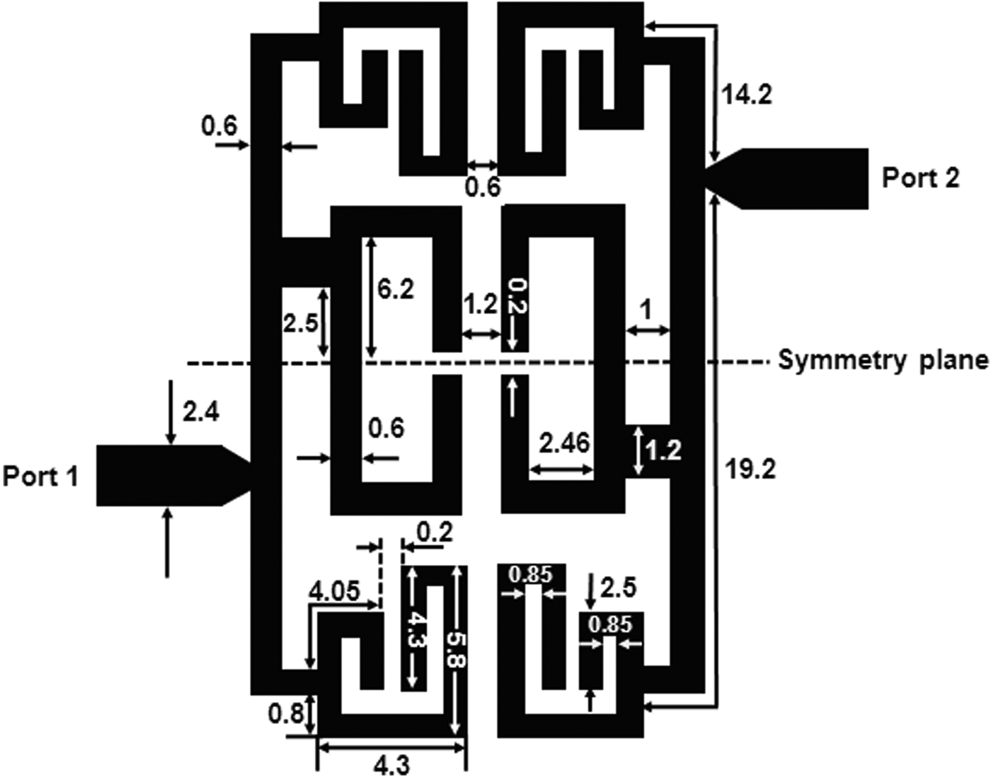
Figure 1 shows the configuration of the proposed quad-band filter. It mainly comprises a 0° feed structure and two embedded uniform half-wavelength resonators used to form a SLR scheme. Thus, the filter size is the same as that of corresponding single-band filter.

Fig. 1. Schematic diagram of the proposed quad-band BPF. (All units in mm).
A) Circuit analysis of the proposed quad-mode resonator by SLR technologies
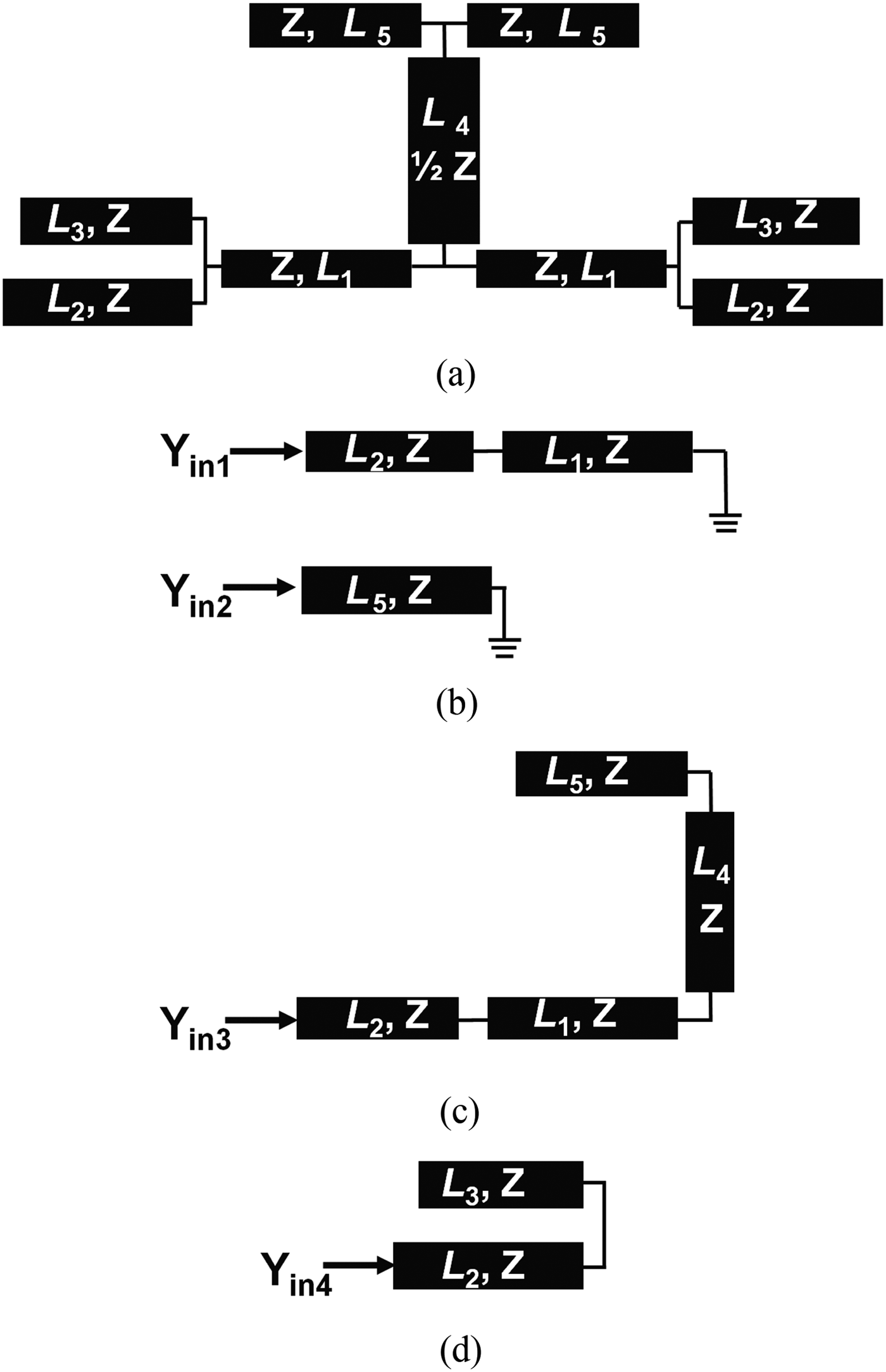
Figure 2(a) shows the quad-mode resonator used in the quad-band application. The physical length of the 0° feed structure is expressed as 2L 5, and the physical length of the embedded uniform half-wavelength resonators are expressed as L 2 + L 3. In addition, the physical lengths of connected microstrip lines are expressed as L 1 and L 4. In this design, the impedance (Z) is set as a constant value (107 Ω) to decrease the difficulty of the design process. The equivalent circuits can be obtained by supposing that symmetry plane become electric wall or magnetic wall, i.e. virtual open or short interface, respectively [Reference Zhang, Chen, Xue and Li5]. For the short condition of the symmetry plane, two odd modes can be obtained when resonating at the physical length of L 2 + L 1 and L 5 respectively as shown in Fig. 2(b). For the open condition of the symmetry plane, an even mode can be obtained when resonating at the physical length of L 5 as shown in Fig. 2(c). In addition, an additional resonant mode as the fourth mode can be created when resonating at the embedded uniform half-wavelength resonator (L 2 + L 3) as shown in Fig. 2(d). It is noted that this half-wavelength resonator is regarded as a SLR. These four modes can illustrate the characteristic of the proposed quad-mode resonator and their frequencies are assigned as f 01, f 02, f 03, and f 04. In this design, the four passband center frequencies at 1.8, 2.4, 3.5, and 5.2 GHz for the quad-band application.
Fig. 2. (a) The primary layout of the proposed quad-mode resonator based on SLR scheme and corresponding equivalent circuits of the (b) odd resonating modes, (c) even resonating mode, and (d) extra resonating mode creating by stub L 3.
B) Resonant frequencies decision of quad-mode SLR
Based on the equivalent circuits shown in Fig. 2(b), the input admittance for the odd-mode circuit 1 (Y in1) and the odd-mode circuit 2 (Y in2) are expressed as:
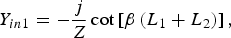 $${Y_{in1}}=- \displaystyle{j \over Z}\cot \left[{\beta \left({{L_1}+{L_2}} \right)} \right]\comma \;$$
 $${Y_{in2}}=- \displaystyle{j \over Z}\cot \left({\beta {L_5}} \right).$$
The resonant conditions for odd-mode circuits 1 and 2 are Y in1 = 0 and Y in2 = 0, respectively. Thus, the first band at f 01 and third band at f 03 can be obtained when the resonant conditions of the odd-mode circuits 1 and 2 are satisfied, respectively.
In Fig. 2(c), ignoring the discontinuity of the folded section, the input admittance Y in3 for even-mode can be approximately obtained as:
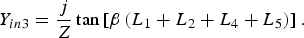 $${Y_{in3}}=\displaystyle{j \over Z}\tan \left[{\beta \left({{L_1}+{L_2}+{L_4}+{L_5}} \right)} \right].$$
When the resonance condition Y in3 = 0 is achieved, the resonant frequency at f 02 can be obtained.
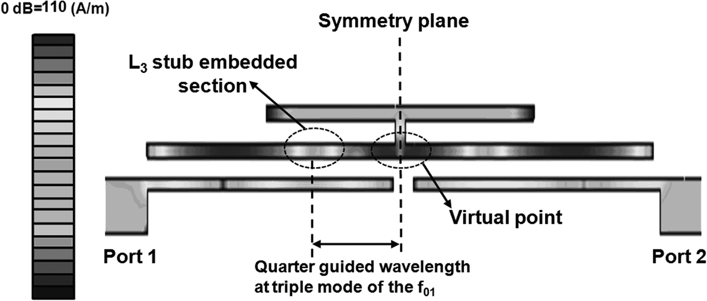
For satisfying the quad-band application, the fourth mode of the embedded uniform half-wavelength resonator is utilized to achieve the fourth passband at f 04. The tuning mechanism is illustrated by using current distribution of the proposed resonator structure without the stub L 3, as shown in Fig. 3. The current distribution under the fourth mode condition shows that the virtual ground point at the symmetry plane, which will turn to open at the location away from the virtual ground point with the distance of quarter guided-wavelength at f 01. Therefore, embedding stub L 3 in this section can form a resonator with a physical length of L 2 + L 3, and its resonance condition is Y in4 = 0, where Y in4 is expressed as:
 $${Y_{in4}}=\displaystyle{j \over Z}\tan \left[{\beta \left({{L_2}+{L_3}} \right)} \right].$$
Based on equation (3), the fourth passband (f 04) can be shifted independently without varying the other passbands when tuning the physical length of L 3. This can be used to extend the design of degree of freedom.
Fig. 3. Current distribution of the quad-mode resonator at triple mode of 1.8 GHz and the function of the embedded stub L 3 in quad-band application.
Therefore, in this study, the design procedure for the proposed quad-band BPF can be expressed as following. Firstly, the first and third passband frequencies (f 01 and f 03) are selected, and then proper physical lengths of L 1, L 2, and L 5 are obtained. Secondly, the physical length of L 4 is used to shift the second passband frequency (f 02) to proper location without varying the first and third passband frequencies (f 01 and f 03). Finally, the physical length of L 3 is used to shift the fourth passband frequency (f 04) to proper location without varying the first, second, and third passband frequencies (f 01, f 02, and f 03).
C) The filter design methodology
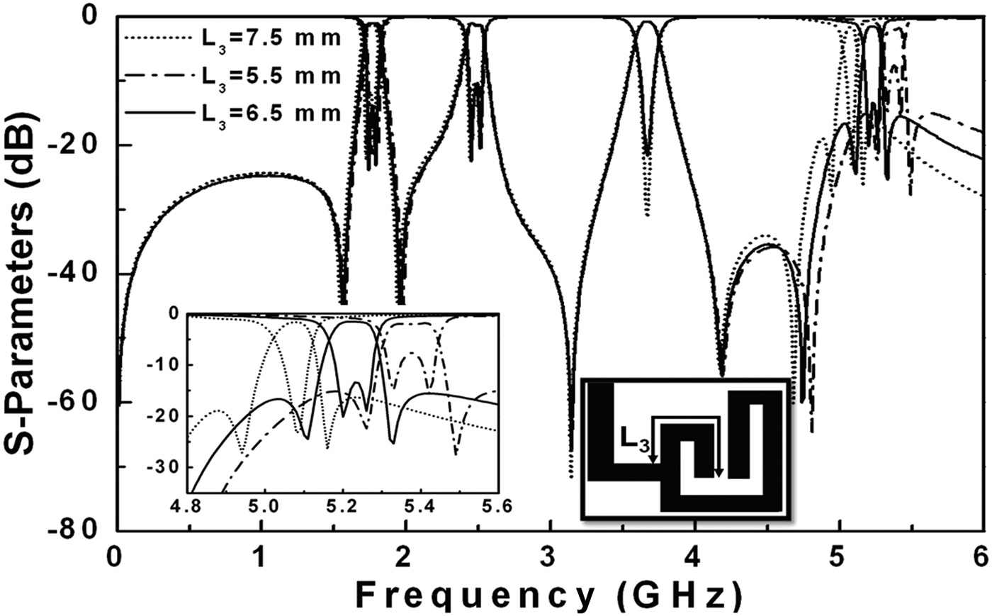
The primary filter topology is then formed by using the proposed SLR structure with the uniform impedance resonator to achieve a compact dimension requirement. In addition, the 0° feed structure of the tapped input/output (I/O) microstrip lines is employed to result in a pair of transmission zeros near each passband edge, based on the theoretical analysis reported in [Reference Tsai, Lee and Tsai6]. Figure 4 shows the simulated frequency response and the primary layouts of the proposed filter versus different embedded stub length L 3. By combining the four resonating circuits as the proposed quad-mode resonator, the quad-mode response can be obtained without changing the resonating frequencies locations. It is clearly verified, as shown in Fig. 4, only the mode frequencies at f 04 can be shifted by changing the length of L 3, whereas the other three resonant frequencies are unchanged. Furthermore, the transmission zero is located at the fourth passband because of the cross-coupling effect [Reference Hong and Lancaster7] between the two resonators responsible for the fourth passband, thus the passband selectivity is enhanced.
Fig. 4. The simulated frequency responses of the proposed filter for 1.8, 2.4, 3.5, and 5.2 GHz, respectively, versus different embedded structural parameters L 3.
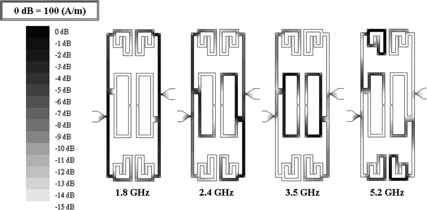
Figure 5 shows the current distributions of the proposed filter at 1.8, 2.4, 3.5, and 5.2 GHz. Though the plots, we can further verify that the electromagnetic (EM) waves are transmitted in the filter from port 1 to port 2 through their corresponding resonant paths.
Fig. 5. Current distributions of the proposed filter at 1.8, 2.4, 3.5, and 5.2 GHz.
D) Bandwidth decision of each passband
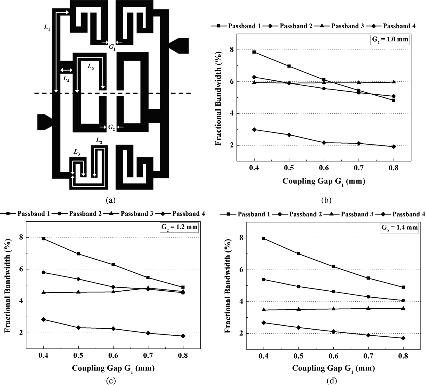
Owing to the adoption of coupling structure, a fractional bandwidth (FBW) of each passband can be decided in accordance with the coupling energy between the resonators. Therefore, two coupling gaps (G 1 and G 2) are used to obtain a proper coupling energy and FBW as shown in Fig. 6(a). The FBW is determined based on the operated frequencies of each passband, and can be expressed as [Reference Hong and Lancaster7]:
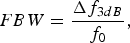 $$FBW=\displaystyle{{\Delta {f_{3 dB}}} \over {{f_0}}}\comma \;$$
where f 0 is the center frequency for each passband, and Δf 3dB is the frequency bandwidth with 3 dB attenuation of coupling energy. Figures 6(b)–6(d) show the FBW with different coupling gaps (G 1 and G 2) by using EM simulator. Obviously, when the coupling gaps (G 1 and G 2) decrease, a strong coupling energy is obtained and then a wider FBW is excited. By mapping Figs 6(b)–6(d), the coupling gaps are decided as 0.6 mm (G 1) and 1.2 mm (G 2) consequently with the FBW of 6.2, 4.9, 4.6, and 2.2% for the four passbands.
Fig. 6. Simulated FBW versus distinct coupling gap (G 1). (a) Geometrical structure of the coupling resonator. (b) Coupling gap (G 2) is fixed as 1.0 mm, (c) 1.2 mm, and (d) 1.4 mm (L 1 = 17.5 mm, L 2 = 15.5 mm, L 3 = 7.1 mm, L 4 = 1 mm, and L 5 = 16.9 mm).
III. EXPERIMENTAL RESULTS AND DISCUSSION
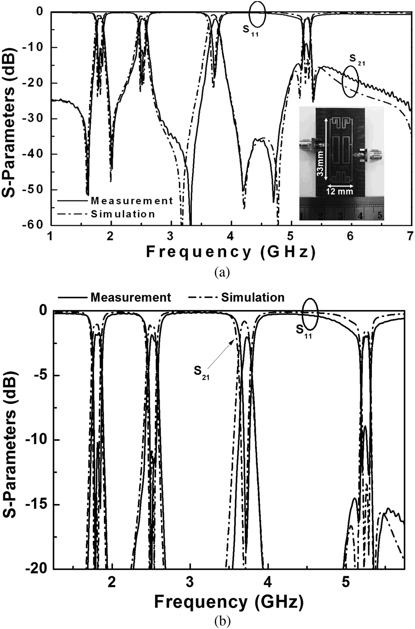
The designed quad-band BPF filter was realized on RT/Duroid 5880 substrate, which has a dielectric constant of εr = 2.2, a loss tangent of 0.0009 and a thickness h of 0.787 mm. The full-wave EM simulator was used for simulation work [8]. Frequency response of the BPF was characterized by an HP8510C Network Analyzer. Figure 7 shows the simulated and measured frequency responses of the fabricated filter and its photograph. The measured insertion losses are 1.7/1.86/2.3/2 dB, and measured return losses are larger than 18/20.5/18/13.7 dB at 1.8, 2.4, 3.5, and 5.2 GHz, respectively. Owing to the 0° feed structure and multi-coupling paths, transmission zeros at 1.6, 2.0, 3.3, 4.2, and 4.7 GHz are clearly observed. In addition, a pair of transmission zeros at 5.16 and 5.37 GHz created by the cross-coupling, resulting in high skirt selectivity. The performances of the measured results are closely matched with the simulated results. Table 1 summarized the comparisons of the proposed filter with other reported quad-band filters [Reference Studniberg and Eleftheriades1–Reference Wu and Yang4]. Comparing to the others, the proposed filter shows more advantages of a most compact size, and easy fabrication without via-hole and multi-layered fabrication processes.
Fig. 7. (a) Simulated and experimental results for the proposed quad-band BPF. Insert is photograph of the fabricated BPF. (b) Performance of each passband in detail.
Table 1. Comparisons with other proposed quad-band filters. (λg is the guiding-wavelength of the center at first passband frequency.)
IV. CONCLUSION
We have designed and fabricated a compact quad-band microstrip BPF for Global System for GSM, WLAN, and WiMAX applications based on a quad-mode SLR. The SLR equivalent circuit consists of one even mode and two odd resonant modes, used to create passbands operated at 1.8, 2.4, and 3.5 GHz. The passband at 5.2 GHz is created by tuning the higher-order mode achieved by the uniform impedance line without using the SIRs. Furthermore, the 0° feed structures and cross-coupling are used to set transmission zeros on each side of each passband, resulting in high skirt selectivity. The superior features indicate that the proposed filter has a potential to be utilized in modern multi-service wireless communication systems.
 Siang-Wen Lan was born in Kaohsiung, Taiwan, in 1988. He received the B.S. and M.S. degrees in Electrical Engineering from the National University of Tainan, Tainan, Taiwan, in 2010 and 2012, respectively. His research interests include the design and fabrication of RF passive/active circuits, VLSI design, and analog IC design.
Min-Hang Weng (M'04) was born in Kaohsiung, Taiwan, in 1971. He received the B.S., M.S., and Ph.D. degrees in Electrical Engineering from the National Cheng-Kung University, Tainan, Taiwan, in 1994, 1996, and 2000, respectively. His research interests include the design and fabrication of RF passive and active circuits, and solar cells.
Chang-Sin Ye was born in Kaohsiung, Taiwan, in 1983. He received the M.S. degree in Electrical Engineering from the National University of Tainan, Tainan, Taiwan, in 2007 and the Ph.D. degree from the National Cheng-Kung University, Tainan, Taiwan, in 2012. His research interests include the design and fabrication of RF passive/active circuits, VHF plasma chamber.
Cheng-Yuan Hung was born in Pingtung, Taiwan, in 1980. He received the M.S. degree in Computer and Communication Engineering from Shu-Te University, Kaohsiung, Taiwan, in 2004 and the Ph.D. degree from the National Cheng-Kung University, Tainan, Taiwan, in 2007. His research interests include the design and fabrication of RF integrated passive and active circuits.