I. INTRODUCTION
Low cost, low profile and ease of fabrication using standard procedures, such as the printed-circuit-board (PCB) techniques, along with easy integration with other planar circuits are making the substrate integrated waveguide (SIW) technology a promising candidate for microwave and millimeter-wave applications. Firstly as proposed in [Reference Hirokawa and Ando1], the SIW technology has been applied to design numerous structures, including power dividers/combiners [Reference Jin and Wen2], directional couplers [Reference Chen, Hao, Li and Wu3], oscillators [Reference Cassivi and Wu4], power amplifier [Reference Abdolhamidi and Shahabadi5], slot array antennas [Reference Yan, Hong, Hua, Chen, Wu and Cui6], and etc. One of the most popular classes of the SIW-based antennas is slot antennas/arrays [Reference Yan, Hong, Hua, Chen, Wu and Cui6, Reference Bayderkhani, Forooraghi and Abbasi-arand7]. Over the years, SIW slot antennas along with other SIW-based components have been designed and analyzed using approximate analytical methods based on transmission-line theory [Reference Kishihara, Yamane and Ohta8], the equivalent-waveguide-width model [Reference Deslandes, Perregrini, Arcioni, Bressan, Wu and Conciauro9], two-dimensional, multi-port methods [Reference Abaei, Mehrshahi, Amendola, Arnieri and Shamsafar10] or finite-element (FEM), and finite-difference (FD) based commercial full wave solvers. The former approach has been computationally efficient, but it does not guarantee the accuracy of the final design results. The latter approach can be time consuming and memory demanding for large structures. However, to investigate a general substrate integrated waveguide antenna, an efficient full-wave analysis is required. For these reasons, the general, efficient, and fast analysis of SIW devices and antennas becomes a new challenge that is the object of intense research in the last few years. A rigorous and efficient full-wave analysis of non-radiating SIW devices based on the dyadic Green's function technique is firstly introduced in [Reference Arnieri and Amendola11, Reference Amendola, Arnieri and Boccla12]. The same approach was extended to efficiently analyze the large single-layer [Reference Arnieri and Amendola13]/multilayer [Reference Casaletti, Valerio, Seljan, Ettorre and Sauleau14] SIW-based slot antenna array with the beam forming network. However, the design and analysis of the SIW-based slot antennas/arrays, considering the radome effects has not been considered.
In practice, to protect the antenna from a variety of environmental effects, a dielectric radome is always covered in front of the antenna. The presence of a radome can affect the gain, beam width, side lobe level and direction of boresight as well as change the voltage standing wave ratio (VSWR) and input impedance of the antenna. These effects in higher frequencies are more critical. Thus, the ability to accurately predict the effect of a radome on the operation of an antenna in the design process is more desirable. There are many instances in literature discussing the methods for analyzing the dielectric radomes using various numerical approaches [Reference Gao and Felsen15–Reference Meng and Dou18]. However, it seems that in all the above analysis done on the modeling of radomes, the forward decoupling between the antenna and radome was assumed, but a drawback of this decoupling is that reverse coupling from the radome to the antenna was ignored. On the other hand, all the aforementioned methods only focus on the analysis of the radomes and the effects of radome on the VSWR but aperture distribution of the antennas are not considered.
Motivated by the aforementioned issues, in this paper a fast and efficient full-wave analysis of a double-layered SIW-based slot antenna/array radiating into a dielectric slab radome is introduced. The approach of [Reference Arnieri and Amendola13] has been extended to analyze a double-layered SIW slot antenna/array with arbitrary number of radiating and/or coupling slots. In addition, to account the effects of radome on the SIW antenna, the dielectric slab is analyzed using Ray/PO technique. Finally, the equations with the unknowns are solved to obtain the equivalent surface currents on the aperture of slots. To validate the proposed method, the aforementioned theory is applied to a double layered SIW-based cavity backed slot antenna, that was recently proposed in [Reference Bayderkhani, Forooraghi and Abbasi-arand7], radiating into a thick dielectric slab radome. A comparison between proposed method results and finite element simulations are presented and discussed. The results show that the proposed method is both accurate and efficient.
II. OVERVIEW OF THE HYBRID METHOD
As noted in the introduction, the proposed hybrid method combines the method of moment (MoM) and Ray/physical optics (PO) technique to analyze the double-layered SIW-based slot antenna radiating into a dielectric stacked radome. (The extension of the formulation to the multilayered case is straightforward and will not be explicated here.) In the proposed hybrid method, the domain of solution is divided into two parts: the high frequency part placed away from the antenna (PO region) including a dielectric stacked radome and low frequency part (MoM region) including a double-layered SIW-based slot antenna (see Fig. 1).

Fig. 1. Stacked-PPW geometry analyzed. A radome shell is located on the top wall of the antenna.
The MoM along with mode matching technique is used to treat the double-layered SIW-based slot antenna (internal region). This is done by representing the field in the post walled structure through the dyadic Green's function of the parallel plate waveguide [Reference Arnieri and Amendola11]. Additionally, to analyze the external region, the PO method is employed in conjunction with ray principles to model the field transmission and reflection through the stacked radome's wall. To do so, the equivalence principle is applied on the radome's surface and the forward as well as backward radiation is calculated. The total field in the external region is then obtained by the summation of incident fields impinging from the antenna and scattered fields from the radome. Then the surface integration equation is established on the aperture of slots. Finally, the equations with the unknowns are solved to obtain the equivalent surface currents on the aperture of slots. Consequently, the number of unknowns is given by the number of modes assumed in each slot (Np) multiplied by the number of slots (NS) i.e. N p × N s. As a result, the computational efficiency is achieved along with reasonable accuracy using the proposed hybrid method. It should be noted that in spite of pervious researches done for modeling the dielectric radomes, in the application of surface equivalence principle, the effects of back radiation on the antenna aperture distribution and input impedance of the antenna are also accounted. This hybridization of the two techniques is described in detail in Section III.
Given the above presuppositions, the implementation of the proposed hybrid method is as follows:
(1) First the problem is divided into two equivalent sub-problems, (i) MoM region and (ii) PO region.
(2) In MoM region: invoking the field-equivalence principle, the slots are replaced by a metal plate with the equivalent magnetic currents Minner = M and Mouter = −M located onto their respective surfaces.
(3) The unknown magnetic currents M is discretized as a sum of suitable basis functions.
(4) In the PO region: the antenna fields are computed on the radome's surface for each mode of basis function of the radiating slots. These fields are then used as the excitation for the PO treatment of the radome.
(5) PO currents are computed on the inner and outer side of radome's wall. The PO currents are then used as the external source radiating into the free space and antenna aperture.
(6) Invoking the pre-computed PO currents as excitation, a MoM system is generated to find the MoM equivalent currents on the aperture of slots.
(7) The MoM matrix is finally solved and the equivalent currents are determined.
The above steps are discussed below in more detail.
III. PROBLEM FORMULATION
Invoking the surface equivalence principle the original problem is divided into the simpler sub-problems: (i) in MoM region: the slots are short-circuited and the equivalent magnetic currents Minner = M and Mouter = −M are introduced onto their respective surfaces: (ii) in PO region: the equivalent magnetic currents are located on the radome's surface as shown in Fig. 1.
There are two sets of current to consider. The first set is the currents in the MoM region on the aperture of slots. The second set refers to the currents in the PO region on the surface of the radome. To avoid ambiguity the subscripts MM and PO are used to denote the MoM region and the PO region, respectively. In the next sub-sections the detailed analysis of the MoM–PO approach will be discussed.
A) PO region modeling
The PO method is a high frequency technique and appropriate for analyzing the electrically smooth-radii radome efficiently, where the assumption of locally flat surface can be invoked. The PO calculates the surface currents induced on metallic or dielectric surfaces due to an incident electromagnetic field [Reference Harrington19]. Thus, in our formulation, the PO method is exploited to analyze the flat dielectric radome, where due to the flatness of the radome surface, the assumption of locally flat surface is satisfied. Based on PO, the equivalent magnetic currents are expressed as the total fields on the internal and external radome surfaces. Thus, the equivalent magnetic current induced on inner and outer surface of radome for qth modes of the jth radiating slot is obtained by
 $$M_{inner\comma\, q\comma\, j}^{PO}=\lpar {\mathop{E}\limits^{\frown}}^i_{q\comma\,j} + {\mathop{E}\limits^{\frown}}_{q\comma\,j}^r \rpar \times {\mathop{n}\limits^{\frown}} _{1}\comma \; $$
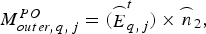 $$M_{outer\comma\, q\comma\, j}^{PO}=\lpar {\mathop{E}\limits^{\frown}}_{q\comma\,j}^t \rpar \times {\mathop{n}\limits^{\frown}}_{2}{\comma \;} $$
where  ${\mathop{n}\limits^{\frown}} _{1} $ and
  ${\mathop{n}\limits^{\frown}} _{2} $ are the unit normals depicted in Fig. 1. It should be noted that, in our case
  ${\mathop{n}\limits^{\frown}}_{1}=- {\mathop{n}\limits^{\frown}}_{2} $; Also,
  ${\mathop{E}\limits^{\frown}}^i $,
  ${\mathop{E}\limits^{\frown}}^r $ and
  ${\mathop{E}\limits^{\frown}}^t $ refer to the incident, reflected and transmitted fields, respectively. The incident field,
  ${\mathop{E}\limits^{\frown}}^i _{q\comma\, j} $, is radiated by qth modes of the jth radiating (not coupling) slots and evaluated in the inner surface of radome. The reflected fields
  ${\mathop{E}\limits^{\frown}}^r _{q\comma\, j} $ as well as transmitted ones
  ${\mathop{E}\limits^{\frown}}^t _{q\comma\, j} $ are evaluated using ray optics principle. They are given by:
 $$\eqalign{& {\mathop{E}\limits^{\frown}}_{r} = \lpar {\mathop{E}\limits^{\frown}}_{i}. {\mathop{v}\limits^{\frown}}_{\bot}^i \rpar R_{\bot} {\mathop{v}\limits^{\frown}}_{\bot}^r + \lpar {\mathop{E}\limits^{\frown}}_{i}. {\mathop{v}\limits^{\frown}}_{\vert \vert}^i \rpar R_{\vert \vert } {\mathop{v}\limits^{\frown}}_{\vert \vert}^r \comma \; \cr & {\mathop{E}\limits^{\frown}}_{t} = \lpar {\mathop{E}\limits^{\frown}}_{i}. {\mathop{v}\limits^{\frown}}_{\bot}^i \rpar T_{\bot} {\mathop{v}\limits^{\frown}}_{\bot}^t + \lpar {\mathop{E}\limits^{\frown}}_i. {\mathop{v}\limits^{\frown}}_{\vert \vert}^i \rpar T_{\vert \vert} {\mathop{v}\limits^{\frown}}_{\vert \vert}^t\comma \;} $$
where
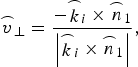 $${\mathop{v}\limits^{\frown}} _ {\bot} = \displaystyle{ - {\mathop{k}\limits^{\frown}}_i \times {\mathop{n}\limits^{\frown}}_{1} \over \left\vert{\mathop{k}\limits^{\frown}}_{i} \times {\mathop{n}\limits^{\frown}} _{1} \right\vert}\comma \; $$
 $$\eqalign{& {\mathop{v}\limits^{\frown}}_{\vert \vert}^i = {\mathop{v}\limits^{\frown}}_{\bot} \times {\mathop{k}\limits^{\frown}}_i\comma \; \cr & {\mathop{v}\limits^{\frown}}_{\vert \vert}^r = {\mathop{v}\limits^{\frown}}_{\bot} \times {\mathop{k}\limits^{\frown}}_r\comma \; \cr & {\mathop{v}\limits^{\frown}}_{\vert \vert}^t = {\mathop{v}\limits^{\frown}}_{\bot} \times {\mathop{k}\limits^{\frown}}_t\comma \;} $$
 ${\mathop{k}\limits^{\frown}}_{i}$ is the propagation direction of the incident wave and
 $$\eqalign{& {\mathop{k}\limits^{\frown}}_{r}=- \cos \lpar 2\theta _i \rpar {\mathop{k}\limits^{\frown}} _{i}+\cos \lpar \theta _i \rpar {\mathop{n}\limits^{\frown}} _{1}\comma \; \cr & {\mathop{k}\limits^{\frown}} _{t}=\cos \lpar \theta _i - \theta _t \rpar {\mathop{k}\limits^{\frown}} _i - \cos \lpar \theta _t \rpar {\mathop{n}\limits^{\frown}} _{1}\comma \; \cr & \cos \lpar \theta _i \rpar ={\mathop{n}\limits^{\frown}}_{1}.{\mathop{k}\limits^{\frown}}\comma \; _i } $$
where θ t is the angle of refraction and can be determined by Snell's law.  $R_ \bot $,
  $R_{\vert \vert } $,
  $T_ {\bot} $ and
  $T_{\vert \vert } $ are the reflection and transmission coefficients for the perpendicular and parallel polarization and are given by [Reference Ishimaru20]
 $$\eqalign{& R_ \bot=\displaystyle{{Z_0 \cos \theta _i - Z_d \cos \theta _t } \over {Z_0 \cos \theta _i+Z_d \cos \theta _t }}\comma \; \quad \quad \quad R_{\vert \vert }=\displaystyle{{Z_d \cos \theta _i - Z_0 \cos \theta _t } \over {Z_d \cos \theta _i+Z_0 \cos \theta _t }}\comma \; \cr & T_ \bot=\displaystyle{{2Z_0 \cos \theta _i } \over {Z_0 \cos \theta _i+Z_d \cos \theta _t }}\comma \; \quad \quad \quad T_{\vert \vert }=\displaystyle{{2Z_d \cos \theta _i } \over {Z_d \cos \theta _i+Z_0 \cos \theta _t }}\comma \; } $$
where Z0 is the characteristic impedance of the free space and  $Z_d=Z_0 /\sqrt {\varepsilon _r } $ is the characteristic impedance of the dielectric radome.
As mentioned earlier in Section II, these known PO currents are used as the external sources and affect the antenna field distribution as well as input admittance. These PO currents are next introduced into the MoM matrix to generate the hybrid MoM–PO method. This hybridization along with how these known PO currents affect the MoM matrix are shown in the next sub-section.
B) MoM region modeling
MoM is used for modeling a double-layered SIW antenna including an arbitrary number of radiating/coupling rectangular slots. This antenna radiates into a grounded thick dielectric slab characterized by ε d and μ d. The geometry under consideration is illustrated schematically in Fig. 1. The geometry to be considered here is divided into a three distinct regions: R0, also named as interior region, located at the lowest layer of SIW slot antenna/array and includes a generic SIW circuit with arbitrary number of coupling slots and posts excited through coaxial or waveguide ports; R1 that is the top layer of SIW slot antenna excited by the coupling slots placed on the rear face and radiated into the external region by the slots etched on the top face; and R2 that is the external region away from the antenna containing a grounded thick dielectric slab stacked on the top wall of the antenna and characterized by the constitutive parameters ε d and μ d. The normal vector  $\hat n_{i+1} $ points into the region R i; Bo2 denotes the boundary surface between R1 and R2; and Bo1 is the boundary between R0 and R1. The parallel plates that are forming the SIW structure are assumed to be a perfect-electric conductor with infinitesimal thickness. In addition, the permittivity of dielectric materials is assumed in more general form as a complex value. Only one excitation is assumed in this paper. However, if several feeding ports are present, their effects are superposed.
1) INTEGRAL EQUATION
Using the field-equivalence principle, the slots are replaced by a metal plate and modeled as equivalent magnetic currents M flowing on the inner and -M on the outer surface as shown in Fig. 1. As far as narrow rectangular slots are of interest, it can be assumed that there is only transverse electric fields component across the slots, and the magnetic current is completely directed along the longitudinal direction and its transverse dependence is neglected. Applying the boundary conditions on the aperture of slots requires the tangential electric and magnetic fields to continue. The continuity of magnetic field across the surface S of the slots leads to the following general integral equation for each slot i:
 $${\mathop{n}\limits^{\frown}} \times H_{tot}^{inner} \lpar r\rpar ={\mathop{n}\limits^{\frown}} \times H_{tot}^{outer} \lpar r\rpar $$
 $$\eqalign{& {\mathop{n}\limits^{\frown}} \times \left({H_{inc}^{inner} \lpar r\rpar +\sum\limits_j^{Ns} {H_{M\,\_\,slot\comma\, j}^{inner} \lpar r\rpar } } \right)\comma \; \cr & \quad={\mathop{n}\limits^{\frown}} \times \left(\matrix{H_{inc}^{outer} \lpar r\rpar +\hfill \cr+\sum\limits_j^{Ns} {H_{M\,\_\,slot\comma\, j}^{outer} \lpar r\rpar +\sum\limits_q^{Nq} {\sum\limits_j^{Ns} {H_{j\comma\, q}^{PO} \lpar r\rpar } } } \hfill} \right)r \in S\comma \; _i } $$
in which [Reference Arnieri and Amendola13]
 $$\eqalign{& H_{inc} \lpar r\rpar =- j\omega \varepsilon _0 \varepsilon _r \cr & \quad \quad .\vint\!\!\!\vint\limits_{V_{SRC} } {\bar G_{PPW} \lpar r\comma \; r^{\prime}\rpar } .M_{SRC} \lpar r^{\prime}\rpar dr^{\prime}+H_S^{M_{SRC} } \lpar r\rpar \comma \; } $$
 $$\eqalign{& H_{M\,\_\,slot\comma\, j}^{} \lpar r\rpar =- j\omega \varepsilon _0 \varepsilon _r \cr & \quad \quad .\vint\!\!\!\vint\limits_{S_j } {\bar G_{PPW} \lpar r\comma \; r^{\prime}\rpar } .M_j \lpar r^{\prime}\rpar dr^{\prime}+H_S^{M_j } \lpar r\rpar \comma \; } $$
where r and r′ define the observation and source point, respectively, M j is the equivalent magnetic current source defined on the surface of slot j (S j),  $\bar G_{PPW} \lpar r\comma \; r^{\prime}\rpar $ is the dyadic Green's function of the parallel plate waveguide when all the slots are short-circuited, H MS is the field scattered by the metallic posts due to the current M, both given in Appendix A and B, respectively; M SRC(r′) is the current-source distribution defined in volume V SRC; and H PO is the magnetic field pre-computed by Ray/PO technique modeling the radome effects and has non-zero value only for outer region.
In the application of the above formulas the correct sign of magnetic currents should be assigned carefully because of the possible presence of magnetic currents on both the upper and the lower plates of each PPWs. Due to the opposite directions of the vectors normal to the different interface, they have different sign in integral equation. The equation (9) is the more general form of integral equation and some quantities of (9) may be zero in various regions. Region R0 includes the excitation ports along with coupling slots. Thus in the equation assigned on boundary Bo1, the H PO(r) is zero. However, R1 contains the coupling and radiating slots without excitation ports. Therefore, on the boundary Bo2 (see Fig. 1), in the equation (9) the  $H_{inc}^{inner} \lpar r\rpar $ is zero but because of the presence of PO currents on the radome's surface, H PO(r) is not null. As mentioned earlier, only one excitation source in R0 is assumed. Therefore, in this paper, the
  $H_{inc}^{outer} \lpar r\rpar $is zero in all regions.
2) FORMULATION OF HYBRID MOM–PO METHOD
The equivalent magnetic currents which are used to model the slots are expanded in terms of an entire domain sinusoidal basis function, as shown in Fig. 2. The magnetic currents for a slot j are
Fig. 2. Shape of basis function.
 $$M_j^{MM} \lpar r^{\prime}\rpar ={\mathop{v}\limits^{\frown}} _j \sum\limits_q {f_{q\comma\, j} \lpar r^{\prime}\rpar .V_{q\comma\, j} } \quad \quad 1 \leq j \leq N_s\comma \; $$
 $$f_{q\comma\, j} \lpar r{\rm ^{\prime}}\rpar =\sin\lpar k_q \lpar L_j /2+v_j \rpar \rpar \comma \; \quad {\rm \vert }v_j {\rm \vert } \leq L_j $$
 $$k_q=\displaystyle{{q\pi } \over {L_j }}\quad {\rm and}\quad r{\rm ^{\prime}=\,}r_{jq}+u{\mathop{u}\limits^{\frown}} _j+v{\mathop{v}\limits^{\frown}} _j\comma \; $$
where r jq is the center of the qth basis function on the slot j, V q, j are the unknown expansion coefficients, N s is the number of slots, L j is the length of the jth slot and q spans over the number of modes N q.
Substituting (10)–(14) into the (9) and applying the Galerkin's method, the integral equations can be converted into a system of N s × N q linear equations with N s × N q unknowns
 $$h_{p\comma\, i}=\sum\limits_{q\comma\, j} {Y_{q\comma\, j}^{p\comma\, i} .V_{q\comma\, j} } \quad \quad \forall \lpar p\comma \; i\rpar \comma \; $$
where p and q span over the basis functions, while i and j span, the number of slots, NS.
 $$h_{p\comma\, i}=\left\{{\matrix{ {\vint\!\!\!\vint\limits_{S_i } {f_{p\comma\, i} \hat v_i .H_{inc} \lpar r\rpar {\rm d}r} } & {\matrix{ {{\rm for}} & {{\rm interior \,\,region}} \cr } } \cr 0 & {{\rm other \,\,regions}} \cr } } \right.\comma \; $$
 $$Y_{q\comma j}^{p\comma i}=Y_{q\comma j}^{p\comma i} \lpar {\rm int1}\rpar +Y_{q\comma j}^{p\comma i} \lpar {\rm int2}\rpar +Y_{q\comma j}^{p\comma i} \lpar ext\rpar \comma \; $$
 $$\eqalign{&Y_{q\comma\, j}^{p\comma\, i} \lpar {\rm ext}\rpar \cr & = \matrix{\left\{\matrix{j\omega \varepsilon _0 \varepsilon _d \vint\!\!\!\vint\limits_{S_i} dr\vint\!\!\!\vint\limits_{S_j} dr^{\prime}f_{p\comma\, i} \hat v_i. \bar G_{ext} \lpar r\comma \; r^{\prime}\rpar. \hat v_j\, f_{q\comma\,\, j} + \vint\!\!\!\vint\limits_{S_i } dr f_{p\comma\, i} \hat v_i.H^{PO} \lpar r\rpar\cr 0 \cr {\rm for}\ {\rm radiating} \ {\rm slots} \hfill\cr{\rm otherwise}\hfill } \right. \cr \hfill}\comma } $$
 $$\eqalign{Y_{q\comma j}^{p\comma i} \lpar {\rm int}\rpar & =j\omega \varepsilon _0 \varepsilon _r . \cr & \vint\!\!\!\vint\limits_{S_i } {dr} \vint\!\!\!\vint\limits_{S_j } {dr^{\prime}f_{p\comma i} } \hat v_i .\bar G_{PPW} \lpar r\comma \; r^{\prime}\rpar .\hat v_j f_{q\comma\, j} \cr & \quad +\vint\!\!\!\vint\limits_{S_i } {drf_{p\comma i} \hat v_i } .H_S^{f_{q\comma j} } \lpar r\rpar \comma \; } $$
where  $Y_{q\comma\, j}^{p\comma\, i} \lpar {\rm int1}\rpar $ and
  $Y_{q\comma\, j}^{p\comma\, i} \lpar {\rm int2}\rpar $ are the admittance elements in R0 and R1 regions, respectively and have the same form of (19). In the application of (15) it should be noted that in each region, only corresponding slots should be considered, for example in R0 the radiating slots are vanished. The incident field H inc(r) is defined as the magnetic field radiating into the structure by a port source with short circuited slot. In the above formulation only one port source which is radiated in interior region is assumed. As mentioned before, if several feeding ports are presented, their effects are superposed. The modeling of coaxial as well as waveguide ports radiated in non-radiating SIW structures are explained in [Reference Arnieri and Amendola11], but in this paper for the sake of brevity only the coaxial port is assumed. As is well documented in literature, a coaxial probe with inner radius of a and outer radius of b, is modeled as a ring of magnetic current given by [Reference Harrington19]
 $$M_{SRC} \lpar r^{\prime}\rpar =- {\mathop{\phi}\limits^{\frown}} \displaystyle{V \over {\left\vert {\rho ^{\prime} - \rho _s } \right\vert \ln \lpar {\rm b/a}\rpar }}\delta \lpar z^{\prime}\rpar \comma \; $$
where V is the voltage between the inner and outer conductors, ρ s is the position of the center of the inner conductor and ρ′ is a point inside the annular region where the magnetic current is flowing. As shown previously in [Reference Arnieri and Amendola11], by substituting (20) into the (10), the following expression (21) is obtained.
 $$\eqalign{H_{inc} \lpar r\rpar & =- \displaystyle{{2\pi V} \over {\ln \left({\displaystyle{b \over a}} \right)}}\displaystyle{{\omega \varepsilon } \over {2h}}\sum\limits_m {\left({1 - \displaystyle{{\delta _{m0} } \over 2}} \right)} \displaystyle{1 \over {k_{\rho m}^2 }}\left({\nabla \times {\mathop{z}\limits^{\frown}}} \right)\cos \,\left({k_{zm} z} \right)\cr &\quad \left\{\matrix{H_0^{\lpar 2\rpar } \lpar k_{\rho m} \rho \rpar \left[{J_0 \lpar k_{\rho m} \rho \rpar - J_0 \lpar k_{\rho m} a\rpar } \right]\hfill \cr + J_0 \lpar k_{\rho m} \rho \rpar \left[{H_0^{\lpar 2\rpar } \lpar k_{\rho m} b\rpar - H_0^{\lpar 2\rpar } \lpar k_{\rho m} \rho \rpar } \right]\hfill} \right\}\cr &\quad +\sum\limits_{l=1}^{N_C } {\sum\limits_{n\comma m} {\left({\nabla \times {\mathop{z}\limits^{\frown}}} \right)H_n^{\lpar 2\rpar } \lpar k_{\rho m} \left\vert {\rho - \rho _l } \right\vert \rpar } } . \cr &\quad .\cos \left({k_{zm} z} \right)e^{ - jn\phi _l } A_{m\comma\, n\comma\, l}^M \lpar M_{SRC} \rpar \cr &\quad \phi _l = \angle \left({\rho - \rho _l } \right)\comma \; } $$
where N c is the number of cylinders.
A) Treatment of external region
The kernel of integral relevant to external region is separated into two terms, see the expression (18): (i) the first term models the unknown magnetic currents flowing on the surface of radiating slots and (ii) the second term is relevant to the precomputed PO currents flowing on the inner surface of the radome that takes into account the PO region effects. In fact, the first term of (18) models the condition in which the slots radiate in an infinitely grounded dielectric medium without considering the reflections from the boundary of radome, the second term of (18) models these reflections.
The Green's function of a homogeneous unbounded dielectric region has the following form:
 $$\bar G_{ext} \lpar r\comma \; r^{\prime}\rpar =\left({\bar I+\displaystyle{{\nabla \nabla } \over {k^2 }}} \right)\displaystyle{{e^{ - jk\left\vert {r - r^{\prime}} \right\vert } } \over {2\pi \left\vert {r - r^{\prime}} \right\vert }}\comma \; $$
where 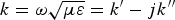 $k=\omega \sqrt {\mu \varepsilon }=k^{\prime} - jk^{\prime \prime} $ is the wave number in the dielectric medium.
In evaluating the first term of  $Y_{q\comma j}^{p\comma\, i} \lpar ext\rpar $ in (18) the singular case will occur when p = q. In this condition the integral can be evaluated by invoking a suitable change of variables, yielding the following expression:
 $$\eqalign{Y_{p\comma i}^{p\comma i} \lpar ext\rpar & =- j\omega \varepsilon _0 \varepsilon _d \displaystyle{1 \over {\pi k^2 }} \cr &\quad .\left[{\vint\limits_0^{\theta _0 } {d\theta \vint\limits_0^{{{L_p } / {\cos \theta }}} {d\rho+\vint\limits_{\theta _0 }^{\pi /2} {d\theta \vint\limits_0^{W_i /\sin \theta } {d\rho } } } } } \right]. \cr &\quad .F_1 \lpar \rho\comma \; \theta \rpar \comma \; } $$
 $$\eqalign{F_1 \lpar \rho\comma \; \theta \rpar & =\lpar W_i - \rho \sin \theta \rpar e^{- jk\rho} \cr &\quad .\left[{\lpar k^2 - k_p^2 \rpar } \right. \lpar L_p - \rho \cos \theta \rpar \cos \lpar k_p \rho \cos \theta \rpar \cr &\quad +\left. {\displaystyle{1 \over {k_p }}\lpar k^2+k_p^2 \rpar \sin \lpar k_p \rho \cos \theta \rpar } \right]\semicolon \; } $$
with θ 0 = tan−1(W i/L p).
The second term of (18) can be easily computed numerically using Gauss quadrature. (In this case the singularity is not occurring due to the fact that the PO current source, which is following on radome's surface, is always away from the unknown magnetic currents of slots.)
B) Treatment of internal region
The internal region of the geometry consists of two regions of R0 and R1 as shown in Figure 1. To evaluate the $Y_{q\comma\, j}^{p\comma\, i} \lpar {\rm int}\rpar $, defined in (19), by assuming the corresponding slots in each region, the integral can be decomposed into two parts: the first part takes into account the parallel plates' contribution and the second one coming from the field scattered by the conducting cylinders.
The parallel plates' contribution can be numerically evaluated using Gauss quadrature for two separate modes. However, the singular case that will occur for p = q can be evaluated using the following expression:
 $$\eqalign{&\hat v.\bar G_{PPW} \lpar r\comma \; r^{\prime}\rpar .\hat v^{\prime}\vert _{\scriptstyle z=z^{\prime}=h \hfill \atop \scriptstyle z=z^{\prime}=2h \hfill} \cr&= \sum\limits_m {\displaystyle{{j\lpar 1 - \displaystyle{{\delta _{m0} } \over 2}\rpar } \over {2k^2\, h}}\left[{k^2 \lpar \hat v.\hat v^{\prime}\rpar - \displaystyle{\partial \over {\partial v}}\displaystyle{\partial \over {\partial v^{\prime}}}} \right]} H_0^{\lpar 2\rpar } \lpar k_{\rho m} \vert \rho - \rho ^{\prime}\vert \rpar \comma \; } $$
where h is the thickness of the PPW. The singularity ρ = ρ′ is easily integrated by adding and subtracting the small argument expression of the Hankel function and using integration by parts [Reference Arnieri and Amendola13].
The scattered field contribution is numerically evaluated using H MS given in Appendix B.
III. VERIFICATION OF RESULTS
To validate the proposed method, the aforementioned theory is applied to a double layered SIW-based cavity backed slot antenna which has recently been proposed in [Reference Bayderkhani, Forooraghi and Abbasi-arand7]. This antenna radiates into a thick dielectric slab radome. A comparison between proposed method results and finite element simulations that are carried out using Ansoft's HFSS are presented and discussed.
A) Input impedance and radiation pattern
The double layered SIW cavity backed slot antenna proposed in [Reference Bayderkhani, Forooraghi and Abbasi-arand7] radiating into a thick dielectric slab radome is considered. The geometry of the antenna-radome system is schematically shown in Fig. 3. Figure 4 shows the SIW cavity backed slot antenna with the corresponding parameters. The SIW antenna structure consists of two main building blocks : the feeding system and the radiating system as shown in Fig. 4. The feeding system and the radiating system are implemented on two different substrate layers.
Fig. 3. Representation of the entire antenna with dielectric radome, the dielectric slab thickness is hr = 2 cm.
Fig. 4. A schematic view of proposed antenna (a) upper substrate including cavity and radiating slots (b) lower substrate including feeding waveguide and coupling aperture.
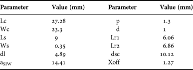
The vertical walls of structure are realized by rows of metalized posts embedded in a dielectric substrate (RO4003TM) with a relative permittivity of 3.55, a loss tangent of 0.0027 and a thickness of 32 mil. The radiating system includes a main cavity, where the radiating slots are etched on the top side of metal as shown in Fig. 3. The cavity is divided into four sub-sections with a radiating slot on the top wall of each sub-section. Also, a feeding short circuited SIW waveguide on the rear side of the cavity excites the cavity by a coupling longitudinal slot. In order to connect two layers a coupling longitudinal slot transition located in common face of two SIW blocks is used as shown in Fig. 3. This antenna radiates into a thick dielectric slab radome with constructive parameters ε d = 2.1 and μ d = 1: the dielectric slab radome stacked on the top wall of the SIW antenna. A coaxial probe is used to excite the antenna. The antenna parameters and corresponding values are listed in Table 1. Figure 5(a) shows the reflection coefficient of the antenna compared with results obtained from HFSS. The phase of the reflection coefficient of the antenna is also depicted in Fig. 5(b). In Fig. 6 the total field pattern of the antenna with radome is illustrated. In addition, the simulated real and imaginary parts of the input impedance of the antenna, using proposed method and HFSS, are shown in Fig. 7. The results indicate that the proposed method is in very good agreement with those obtained from HFSS.
Fig. 5. (a) Magnitude in dB and (b) angle (in degree) of reflection coefficient of the antenna compared with HFSS.
Fig. 6. The total field pattern of the antenna with radome computed by our code and HFSS in y–z plane (the field pattern of the antenna in x–z plane is similar to that in the y–z plane and for the sake of brevity, it is not shown here).
Fig. 7. The simulated real and imaginary parts of the input impedance of the antenna, using our code and HFSS.
Table 1. Antenna parameters and corresponding values.
To show the dielectric radome effects on the input impedance of the antenna, the impedance with and without dielectric slab radome is computed and shown in Fig. 8; from this figure, it can be found that the input impedance of the antenna is strongly altered due to the presence of radome.
Fig. 8 Impact of radome on the input impedance of the antenna.
B) CPU time and storage requirements
The hybrid method described in the present paper requires three matrices to be filled and inverted: in PO region, a matrix should be filled to compute the PO currents on the radome surface; this matrix dimension depends on the number of points assumed to compute the PO currents; in MoM region, two matrices have been filled, one is necessary to evaluate the field scattered by the metallic via holes and the other one to compute the unknown currents with which the slots have been modeled. The size of matrix in PO region depends on the area that is illuminated by the antenna beam and the number of mesh cells which are assumed to cover this area. By increasing the number of mesh cells, the accuracy of the PO fields, and consequently the CPU processing time and memory requirements, are increased. The simulated results indicate that a λ g/10 × /λ g/10 mesh cell size to cover the illuminated area is enough to ensure the accuracy of the calculated PO fields. In MoM region, the size of the two matrices depends on the number of cylinders NC, on the number of slots Ns, and on the substrate thickness, which dictates the number of modes Nz that will be used.
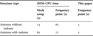
Tables 2 and 3 report the CPU processing time and storage used in simulating the double layered SIW cavity backed slot antenna with radome, respectively.
Table 2. CPU time (Intel Core i7 3.55 GHz, 16 GB RAM)
Table 3. Memory requirement
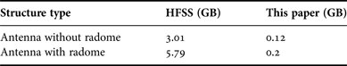
By comparing the CPU time and storage, which was used, it can be found that a considerable saving in time and storage capacity is achieved with respect to HFSS, making it possible to simulate larger structure with limited computing resources with acceptable accuracy. The advantage of the proposed method is more bolder when a complex, multilayered SIW-based antenna radiated into a large (very thick) dielectric radome, is considered. In this case HFSS may be unable to simulate the structure with the computer resources available or the simulation will be more time consuming.
V. CONCLUSION
In this paper, a fast and efficient full-wave method based on a hybrid MoM–PO implementation for the rigorous study of complex, multilayered SIW-based antenna structures, when a dielectric slab radome is located in front of the antenna, have been presented. In addition, the reverse coupling from the radome to the antenna is assumed in spite of pervious works done on the modeling of radomes. The results of the analysis of a double-layered SIW cavity backed slot antenna radiating into a dielectric slab radome using our code were compared to the ones obtained by the commercial FEM-based solver HFSS. The results show a very good agreement, indicating the validity of our approach with an extreme reduction of computational time and storage capacity. The fast calculation feature as well as accuracy of our code makes it suitable for the implementation of optimization techniques for a complex multilayered SIW structure with or without the radome shell.
Reza Bayderkhani was born on February 10, 1985, in Tehran, Iran. He received the B.Sc. degree in electrical engineering, in 2007, and the M.Sc. degree (with honors) in communication engineering, in 2010, both from the Shahed University, Tehran, Iran. He is currently working towards the Ph.D. degree in electrical engineering (communication, field & wave) at the Tarbiat Modares University(TMU). His research interests include computational electromagnetic, planar antenna structures and arrays, and SIW structures.
Keyvan Forooraghi was born in Tehran, Iran. He received the Msc., Technology Licentiate and PhD from Chalmers University of Technology, Gothenburg, Sweden, in 1983, 1988 and 1991 respectively, all in electrical engineering. He was a researcher at the department of network theory during 1992-1993. He joined the department of electrical engineering at Tarbiat Modares University (TMU) in 1993 where he currently is a professor and lectures on electromagnetic, antenna theory and design, and microwave circuits. His research interests include computational electromagnetic, waveguide slot antenna design and microstrip antennas.
Emilio Arnieri was born in Cosenza, Italy, in 1977. He received the degree (with honors) in information technology engineering from the University of Calabria, Rende, Italy, in 2003 and the Ph.D. degree in electronic engineering from the University “Mediterranea” of Reggio Calabria, in 2007. Currently, he is an Assistant Professor with the Dept. of Informatics, Modeling, Electronics and System Engineering(DIMES), University of Calabria (Italy). His main research activities concern the development of dual band antennas and millimeter-wave components, development of numerical methods for the electromagnetic modeling of microwave and millimeter-wave circuits (substrate integrated circuits, slotted substrate integrated waveguide arrays, and substrate integrated waveguide resonators).
Bijan Abbasi Arand received the B.Sc. from the Shiraz University, Shiraz, Iran in 1995 and the M.S. and Ph.D. degrees in Telecommunication engineering from Tarbiat Modares University, Tehran, Iran in 1997 and 2003, respectively.
From 2003 to 2005, He was a researcher of electromagnetic propagation department in Iran Telecommunication Research Center (ITRC).
In 2005, he joined the Satellite communication laboratory of Tarbiat Modares as a Postdoctoral researcher. Since 2010, he is assistant professor in faculty of Electrical and Computer engineering of Tarbiat Modares. He has more than 35 papers and publications in journal and conferences.
APPENDIX A
The dyadic Green's function of the parallel plate waveguide has the following form [Reference Arnieri and Amendola11]:
 $$\eqalign{\bar G_{PPW} \lpar r\comma \; r^{\prime}\rpar & =- \displaystyle{1 \over {k^2 }}\hat z\hat z\delta \lpar r - r^{\prime}\rpar - j\sum\limits_m {\left({1 - \displaystyle{{\delta _{m0} } \over 2}} \right)} \displaystyle{1 \over {2k_{\rho m}^2\, h}} \cr &\quad [\lpar \nabla \times \hat z\rpar \lpar \nabla ^{\prime} \times \hat z\rpar H_0^{\lpar 2\rpar } \lpar k_{\rho m} \left\vert {\rho - \rho ^{\prime}} \right\vert \rpar f_c \lpar k_{zm}\comma \; z\comma \; z^{\prime}\rpar \cr &\quad+\displaystyle{1 \over {k^2 }}\lpar \nabla \times \nabla \times \hat z\rpar \lpar \nabla ^{\prime} \times \nabla ^{\prime} \times \hat z\rpar H_0^{\lpar 2\rpar } \cr &\quad .\lpar k_{\rho m} \left\vert {\rho - \rho ^{\prime}} \right\vert \rpar f_s \lpar k_{zm}\comma \; z\comma \; z^{\prime}\rpar ] \comma \; }$$
with  $k=\omega \sqrt {\mu \varepsilon _0 \varepsilon }$, k zm = mπ/h,
  $k_{\rho m}=\sqrt {k^2 - k_{zm}^2 } $ and
 $$\delta _{m0}=\left\{{\matrix{ {\matrix{ 1 & {for} & {m=0} \cr } } \cr {\matrix{ 0 & {for} & {m \ne 0} \cr } } \cr } } \right.\comma \;$$
 $$f_{c\comma s}=\left({\matrix{ {\cos \lpar k_{zm} z\rpar \cos \lpar k_{zm} z^{\prime}\rpar } \cr {\sin \lpar k_{zm} z\rpar \sin \lpar k_{zm} z^{\prime}\rpar } \cr } } \right.\comma \;$$
where k is the wave number, k zm is the wave number in z direction and k ρm is the radial wave number.
APPENDIX B
H MS is expressed as the series of outgoing cylindrical waves cantered on the metallic cylinders and it has the following form:
 $$\eqalign{H_S^M \lpar r\rpar & =\sum\limits_{l\comma n\comma m} {\nabla \times \left[\matrix{H_n^{\lpar 2\rpar } \lpar k_{\rho m} \vert \rho - \rho _l \vert \rpar e^{ - jn\varphi } \hfill \cr \quad .\cos k_{zm} \lpar h - z\rpar \hat z \hfill} \right]} A_{m\comma n\comma l}^M \lpar M\rpar\hfill \cr &\quad+\sum\limits_{l\comma n\comma m} {\displaystyle{1 \over k}\nabla \times \nabla \times \left[\matrix{H_n^{\lpar 2\rpar } \lpar k_{\rho m} \vert \rho - \rho _l \vert \rpar e^{ - jn\varphi } \hfill \cr \quad .\sin k_{zm} \lpar h - z\rpar \hat z \hfill} \right]} A_{m\comma n\comma l}^N \lpar M\rpar \cr &\quad \varphi=\angle \lpar \rho - \rho _l \rpar .}$$
In (B.1), m spans the number of vertical modes, and spans the number of radial modes, l spans the number of cylinders, and ρ l is the position of the center of the cylinder l. Enforcing the boundary conditions on the metallic posts yield the scattering amplitudes,  $A_{m\comma n\comma l}^M $ (TM mode) and
  $A_{m\comma n\comma l}^N $ (TE mode) [Reference Arnieri and Amendola11].