


I. INTRODUCTION
The information society is rapidly approaching a convergence between communication, multimedia, and computing with the goal of a broad connection of every standard and network at any time and any place. In this framework, several kinds of wireless networks have to be interconnected to suit the user needs [Reference Castello1]. To operate in an effective and transparent way between different wireless access systems the mobile terminal must be able to connect itself to different networks. Because inserting a new stand-alone radio into a mobile handset for each emerging system is not feasible, new multi-band multi-standard terminals are required [Reference Ryynänen, Lindfors, Stadius and Halonen2]. This, in turn, requires a high degree of flexibility in the digital baseband and in the radiofrequency front-end [Reference Ryynänen, Lindfors, Stadius and Halonen2, Reference Desoli and Filippi3]. Moreover, the increasing demand in some wireless communication services requires unfolding the number of frequency bands assigned to a specific service. For instance, the global system for mobile communications operates at both 900 and 1800 MHz bands and wireless local-area networks (WLAN) operate at 2.45 GHz but also at Industrial, Scientific and Medical (ISM) 5 GHz bands.
In this context, dual-band filter structures are emerging for simultaneous operation in multiple frequency bands in wireless communication systems. A number of topologies for dual-band filters have been proposed so far. Some of them use the stepped-impedance resonator (SIR) [Reference Makimoto and Yamashita4–Reference Morelli, Hunter, Parry and Postoyalko6] to fix its spurious response by adjusting the line characteristic impedances [Reference Mokhtaari, Bornemann and Amari7, Reference Zhang and Sun8]. Other topologies based on the dual-behavior resonator have been proposed [Reference Chang, Jeng and Chen9–Reference Quendo, Rius and Person11]; the dual-behavior resonator consists of two bandstop structures that place two transmission zeros on either side of one pole [Reference Quendo, Rius and Person10]. Other dual-band filters are based on a stub-loaded resonator [Reference Zhang, Chen, Xue and Li12] or on a suitable combination of open-loop ring resonators [Reference Chen and Hsu13]. In addition, within the framework of reconfigurable filters, several recent works propose frequency-tunable dual-band filters based on SIRs, by shunt connecting a variable capacitor at its center [Reference Zhang and Xue14–Reference Girbau, Lázaro, Pérez, Martínez, Pradell and Villarino16]; the concept of tunable SIRs was first proposed in [Reference Kapilevich and Lukjanets17], but applied to monoband filters. This work is an extension of [Reference Girbau, Lázaro, Pérez, Martínez, Pradell and Villarino16]. There, the capacitive-loaded SIR was analyzed in terms of tunability; here, a general analysis of the SIR resonator is done and the capacitively loaded SIR is studied, not only in terms of frequency tunability but also in terms of quality factor of both resonances. In addition, the new tunable dual-band hole resonator is also presented; the hole resonator is a variation of the SIR proposed by the authors in [Reference Girbau, Lázaro, Pérez and Pradell18]. Both resonators are compared and integrated in dual-band tunable filters.
In Section II a general analysis of the SIR resonator is provided, which helps to determine the minimum length condition for its design. In Section III, an in-depth analysis of the capacitive-loaded SIR is done in terms of tuning capability, which leads to a closed-form analytical expression that greatly eases the design of this structure in comparison to the analysis available in the literature to date. Here, a study of the quality factor of both resonances is also provided. The analysis of Section III is extended to the new capacitive-loaded hole resonator in Section IV. It is shown that both the capacitive-loaded SIR and hole resonators are good candidates to obtain structures with wide tuning range. In Section V three frequency-agile dual-band filters are provided, based on the resonators that are proposed and analyzed in this work. Two of these filters are designed to work at the WLAN frequency bands, with the first band fixed at 2.45 GHz and the second band tuned between 5.75 and 5.25 GHz. Finally, conclusions are drawn in Section VI.
II. STEPPED-IMPEDANCE RESONATOR
Figure 1 shows the SIR, a resonator with lines of two different characteristic impedances, Z 1 and Z 2.

Fig. 1. Stepped-impedance resonator.
The input admittance is given by

where Y 2 = 1/Z 2 is the characteristic admittance of the outer line, Y 1 = 1/Z 1 is the characteristic admittance of the central line, and θ2 and θ1 are the electrical lengths of the outer and central lines, respectively. The parameter K is defined as the ratio between characteristic impedances K = Z 2/Z 1. The case K = 1 corresponds to the constant-section uniform half-wavelength resonator. By applying the resonance condition |Y IN,SIR| = 0 in (1), the fundamental and second resonance conditions are obtained, respectively [Reference Makimoto and Yamashita4]:
By applying the fundamental resonance condition (2), the ratio between the total electrical length θT and K can be obtained from:
Derivating (4) with respect to θ1 and equaling to zero, only one physically feasible solution is obtained, K = tan2 θ1, which can be substituted in (2) to obtain θ1 − θ2 = nπ. To derive the minimum resonator length, n = 0 and then θ1 = θ2, which leads to
Here, the ratio between the two first resonance frequencies and their corresponding θs1 and θs2 is (note that when K < 1, f 2/f 1 > 2, while when K > 1, f 2/f 1 < 2)
By using the second resonance condition (3), the following expressions can be obtained, depending on the electrical length that is chosen (either θ1 or θ2):
Two physically feasible solutions are obtained: K = tan2 θ2 for (7a) and 1 = K tan2 θ1 for (7b), and the following expression can be derived for both cases:
From (8) it can be observed that the two electrical lengths cannot be equal. In this case, in order to obtain the minimum resonator length (n = 0) θ1 = θ2 + π/2, being the total length θT = 4θ1 + π. Then, the minimum resonator length for the second resonance condition can be obtained from


Figure 2 shows the comparison between the expressions obtained for the fundamental (5) and second (9) resonance conditions, respectively. For the case K < 1 the fundamental condition minimizes the resonator length. However, for the case K > 1 it can be observed that, when K increases, the total length of the resonator increases up to a point in which a design with the second resonance condition is preferred. Since a value of K higher or lower than 1 is chosen depending on the ratio between the two resonance frequencies, the results concerning total length should be taken into consideration especially for K > 5.83. However, in most real cases K is lower than 5.83 and the best option for the resonator length calculation is the use of the first resonance condition. In addition, many real cases (WLAN is the best example), the ratio f 2/f 1 is higher than 2, and this means that SIR resonators with K < 1 must be used.

Fig. 2. Total resonator length as a function of the ratio between characteristic impedances K for the several resonance conditions: fundamental (– + –) and second (–x– and –o–).
III. CAPACITIVE-LOADED SIR
A) Analysis of the resonance frequencies
Figure 3 shows the capacitive-loaded SIR. The structure consists of the SIR presented in Section II where a capacitor C has been shunt connected at the midpoint; following the conclusions of Section II the case Z 1 > Z 2 is considered. The input admittance of the resonator Y IN is

where Z 3 = 1/jωC = −j|Z 3| is the impedance of the shunt-connected capacitor. The case θ1 = β1l 1 = θ2 = β2l 2 = θ has been considered, following conclusions of Section II, being βi the propagation constant at each line section and l i their respective lengths.

Fig. 3. Capacitive-loaded stepped-impedance resonator.
From (10), the first resonance condition can be obtained (K − tan2θ = 0) and the fundamental resonance frequency is given by

where v 1 is the propagation velocity in line 1. The second resonance is obtained from the numerator of (10), which depends on Z 3 (or C). From now on, we will denote the second resonance frequency obtained (already taking capacitance C into account) as f r. Then, f r = f 2 for C = 0 (6) and f r < f 2 for C ≠ 0. The ratio between resonance frequencies and their corresponding θs1 and θsr can be expressed as

The dependence of f r/f 1 on Z 3 (or C) is obtained numerically solving (12) and is plotted in Fig. 4 for two resonators, one with K = 1 (uniform resonator, which is here considered as a particular case of the SIR) and another with K = 0.56 (SIR). For the case K = 1 the following parameters are used: f 1 = 2.45 GHz, f 2 = 4.9 GHz, and Z 1 = Z 2 = 50 Ω. For the case K = 0.56 the following parameters are considered: f 1 = 2.45 GHz, f 2 = 6 GHz, Z 1 = 60 Ω, and Z 2 = 33.6 Ω. The case K = 0.56 is considered here since it is a good example of K < 1 and thus it will permit to use the resonators in filters for WLAN applications (with f 1 = 2.45 GHz and f 2 tuned between 5.75 and 5.25 GHz).

Fig. 4. Dependence of f r/f 1 on Z 3, obtained by numerically solving (12). Case K = 1 and 0.56.
However, although (12) permits a good understanding of the resonator performance, it does not simplify the resonator design procedure; to this end, an analytical closed-form expression relating C and f r/f 1 is given in (13), which directly relates f 1, f 2, f r, K (Z 1 and Z 2), and C (this expression has been validated in [Reference Girbau, Lázaro, Pérez, Martínez, Pradell and Villarino16]):
By using (13) the procedure to design any capacitive-loaded SIR is very simple in contrast to the procedures proposed in works available in the literature to date [Reference Girbau, Lázaro, Martínez, Masone and Pradell15, Reference Kapilevich and Lukjanets17]. In [Reference Kapilevich and Lukjanets17] an analysis based on the ABCD parameters is provided, leading to complicated expressions which do not make its design straightforward. On the other hand, the authors provide in [Reference Girbau, Lázaro, Martínez, Masone and Pradell15] a numerical approximation. Both works are far from the versatility and simplicity that the closed-form analytical expression (13) provides to the designer. A simple three-step design procedure can now be defined: (1) K is determined by fixing f 1 and f 2, which correspond to the fundamental resonance and the maximum value for the second resonance (case C = 0), respectively. (2) The values of Z 1 and Z 2 are fixed, according to line widths that can be physically fabricated. (3) The tuning range of the resonator is fixed; its limits determine two resonance frequencies f r (f r1 and f r2) which, in turn, determine the two extreme capacities C (C 1 and C 2).
Figure 5 shows a comparison in terms of tuning capability between the capacitive-loaded uniform resonator (K = 1) and the capacitive-loaded SIR. Although the maximum frequency in the capacitive-loaded uniform resonator is 2f 1, this limit can be pushed up by using the capacitive-loaded SIR (K < 1) with the only restriction imposed by physical limitations when it is manufactured. The dual structure for the SIR (K > 1) is also compared, leading to the same limitations as the uniform resonator.

Fig. 5. Comparison in terms of tuning capability between the capacitive-loaded uniform resonator and the capacitive-loaded stepped-impedance resonator with K > 1 and K < 1.
Figure 6 shows a measured capacitive-loaded SIR. All designs in this work have been manufactured on RO4003 substrate, with ɛr = 3.55, thickness t = 0.813 mm, loss tangent tg δ = 0.0027, and metal thickness 17 µm. It has been designed with f 1 = 1.5 GHz and f 2 = 3.5 GHz for C = 0 pF. The design parameters are Z 2 = 28.6 Ω, Z 1 = 45 Ω, K = 0.635, l 2 = 11.60 mm, and l 1 = 12.76 mm. The second resonance can be tuned from 3.5 to 2.4 GHz by varying the shunt capacitance from C = 0 to 2 pF. The first resonance remains absolutely fixed at the nominal design position, independently of the shunt capacitance value.

Fig. 6. Measured capacitive-loaded stepped-impedance resonator.
B) Analysis of the quality factor (Q)
In this section, an analytical model for the quality factor of the capacitive-loaded SIR is presented, where both resonance frequencies are taken into account. It can be extended to the SIR just by considering C = 0 pF. For the first resonance, the midpoint of the resonator is short circuited (see Fig. 7). Then, the unloaded Q of a non-resonant short-circuited section can be determined by [Reference Vizmuller19]
where G and B are the real and imaginary parts of the short-circuited half-resonator input admittance, respectively. Note, that the quality factor at the resonance frequency f 1 can be obtained using (14) and imposing the resonance condition B(f 1) = 0. The derivative of B must be evaluated at the considered resonance frequency and is performed numerically. The input impedance can be obtained from the input impedance of a transmission line of length l 2, characteristic impedance Z 2, and complex propagation constant γ2, loaded with a shorted transmission line of length l 1, characteristic impedance Z 1, and complex propagation constant γ1:
where

Fig. 7. Equivalent circuit for the half-SIR resonator for the first resonance (left) and the second resonance (right).
For the second resonance, at the midpoint of resonator the current is zero (see Fig. 7). Then, the unloaded Q of a non-resonant open-circuited section can also be determined using (14).
The Q at the second resonance f r can be obtained by imposing B(f r) = 0. G and B are the real and imaginary parts of the open-circuited half-resonator input admittance, respectively. The input admittance can be obtained from the input admittance of a transmission line of length l 2, which is loaded with a transmission line of length l 1, loaded in turn with a capacitance C/2:
where
where Y C is the admittance of a lossy capacitor with equivalent series resistance (ESR) and capacitance C/2:
and Y 1 = 1/Z 1 and Y 2 = 1/Z 2 are the characteristic admittances of each transmission line. The quality factor depends on the transmission line loss. The complex propagation constant can be expressed as a function of the attenuation and propagation constants, γi = αi + jβi (i = 1,2). Assuming a low-loss substrate and neglecting radiation loss, the attenuation constant can be split into conductor loss (αci) and dielectric loss (αdi), αi = αci + αdi. In this work, the microstrip models for effective permittivity, characteristic impedance, and losses given in [Reference Misra20] are assumed.
Figure 8 compares the simulated and measured quality factor for the capacitive-loaded SIR resonator shown in Figs 3 and 6. As predicted, the quality factor of the first resonance does not depend on the shunt capacitance. The quality factor of second resonance depends on the value of capacitance and also on the parasitic series resistance (ESR). The exact value of ESR depends on the assembly of the component and its capacitance. Specifically, the C06 capacitor kit from Dielectric Labs is here used, which specifies ESR = 0.47 Ω at 1 GHz for capacitors of 1 pF. A reasonable agreement is obtained between the model and the measured quality factors.

Fig. 8. Unloaded quality factor for the first and second resonances as a function of the shunt capacitance C and several ESR. Comparison to the quality factor of the measured resonator.
Figure 9 shows the quality factor for the first and second resonances for several SIRs with different impedance ratios K (all with Z 2 = 25 Ω), as a function of the shunt capacitance. For capacitors with small ESR, the quality factor increases with the capacitance, reaching a maximum at about 1 pF. This behavior can be explained given that for small capacitance values, its quality factor is very high and line losses are dominant. When the capacitance increases, the second resonance frequency decreases (see Fig. 6), thus decreasing the quality factor of the capacitor, because the quality factor Q c of a capacitor is inversely proportional to the capacitance (Q C = 1/(πf rC ESR), for a capacitor with value C/2), up to a value where the capacitor loss dominates over the line loss. Then, the overall quality factor of the resonator decreases with the capacitance. For higher ESR values a maximum also exists but for smaller capacitance values. As shown in Fig. 10, the quality factor increases with the impedance ratio K for the first resonance. However, for the second resonance, the quality factor is almost constant with K (just a small increase is observed for small capacitances with small ESR).

Fig. 9. Quality factor as a function of the shunt capacitance for different impedance ratios K.
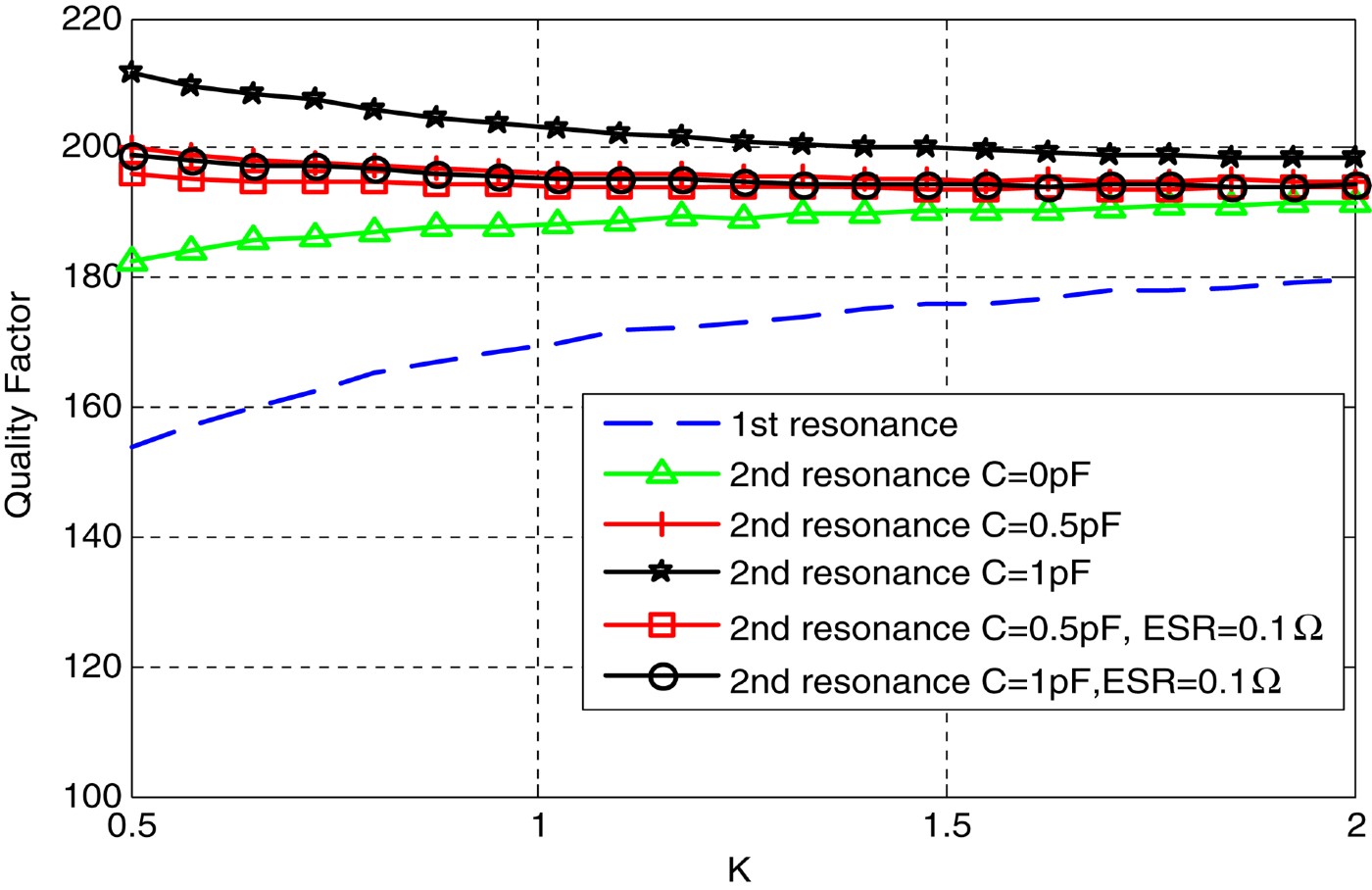
Fig. 10. Quality factor as a function of the impedance ratio K, for different capacitance values and ESR.
IV. CAPACITIVE-LOADED HOLE RESONATOR
In[Reference Girbau, Lázaro, Pérez and Pradell18], the authors have presented a variation of the SIR, referred to as “hole resonator.” The hole resonator is based on a modification of the central line of the SIR structure with K < 1 by which a constant-section resonator is obtained (see the small inset in Fig. 11) while keeping the same features as the SIR. The hole resonator offers some advantages, notably in filters based on parallel-coupled lines. Here in this work the tunable version of the fixed hole resonator is proposed. To this end, the analysis provided in Sections II and III of this paper is still valid and can be applied to this new resonator; however, it must be taken into consideration that now Z 1,HOLE = 2Z 1 (where Z 1,HOLE is the characteristic impedance of each central line of the hole resonator and Z 1 is the characteristic impedance of the central line of the SIR). This assumption is valid whenever the coupling between the two central lines is small. It has been demonstrated in [Reference Girbau, Lázaro, Pérez and Pradell18] that very small couplings, under −30 dB, can be obtained in practical realizations. Then, for this new structure the ratio between impedances K is defined as

Fig. 11. Comparison between a stepped-impedance resonator and a hole resonator.
Figure 11 shows a comparison between a SIR resonator and a hole resonator, both designed for f 1 = 1.25 GHz and f 2 = 3 GHz, with same dimensions, the only difference being in the characteristic impedance of the central lines. It can be shown that they have exactly the same measured behavior. It is also demonstrated that the hole resonator can also be tuned by shunt connecting a capacitor, as shown in Fig. 12. To this end, a narrow line connecting the two central lines at its center has been added for convenience; otherwise, two variable capacitors, one for each central line would be necessary. It can be easily deduced from the symmetry analysis provided in [Reference Girbau, Lázaro, Pérez and Pradell18] for the fixed hole resonator that this line has no effect on its behavior.

Fig. 12. Tuning of the hole resonator by varying the shunt-connected capacitor and comparison with ADS/Momentum co-simulations.
V. TUNABLE DUAL-BAND FILTERS
A) Filters based on the capacitive-loaded SIR
The most typical application of dual-band tunable resonators is dual-band tunable filters; to this end, several filter designs are shown in this section. First, the capacitive-loaded SIR has been integrated in two second-order Chebyshev filters, with K = 1 and 0.56. In order to miniaturize both filters, the resonators have been designed in their open-loop form. Photographs of the manufactured filters are shown in Fig. 13.

Fig. 13. Photographs of the manufactured filters. Tunable dual-band filter with K = 1 (a) and with K = 0.56 (b). (Not to scale.)
The filter with K = 1 (see Fig. 13(a)) has its first pass band at 2.45 GHz and the second at 4.9 GHz. Figure 14 shows the measured insertion and return loss compared to ADS/Momentum™ co-simulation.

Fig. 14. Comparison between measurement and simulation of the tunable dual-band filter with K = 1 (C = 0 pF).
Figure 15 shows the measured frequency tuning range of the filter by varying the shunt-connected capacitance from 0 to 0.5 pF. The maximum design frequency f 2 for this filter is 2f 1 (for C = 0 pF). This limit can be pushed up by using the SIR with K < 1, as it has been demonstrated. A second filter has been designed with f 1 = 2.45 GHz and f 2 = 6 GHz (see Fig. 13(b)). Since f 2 is very far from 2f 1, a dual-band input/output matching network is included. The matching network design is based on a stepped-impedance transmission line (non-synchronous alternating-impedance transformer) [Reference Lee, Chen, Tsai and Tsai21, Reference Tsai, Tsai and Lee22]. The filter measured insertion and return loss are compared to simulation in Fig. 16, showing good agreement. Figure 17 shows its measured tuning range for C between 0 and 0.2 pF.

Fig. 15. Tunable dual-band filter measured response with K = 1 for 0 < C < 0.5 pF, with a measured tuning range between 4.9 and 4.12 GHz, insertion loss between 1.8 and 2.4 dB and relative bandwidth between 8.1 and 6.3%, respectively. The measured first pass band at 2.42 GHz has 0.63 dB insertion loss and 11.5% relative bandwidth.

Fig. 16. Comparison between measurement and simulation of the dual-band filter with K = 0.56 (C = 0 pF).

Fig. 17. Tunable dual-band filter measured response with K = 0.56 for C between 0 and 0.2 pF, with a measured tuning range between 5.97 and 5.45 GHz, insertion loss 2.1 and 2.9 dB, and relative bandwidth 7.2 and 6.1%, respectively. The measured first pass band at 2.47 GHz has 0.83 dB insertion loss and 10.5% relative bandwidth.
A faster degradation in the second band (insertion loss) has been experienced in the case K = 0.56, since it has been proved to be very sensitive to the precision in placing the variable capacitors. It is also important to note that when resonators are integrated into a filter the optimum position for the capacitor is no longer the physical midpoint. This parameter is now optimized by means of electromagnetic simulation (ADS/Momentum™ co-simulation). If the capacitor is not properly placed, a rapid degradation of the filter response in terms of ripple, losses, and bandwidth is experienced while tuning the filter.
B) Filter based on the capacitive-loaded hole resonator
A tunable parallel-coupled line topology filter based on the hole resonator has been designed, which fulfills the WLAN center frequency specifications. It has a first pass band at 2.45 GHz and a second band that can be tuned between 5.75 and 5.25 GHz. The filter is shown in Fig. 18. Its measured response is plotted in Fig. 19 where it is compared to simulated results, obtained from ADS/Momentum co-simulation.

Fig. 18. Photograph of the designed dual-band filter based on the tunable hole resonator.

Fig. 19. Measured results of the tunable filter based on the hole resonator compared with simulation.
It can be observed that the first pass band is centered at 2.49 GHz, with insertion loss of 2.6 dB and 5% relative bandwidth, absolutely independent of the value of the shunt capacitor. The second band is tuned from 5.76 GHz (C = 0 pF) to 5.29 GHz (C = 0.12 pF). Although not necessary for WLAN, it is also shown that it can be tuned to a lower frequency by increasing the capacitance value (5.07 GHz for C = 0.2 pF).
This type of filters have proved that f 2 can be placed beyond 2f 1, as expected from the theory shown in Sections II and III, which allows the designed filters to be tunable, for instance, between the different frequency specifications of WLAN. In addition, a wide tuning range has been achieved.
VI. CONCLUSION
This paper has proposed the design of tunable dual-band resonators. They provide second resonance frequency tunability while maintaining the first resonance fixed. To this end, the capacitive-loaded SIR and the capacitive-loaded hole resonator are used. An in-depth analysis of the capacitive-loaded SIR structure has been done, in terms of tuning capability, providing analytical closed-form design equations, which ease their design in contrast to the several approaches available to date in the literature. A study of the electrical quality factor for the two resonances has also been done, showing that the Q of the second resonance changes with frequency tuning whereas the Q of the first resonance remains fixed. The analysis is also particularized for the capacitive-loaded hole resonator. It has been demonstrated that both the capacitive-loaded SIR with K < 1 and the hole resonator are suitable topologies to be integrated in dual-band tunable filters, since they permit f 2/f 1 > 2 and good tuning ranges. The resonators have been integrated in three tunable dual-band filters, which have demonstrated good tuning range and operability in WLAN frequency bands, with a fixed first band at 2.45 GHz and a second band that can be tuned between 5.75 and 5.25 GHz.
ACKNOWLEDGEMENTS
This work was supported by the Spanish Government Projects TEC2008-06758-C02-02/TEC and TEC2007-65705/TCM.
 David Girbau received the B.S. in Telecommunication Engineering, M.S. in Electronics Engineering, and Ph.D. in Telecommunication from Universitat Politècnica de Catalunya (UPC), Barcelona, Spain, in 1998, 2002, and 2006, respectively. From February 2001 to September 2007 he was a Research Assistant with the UPC. From September 2005 to September 2007 he was a Part-Time Assistant Professor with the Universitat Autònoma de Barcelona (UAB). Since October 2007 he is a Full-Time Professor at Universitat Rovira i Virgili (URV). His research interests include microwave devices and systems, with emphasis on UWB, RFIDs, and RF-MEMS.
 Antonio Lázaro was born in Lleida, Spain, in 1971. He received the M.S. and Ph.D. degrees in telecommunication engineering from the Universitat Politècnica de Catalunya (UPC), Barcelona, Spain, in 1994 and 1998, respectively. He then joined the faculty of UPC, where he currently teaches a course on microwave circuits and antennas. In July 2004 he joined the Department of Electronic Engineering, Universitat Rovira i Virgili, Tarragona, Spain. His research interests are microwave device modeling, on-wafer noise measurements, monolithic microwave integrated circuits (MMICs), low phase noise oscillators, MEMS, and microwave systems.
 Albert Pérez received the M.S. in Telecommunications Engineering from Universitat Politècnica de Catalunya (UPC), Barcelona, Spain, in 2008. He is with the Department of Signal Theory and Communications, UPC.
 Esther Martínez received the M.S. in Telecommunications Engineering from Universitat Politècnica de Catalunya (UPC), Barcelona, Spain, in 2009. She is with the Department of Signal Theory and Communications, UPC.
 Lluís Pradell (M'87) was born in Barcelona, Catalonia, Spain, in 1956. He received the Telecommunication Engineering degree and the Dr. degree in Telecommunication Engineering from the Universitat Politècnica de Catalunya (UPC), Barcelona, in 1981 and 1989, respectively. From 1981 to 1985 he was with the company Mier-Allende, Barcelona, as RF&Microwave System Design Engineer. In 1985, he joined the faculty at UPC, where he became Associate Professor in 1990 and Full Professor in 2005. Since 1985, he has been teaching courses on microwave circuits and antennas, and performing research on microwave active device modeling, filters, multi-modal models for guiding structures and transitions (microstrip, finline, slotline, and CPW), on-wafer measurement techniques (network-analyzer calibration, noise parameters), development of microwave and millimeter-wave systems (low-noise amplifiers and point-to-multipoint broadband communication systems), and RF-MEMS devices/applications, in the frequency range 1–75 GHz. Dr. Pradell is a member of EuMA, IEEE and the Automatic RF Techniques Group (ARFTG).
 Ramon Villarino received the Telecommunications Technical Engineering degree from the Ramon Llull University (URL), Barcelona, Spain in 1994, the Senior Telecommunications Engineering degree from the Polytechnic University of Catalonia (UPC), Barcelona, Spain in 2000 and the Ph.D. from the UPC in 2004. During 2005–06, he was a Research Associate at the Technological Telecommunications Center of Catalonia (CTTC), Barcelona, Spain. He worked at the Autonomous University of Catalonia (UAB) from 2006 to 2008 as a Researcher and Assistant Professor. Since January 2009 he is a Full-Time Professor at Universitat Rovira i Virgili (URV). His research activities are oriented to radiometry, microwave devices and systems, based on UWB, RFIDs and frequency selective structures using MetaMaterials (MM).


