


Introduction
Nowadays, there has been a growing demand for modern wireless applications such as satellite communication, earth-observing, modern radar, etc. Antennas featuring dual-band and dual-polarized (DBDP) have received increasing attention [Reference Zhang, Wu and Fang1, Reference Li, Wu, Qu, Jiao and Liu2]. In a wireless communication system, dual-band operations could improve the versatility of the systems, and dual-polarized technique could be used for increasing the communication capacity and combating anti-multipath-fading [Reference Mao, Gao, Wang, Luo and Chu3]. In a radar system, DBDP operations can provide finer resolution and obtain better penetration or reflection data from various scatterers [Reference Shafai, Chamma, Barakat, Strickland and Seguin4]. Furthermore, antennas are always hoped to have a compact size and lightweight, so shared-aperture technology has attracted people's attention. By sharing the same aperture, antennas working at different bands can reduce the volume and mass, and the aperture efficiency could be increased with little effect on performance.
Therefore, shared-aperture antennas have been studied, and several approaches are proposed. The perforated structure has been widely used, and antennas of both bands share a common aperture by etching perforations on lower band antennas. In this structure, the frequency ratio (FR) of two bands can be adjusted by the number of perforations on lower band antenna, and some common solutions are one perforation [Reference Mao, Gao, Wang, Luo and Chu3, Reference Shen, Yin, Guo, Wang, Gong and Guo5], four perforations [Reference Shafai, Chamma, Barakat, Strickland and Seguin4, Reference Meng, Shen, Sun, Zhong and Esselle6, Reference Vetharatnam, Boon Kuan and Hean Teik7], and 16 perforations [Reference Zhou, Yang and Chio8–Reference Zhuo and Chio10]. The perforated structure is attractive benefited from higher aperture efficiency, because, besides the spacing of the lower frequency elements, perforations on lower frequency patches can also be used by higher frequency antennas. However, the size of perforations is a critical issue to tackle in that big perforations affect the performance of lower frequency patches, and small perforations cause strong mutual coupling. Comparatively, the configurations of interlaced low-frequency elements with high-frequency patches are more flexible, because the low frequency interlaced elements could be dipoles [Reference Qu, Zhong, Zhang and Wang11–Reference Sun, Zhong, Kon, Gao, Wan and Jin13], square ring antennas [Reference Hsu, Ren and Chang14], cross dielectric resonator antennas (DRAs) [Reference Yi, Ya, Dai, Wang and Yang15], corner-etched circular patches [Reference Mao, Gao, Wang, Chu and Yang16], and patches[Reference Zhang, Wu and Fang1, Reference Kong and Xu17, Reference Zhang, Xue, Ye, Pan and Zhang18], and any FR can be realized theoretically [Reference Sun, Zhong, Kon, Gao, Wan and Jin13]. Beyond that, some derivative models are also proposed [Reference Naik, Awasthi and Harish19, Reference Naishadham, Li, Yang, Wu, Hunsicker and Tentzeris20]. Stacked structure is employed in [Reference Zhou, Tan and Chio21, Reference Wang, Liang, Zhu, Geng, Li, Ding and Jin22]. In [Reference Zhou, Tan and Chio21], Ku-band array is on the upper layer, and P-band patch is on the lower layer used as an antenna and ground of Ku band. In [Reference Wang, Liang, Zhu, Geng, Li, Ding and Jin22], the S-band antenna uses the stacked patches, where the upper parasitic patch is used to enhance gain and bandwidth as well as ground for the X-band excited patch. In a stacked structure shared-aperture antenna, the antenna of the lower band does not need to be miniaturized and perforated, so the low Q factor is easier to obtain and featuring wide bandwidth. However, limited by this structure, it is challenging to form arrays for both bands flexibly.
For both configurations, using the ground to separate the feed networks of two bands is a practical method for band isolation enhancing, but there is still room for improvement. To date, most of the reported work use printed antennas for two bands, the printed antennas in a narrow area would inevitably produce severe parasitic capacitances which have a terrible influence on band isolation. Moreover, the mutual interference between bands brings many troubles for designing, manufacturing, and assembling the shared aperture antennas, it is may not be an issue in a large FR (FR ≥ 4) shared aperture antenna but very significant for small FR (FR < 4) antennas.
This paper presents a novel small FR (about 1:2) S/C DBDP shared-aperture antenna with a combination of interlaced stacked printed dipoles and rectangle DRAs. Coupling between bands and mutual interference is very low by the use of DRAs because the DRA has non-metal character and it wouldn't produce any parasitic capacitance with nearby metal. Besides, DRA also has several advantages such as small size, ease of excitation, small mutual coupling, low loss, and high radiation efficiency [Reference Hsu, Ren and Chang14, Reference Gulam Nabi Alsath, Kanagasabai and Arunkumar23], so DRA is very suitable for shared aperture antenna applications. The proposed antenna has good bandwidth and radiation characteristics in both bands, and the interference between bands is also researched.
Antenna design
The proposed antenna is working in the S band (2.7–3 GHz) and C band (5.3–5.7 GHz), and the FR is about 1:2, so the element spacing is 2:1. Considering the relationship between the gain and element spacing [Reference Levine, Malamud, Shtrikman and Treves24], the length of the proposed antenna (which is the same as the spacing of S band element if larger array is expanded), is 80 mm (0.76λ at 2.85 GHz), so the spacing of C band element is 40 mm (0.73λ at 5.5 GHz). The configuration of the DBDP shared-aperture antenna is shown in Fig. 1, and detailed information is shown in Table 1. The prototype antenna consists of four layers, and the parameters of substrates are shown in Table 2. The four substrates are fixed by screws and nuts (considered in the simulation model), and hard plastic tubes are used to support the necessary spacing between Sub2 and Sub3, Sub3 and Sub5 respectively. The Sub-Miniature-A (SMA) connectors for horizontal (H) and vertical (V) polarization of both bands are soldered at the bottom to make the sides of the antenna flat for the potential demand of multi-antenna piecing and aperture expanding. Remarkably, the flange of C band SMA connectors should keep a small gap with the Sub1 and feed lines to prevent short circuit. Furthermore, the height of the whole antenna is determined by the multilayer structure of S band, so the uses of DRAs won't add any additional height for the proposed antenna.
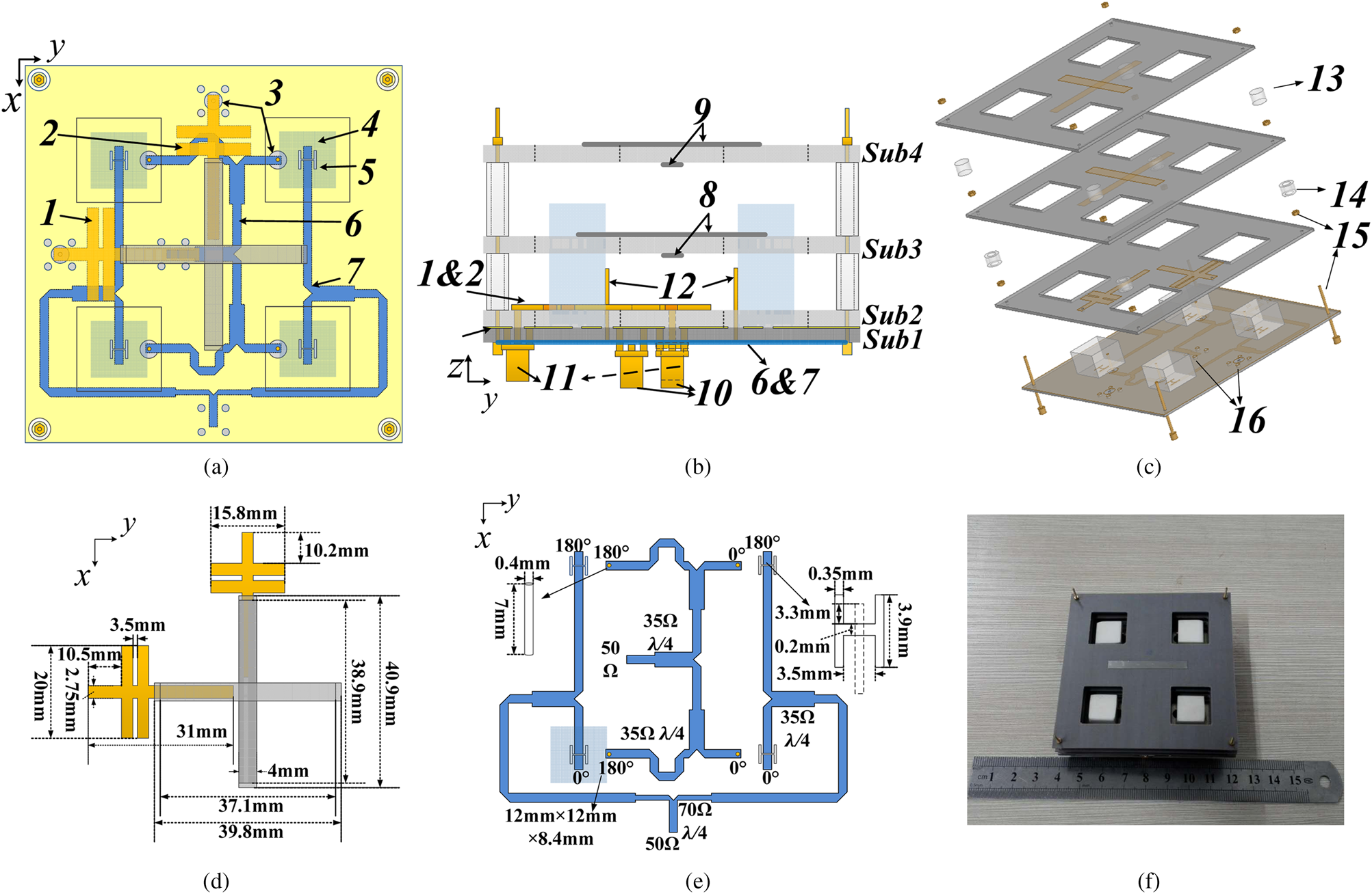
Fig. 1. Structure of proposed DBDP shared-aperture antenna. (a) Top view. (b) Side view. (c) Exploded view. (d) S band antennas and feed lines. (e) C band array and feed network. (f) Photo of proposed antenna.
Table 1. Comments for the structure of DBDP shared-aperture antenna subarray

Table 2. Details of substrates

Proximity coupled, stacked microstrip dipole is selected as the radiating element for S band, and the use of dipoles instead of slots can avoid the backward radiation and bring more convenience for broadening the bandwidth. The dimension of the printed dipoles can be approximately calculated, where l dipole is the length of the printed dipole, c is the speed of light in free space, ɛ eff is the effective dielectric constant, and f 0 is the center frequency of the S-band operation, which is 2.85 GHz in this design:
 $$l_{dipole}\approx \displaystyle{c \over {2f_0\sqrt {\varepsilon _{eff}}}} $$
F4BM220 (ɛ r = 2.2) is selected as the substrate of S band for broadening the bandwidth. Double tuning stubs are used in feed lines to provide more freedom for impedance matching and broaden the bandwidth. The feed lines are printed at the upside of sub2, the driven dipoles are printed at sub3, and the parasitic dipoles are printed at sub4. The driven dipoles and parasitic dipoles each excite one resonance point, and we can broaden the bandwidth by connecting the two resonance points, and by introducing two air layers under Sub3 and Sub4, the Q factor of dipoles are decreased, which further broaden the bandwidth. The two sets of stacked microstrip dipoles are crossed in the center at the positive and negative sides of two substrates respectively for dual-polarized, as Fig. 1 shows.
Several variables can be used to adjust the S band antenna such as the spacing between Sub2 and Sub3 (h 1), Sub3 and Sub4 (h 2), the spacing between two tuning stubs, the position of tuning stubs, the length of tuning stubs, and the length of dipoles/parasitic dipoles. The h 1 and h 2 are very crucial variables in that they can affect both polarization ports, but other variables affect only one port. Moreover, h 1 is more important, because when the spacing between Sub2 and Sub3 changes, the spacing between Sub2 and Sub4 changes too. So adjusting spacing values, especially h 1, has the highest priority. Figure 2 shows the simulated reflection coefficient of S-band dipoles with different values of h 1 and h 2, the change of h 1 has a significant influence on the reflection coefficient of both ports, and both ports achieve best reflection coefficient values when h 1 = 3.5 mm. Comparatively, the reflection coefficient of two ports is not so sensitive to h 2, when h 2 is increased from 3 to 6 mm. The worst reflection coefficient value decreased from −10.5 to −18.7 dB for H-port, and from −9.9 to −18.5 dB for V-port, however, when h 2 is increased, the two resonance points of both ports would be closer, which leads to a bandwidth loss. Therefore, 4 mm is selected as the value for h 2 after trade-off between reflection coefficient and bandwidth. Then we can use the optimized spacing values to adjust other variables for further optimization, and other optimized parameters are shown in Fig. 1(d).

Fig. 2. Simulated reflection coefficient of S-band dipoles with different values of h 1 and h 2. (a) Reflection coefficient with different values of h 1 for H-port (h 2 = 4). (b) Reflection coefficient with different values of h 1 for V-port (h 2 = 4). (c) Reflection coefficient with different values of h 2 for H-port (h 1 = 3.5). (d) Reflection coefficient with different values of h 2 for V-port (h 1 = 3.5).
Dual-polarized DRAs (Al2O3, ɛ r = 9.8) working in the fundamental mode are employed as radiating elements for the C band. The resonant frequency of rectangular DRA is determined by its dimensions, materials, and working mode, and can be calculated by the equations given in [Reference Mongia and Ittipiboon25].
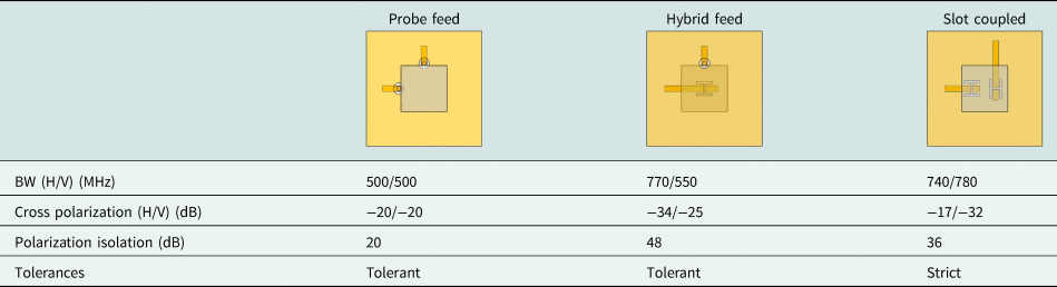
In this shared aperture antenna, the feedlines of C band DRAs are reserved under the ground, so three feeding schemes (probe fed, aperture coupled, and hybrid fed) are selected as candidates. The simulated results are shown in Table 3. Although the bandwidth of hybrid feed DRA is narrower than the slot-coupled DRA, the hybrid feed DRA owns better polarization isolation, lower cross-polarization and has more tolerant of fabrication errors, so that the hybrid feed DRA is selected for radiation element of C band.
Table 3. Comparison of three feeding schemes
DRAs with low dielectric constant material provide desired bandwidth, the “pair-wise” anti-phase feed technique is used to reduce the cross-polarization of array. F4BM265 (ɛ r = 2.65) is selected as the substrate of C band in order to make the feed line thinner for setting power dividers of two polarizations. In order to set the 2 × 2 DRAs, we need four perforations in Sub2, Sub3, and Sub4 respectively. Feed networks for DRA array are necessary in order to improve integration, and two 4-way 0°/180° differential power dividers for each polarization are designed and printed on the backside of sub1, separated from the feed lines of S band by ground, and in this way, the isolation between bands is improved largely. The structure of C band DRA array is shown in Fig. 1, and some key parameters are given in Fig. 1(e).
Results and discussion
The proposed antenna is designed and simulated by using Ansoft HFSS15, and the prototype antenna is manufactured and tested to validate the design as shown in Fig. 3. The simulated and measured S-parameters and radiation patterns for the S band are shown in Figs 4 and 5. A measured bandwidth from 2.72 to 2.99 GHz is achieved for both polarizations, i.e., 9.5%. A good bandwidth of S band is obtained, but a little narrower than simulated, since an uncontrollable spacing would exist between Sub1 and Sub2 due to the solder joint, besides, the length of the hard plastic tube may also produce a little deviation. The isolation is over 25 dB between the two orthogonal ports in the operating band, the co-polarization radiation pattern is symmetrical, and cross-polarization levels are better than −20 dB in both planes, which shows good agreement between simulated and measured results.

Fig. 3. Experimental setup.

Fig. 4. Measured and simulated S-parameter of S band port and C band port.
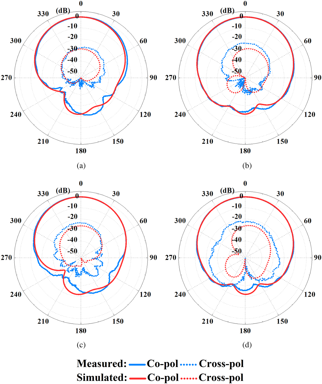
Fig. 5. Measured and simulated radiation patterns at S band. (a) H-pol E plane. (b) H-pol H plane. (c) V-pol E plane. (d) V-pol H plane.
The simulated and measured S-parameters for the C band are shown in Fig. 4. The antenna has an impedance bandwidth from 5.25 to 5.7 GHz for both orthogonal ports. The obtained bandwidth is 450 MHz, and there is a 50 MHz frequency shift in the resonance points between simulated and measured results since the dielectric constant and the size of DRAs is not precise enough. The measured isolation between polarizations is better than 35 dB, 5 dB lower than simulated data, and this may be caused by the influence of manufacturing and assembly error. The radiation patterns of C band are shown in Fig. 6, the co-polarization radiation pattern of the C band is symmetrical and accord with simulated. However, the cross-polarization level within the main lobe is less than −25 dB, which is worse than simulated, because the position errors of the DRA array would occur inevitably and the symmetrical characteristic of the array is affected when fixing DRAs on the ground by glue manually.
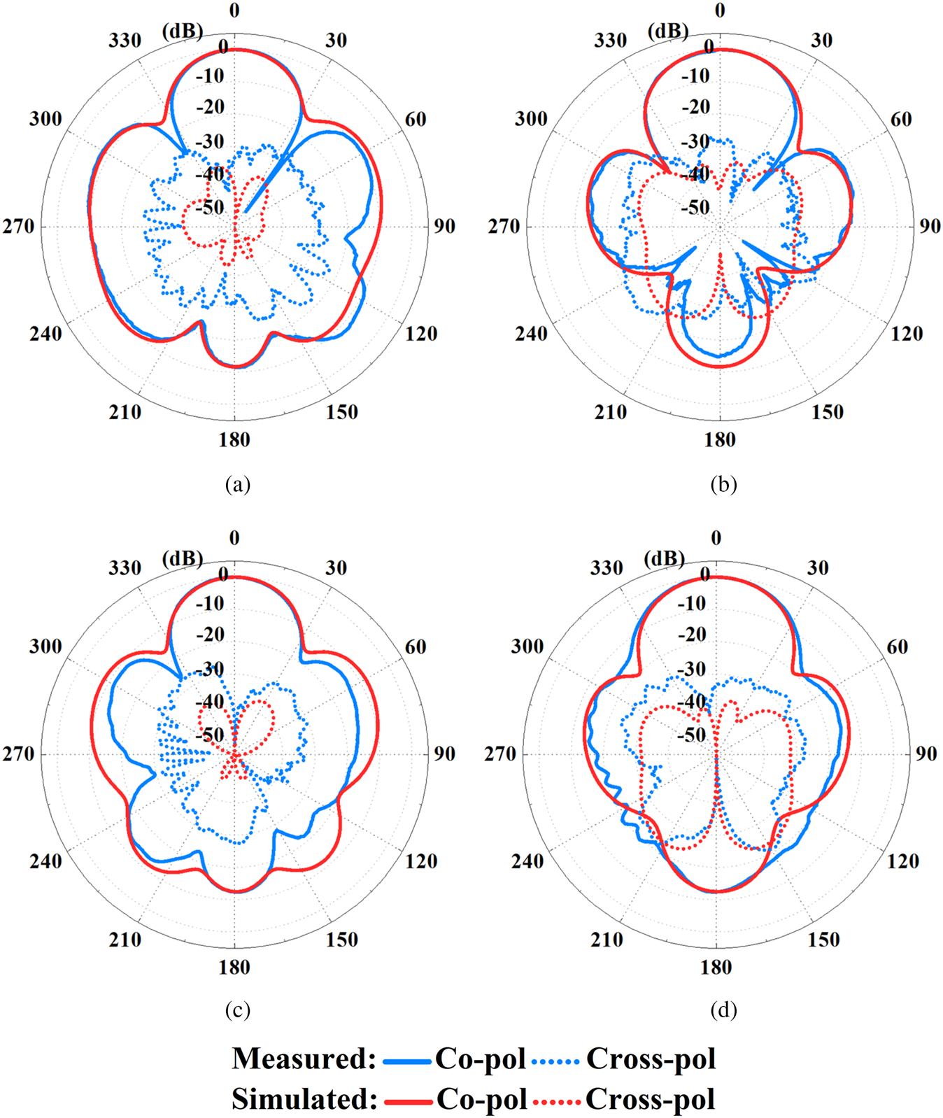
Fig. 6. Measured and simulated radiation patterns at C band. (a) H-pol E plane. (b) H-pol H plane. (c) V-pol E plane. (d) V-pol H plane.
Since elements of two bands are set in the same aperture, so the mutual coupling is worthy of being studied, the simulated distribution of the vector E field is shown in Fig. 7. At 2.85 GHz, when only S band is excited, there is a strong E field distribution on S band feed lines, driven dipoles, and parasitic dipoles, and a weaker E field distribution on C band feeding probe, however, there is no E field distribution in DRAs because the frequency is far lower than the frequency of fundamental mode and the DRAs would not be excited, and benefited from the non-metal structure of DRAs, the parasitic capacitance between DRAs and dipoles would not be produced and E filed would hardly be coupled into DRAs. Furthermore, there is almost no E field distribution on the feed network of C band benefited from the separation by ground. At 5.5 GHz, when only C band is excited, the strong E field is distributed in DRAs and feed networks of C band. In contrast, there is almost no E field distribution on antennas and feed lines of S band. When a single band is excited, the weaker E field distributes on the antenna of another band, the better isolation shared aperture antenna has, which indicate the good isolation between two bands. Besides, the simulated and measured isolation results are also shown in Fig. 8, and we can see the worst-case measured isolation between bands is 35 dB, which reveals that good isolation and little mutual interference are obtained.
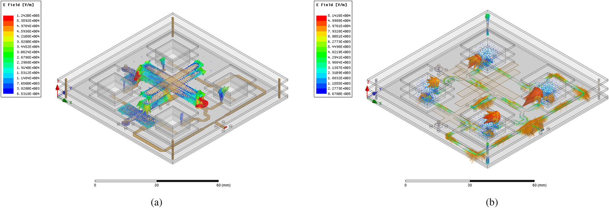
Fig. 7. Vector E field of proposed antenna. (a) At 2.85 GHz, when only S band is excited. (b) At 5.5 GHZ, when only C band is excited.

Fig. 8. Simulated/measured band isolation.
Some main performances of several small FR shared-aperture antennas are compared in Table 4. The comparison results show that the proposed antenna has good comprehensive performance and the main advantage of the proposed shared-aperture antenna is high isolation.
Table 4. Comparison between the proposed antenna and previous models

Conclusions
In this paper, a novel DBDP shared-aperture antenna with a FR of about 1:2 is presented. Several techniques are used to broaden the bandwidth, improve the polarization isolation, and reduce the cross-polarization level. Furthermore, high isolation between bands and low mutual interference are achieved benefited from the use of DRA. The prototype antenna is fabricated and measured. The measured results show that the antenna covers the frequency bands of 2.72–2.99 GHz and 5.25–5.7 GHz with S 11 below −10 dB, the isolation between polarizations is better than 25 dB for S band and 35 dB for C band, the cross-polarization level for S and C bands is lower than −20 and −25 dB in the main lobe respectively, and the isolation between the two ports is over 35 dB. The proposed antenna has many advantages such as low cost, high integration, and low mutual interference. In addition, the proposed antenna has geometrical symmetry, which shows it has the potential of expanding into a large aperture.
 JiaChen Xu was born in Shannxi Province, China, in 1991. He received his B.Sc. degree and M.Sc. degree from the School of Electrical and Information, Northwestern Polytechnical University in Xi'an city, China, in 2013 and 2016, respectively. He is presently working on his doctoral degree at the School of Electronics and Information, Northwestern Polytechnical University in Xi'an city, China. His research interests include dielectric resonator antennas and shared aperture arrays.
 BoZhang Lan was born in Shannxi Province, China, in 1992. He received his B.S. degree in electronic science and technology from the HeFei University of Technology in HeFei city, China in 2014, and received his M.S. degree in electromagnetic filed and microwave technology from Northwestern Polytechnical University in Xi'an city, China in 2016. He is working toward his Ph.D. degree at Northwestern Polytechnical University. His research interests include reconfigurable antennas and microwave filters.
 JiaKai Zhang was born in Shannxi Province, China, in 1990. He received his M.Sc. and B.Sc. degrees from the School of Electronics and Information, Northwestern Polytechnical University in Xi'an city, China, in 2012 and 2015, respectively. He is presently working on his doctoral degree at the School of Electronics and Information, Northwestern Polytechnical University in Xi'an city, China. His research interests include electromagnetic metamaterials and antenna RCS reduction.
 ChenJiang Guo was born in Shannxi Province, China, in 1963. He is CIE Senior Member, Antenna Society Committee Member. He received his M.Sc., B.Sc., and Ph.D. from the School of Electronics and Information, Northwestern Polytechnical University in Xi'an city, China, in 1984, 1987, and 2007, respectively. He is a professor in the School of Electronics and Information, NWPU. He has published more than 140 research papers. His research interests include EMI/EMC, antenna theory and design, and microwave circuit design.
 Jun Ding was born in Shannxi Province, China, in 1964. She received her M.Sc., B.Sc., and Ph.D. from the School of Electronics and Information, Northwestern Polytechnical University in Xi'an city, China, in 1986, 1989, and 2005, respectively. She is a professor at the School of Electronics and Information, NWPU. She has published more than 100 research papers. Her research interests include electromagnetic metamaterials, antenna theory and design, and microwave circuit design.


