


I. INTRODUCTION
The use of radio frequency identification (RFID) systems has become widespread in a variety of applications. Most of RFID systems operate in the megahertz frequency range. Generally speaking, the higher the frequency band, the longer is the reading range. Recently, 2.45 GHz band RFID systems are under active development, since they are able to provide better features such as higher reading speed and longer reading range than other RFID systems operating within a different frequency band. A RFID reader is a radio transceiver: a transmitter and receiver that works together to communicate with the tag. The RFID readers can be classified into handheld readers and fixed readers according to their mobility.
Handheld RFID readers reported are all single port with various structures [Reference Hsu and Huang1–Reference Mohammad and Nasser6]. RFID system consists of a tag and reader. The reader transmits a continuous wave (CW) signal to a tag and the tag backscatters modulated signal to the reader. In the receiving part of reader, the backscattering signal is directly coupled with the strong transmitting CW signal, which degrades the receiving sensitivity of reader. The directly coupled CW signal is much larger than the backscatter signal from the tag and the receiving part of the reader should detect the weak signal closed to such a strong in-band interfere. The leakage from the transmitting part to the receiving part can be an important limit in the receiving sensitivity. Therefore, it is essential to separate transmitting and receiving parts with dual ports to achieve high isolation between them.
Fixed RFID reader antennas in 2.4 GHz band have been studied more extensive than handheld ones [Reference Chou, Hung, Wang, Chou, Tung and Nepa7–Reference Zhang, Chen, Jiao and Zhang17]. Microstrip patch antennas [Reference Chou, Hung, Wang, Chou, Tung and Nepa7–Reference Mobashsher, Islam and Misran8] and microstrip antennas [Reference Buffi, Serra, Chou and Manara9–Reference Grilo, Arnold, Goncalves, Bravo-Roger, Moretti and Lima14] with single port are proposed for RFID reader applications. As handheld RFID reader antennas, fixed ones utilize single port to transmit and receive signal but also have sensitivity problem. To realize a reader antenna with separate transmitting and receiving ports is not an easy task. Research papers for this goal are rare, although there have been some partial efforts [Reference Jung and Lee15–Reference Zhang, Chen, Jiao and Zhang17]. However, antennas with dual ports have received considerable attention in 915 MHz band. Among dual ports antennas in both 2.4 GHz band and 915 MHz band, aperture-coupled microstrip patch antennas are the most suitable candidates. In [Reference Jung and Lee15–Reference Zhang, Chen, Jiao and Zhang17] antennas use aperture-coupled patch structure, but they perform poor isolation between the orthogonal feeding ports due to high mutual coupling. It is desirable to have isolation of lower than 25 dB between the transmitting and receiving ports in order to have the smooth transmission and less cross-talk in the circuits. A dual ports antenna applying aperture-coupled patch structure is designed in this paper. The measured −25 dB isolation band from 2.3 to 2.55 GHz covers the 2.4–2.48 GHz. The whole volume of the designed antenna is 80 mm × 80 mm × 6.8 mm, which is comparable smaller than the reported ones [Reference Jung and Lee15–Reference Zhang, Chen, Jiao and Zhang17]. Table 1 compares the reported dual ports RFID reader antennas in terms of return loss bandwidth, isolation bandwidth, and antenna volume. Since, the antenna is to be used within a handheld RFID reader, the size of the antenna in general should be around 100 mm length and width, and around 10 mm in thickness [Reference Nikitin and Rao18]. Therefore, open literatures [Reference Jung and Lee15, Reference Padhi, Karmakar and Law16] described reader antennas with dual ports are comparable large to be mounted into a handheld RFID reader, however they are suitable for fixed readers.
Table 1. Comparison of the proposed dual ports antenna with reported ones.

In this paper, a novel design of an aperture-coupled patch antenna with separate receive (Rx) and transmit (Tx) ports of high isolation is introduced for RFID ISM band (2.4–2.48 GHz) applications. E-shaped slots in the ground plane and modified T-shaped feeding lines are used to achieve high isolation and the compactness. The rest of the sections are organized as follows: Section II presents the detail design and principle of the aperture-coupled patch antenna. The measured ports isolation and impedance matching of the proposed antenna are discussed in Section III. The effects of variation in position of stub and length of slot on isolation and impedance matching are analyzed in Section IV. The conclusions are given in Section V.
II. ANTENNA STRUCTURE AND DESIGN
Among dual-polarized antenna designs, aperture-coupled microstrip patch antennas are the most suitable candidates for RFID application. Aperture-coupled feeding is preferred to other feeding mechanisms of microstrip patch antenna due to its greater design flexibility, easy fabrication, and low cost. Several dual-polarized antennas have approximately −20 dB isolation between Rx and Tx ports, thus the backscattering signal at Rx port is strongly coupled to the Tx port, which decreases reader sensitivity. In traditional designs of aperture-coupled antenna, they are using two off-center orthogonal apertures or two crossed-apertures located at the center of patch. But these techniques require high air layer in order to reduce the coupling between two feeding lines, antennas are inconvenient of integrating in RFID reader due to its increasing volume. Consequently E-slot is introduced to couple the energy of the T-shaped feeding lines to the square patch for increasing isolation between Rx and Tx ports and decreasing the volume.
The configuration of the aperture-coupled antenna is shown in Fig. 1(c), the unit is mm. It consists of two FR4 substrates with dielectric constant of 4.4 and loss tangent of 0.02. A single-layer substrate (56 mm × 56 mm × 1.2 mm) is suspended 4 mm above the double-layer substrate (80 mm × 80 mm × 1.6 mm). A square patch of 50 mm × 50 mm is etched on the top side of the single-layer substrate. Two 50 Ω modified T-shaped microstrip lines with width of W f = 3 mm and length of L s = 43 mm are fed by separate ports 1 and 2 on the bottom side of the double-layer substrate. The mathematical equations for calculating the W f and L s are as follows:
 $$\displaystyle{{{W_f}} \over h} = {\left( {\displaystyle{1 \over 8}{e^A} - \displaystyle{1 \over {4{e^A}}}} \right)^{ - 1}},$$
 $$A = \displaystyle{{{Z_c}\sqrt {2({\varepsilon _r} + 1)}} \over {119.9}} + \displaystyle{1 \over 2}\displaystyle{{{\varepsilon _r} - 1} \over {{\varepsilon _r} + 1}}\left( {\ln \displaystyle{\pi \over 2} + \displaystyle{1 \over {{\varepsilon _r}}}\ln \displaystyle{4 \over \pi}} \right),$$
 $${L_s} \approx \displaystyle{{{\lambda _g}} \over 4},$$
 $${\lambda _g} = \displaystyle{{{\lambda _0}} \over {\sqrt {{\varepsilon _r}}}}, $$
where Z c is the characteristic impedance of the feeding line, λ g is the dielectric wavelength, λ 0 is the air wavelength, ε r is the effective dielectric constant and h is the substrate thickness. The substrate thickness, h, in this design is 1.6 mm. The ground plane is printed on top side of the substrate and two E-slots are etched on it. The slots change the current path on the ground and generate high isolation. The proposed antenna uses a square microstrip patch antenna as a radiator and E-shape apertures in the ground plane of the antenna to couple microwave energy from the feeding lines. In most aperture-coupled patch antennas, the feeding lines substrate enables the use of a thin, high-dielectric constant substrate. The radiator is printed on a thick, low-dielectric constant substrate, which is desirable for getting a large bandwidth and good radiation efficiency. However, the two substrates in this design are both FR4, with different thickness. In addition, spurious radiation from the feeding lines is eliminated due to ground plane shielding, which results in a very low cross-polarization level.

Fig. 1. (a) Top view of antenna-1, (b) top view of antenna-2, (c) configurations of antenna-3, and (d) prototype of the antenna-3.
In Fig. 1 two initial designs of the proposed antenna are presented. The antenna design is started from an antenna fed by modified T-shape feeding line with U-slot (antenna-1). An improvement is achieved by inserting a rectangular slot to U-slot to obtain wideband isolation (antenna-2). By properly adding one more stub to modified T-shaped feeding line, the antenna realizes good impedance matching (antenna-3).
U-slots are modified in the ground plane and stubs are added in the end of the feeding lines for improving isolation and impedance matching. The ports isolation, return loss, and peak gain of antenna-1, antenna-2, and antenna-3 are shown in Fig. 2, respectively. It is clearly seen that introducing a slot to antenna-1 enlarges the ports isolation bandwidth in Fig. 2(a) and adding a stub to antenna-2 enhances the impedance matching dramatically in Fig. 2(b). Figure 2 (c) indicates that introducing a slot overturns the increasing trend of peak gain of antenna-1 and adding a stub increases the peak gain of antenna-2 in low band.

Fig. 2. Characters of three antennas: (a) ports isolation, (b) return loss, and (c) peak gain.
To investigate the mechanism of mutual coupling between two ports, current distributions in different layers under the patch have been simulated with port 1 excited and port 2 terminated with 50 Ω. The current distribution at 2.45 GHz on the ground plane, feeding line and patch of antenna-1, antenna-2, and antenna-3 are illustrated in Figs 3–5, respectively.

Fig. 3. Current distribution on ground plane: (a) antenna-1, (b) antenna-2, and (c) antenna-3.

Fig. 4. Current distribution on feeding line: (a) antenna-1, (b) antenna-2, and (c) antenna-3.

Fig. 5. Current distribution on patch: (a) antenna-1, (b) antenna-2, and (c) antenna-3.
As shown in Fig. 3(a), the current concentrates in the left arm of the lower U-slot and it couples with the upper U-slot. The ports isolation increases much since the electromagnetic energy of port 1 is highly coupled to port 2. For decreasing ports isolation, a slot is added in the middle of U-slot and the ports isolation is improved effectively as shown in Fig. 3(b). The current at the end of upper U-slot becomes weaker and the current at the left arm of the lower U-slot flows to the right arm. As a result, the electromagnetic energy of port 1 is coupled less with port 2. It can be seen in Fig. 3(c) that surface current is flowing along the feeding line from ports 1 to 2 and gradually attenuated. The current around port 2 is greatly weaker than that around port 1. It has demonstrated an excellent isolation between ports 1 and 2.
The current concentrates in the end of feeding line 1 describing in Fig. 4(b), and it is much stronger than rest part of the feeding line 1. It results in bad impedance matching shown in Fig. 2(b). In this paper, stub 2 is introduced around stub1 to increase the capacitive between two stubs, thus reduces the inductive of stub 1. The impedance matching is improved dramatically presenting in Fig. 2(b).
We can see that current on patch of antenna-3 distributes the most strongest in Fig. 5(c). Hence, the antenna-3 has the biggest peak gain.
The simulated surface current distributions on the radiating patch at 2.45 GHz are shown in Fig. 6 for different time frames: t = 0 (0°), T/4(90°), T/2(180°), 3 T/4(270°). It is displayed that surface currents cause linear polarization with time. Since the proposed antenna has a symmetrical structure, the Tx and Rx ports can interchange to create linear polarization. Thus, the proposed antenna has dual linear polarization in one antenna structure and orthogonal polarization improves isolation between two ports.
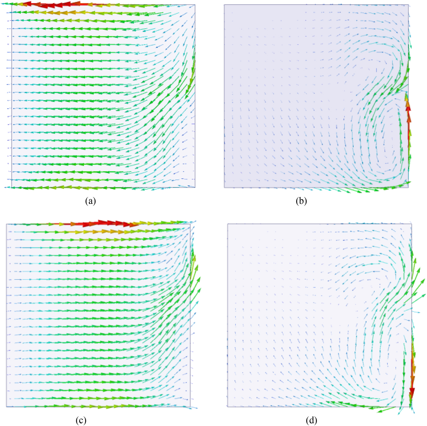
Fig. 6. Radiating patch surface current distributions for four different phase intervals. (a) 0°, (b) 90°, (c) 180°, and (d) 270°.
III. PERFORMANCE OF APERTURE COUPLED ANTENNA
Figs 7(a)–7(c) illustrate the simulated and measured ports isolation, return loss, and peak gain of the antenna, respectively. The measured return loss is less than −10 dB over the frequency band of 2.32–2.6 GHz. The measured −25 dB bandwidth of 2.3–2.55 GHz is obtained with average −35 dB. The antenna exhibits the measured peak gain from 3 to 1.6 dBi according to the frequency band of 2.4–2.48 GHz. In microwave band, antenna gain is not critical since active tags are commonly used in many applications. The measured and simulated return loss, isolation, and peak gain show good agreement.

Fig. 7. The characters of proposed antenna: (a) ports isolation, (b) return loss, and (c) peak gain.
Fig. 8 shows the measured radiation patterns at 2.45 GHz with port 1 excited in the orthogonal XOZ- (phi = 0°) and YOZ (phi = 90°)-planes with angular step of 10°. Due to the symmetrical characteristic of antenna, there is only a slight difference of radiation patterns between two ports and Fig. 8 just show the results of port 1. The main beam of radiation is fixed in the broadside direction. The radiation pattern in the XOZ-plane is omnidirectional, but that in the YOZ-plane is unidirectional.

Fig. 8. Measured radiation patterns of proposed antenna at 2.45 GHz.
IV. PARAMETERS SIMULATION AND ANALYSIS
To further examine the appropriate ports isolation and impedance-matching condition caused from the slots and the stubs, HFSS, based on the finite element method, is used to numerically investigate and optimize the proposed antenna configuration. One physical attribute of the antenna is independently varied, while the other parameter is kept unchanged. For clear visualization, the final optimized parameters are depicted with red line in each simulation figure. The final optimized values are stub-x = −1 mm and slot-L = 45 mm.
A) The effect of the stub-x
The dependencies of the return loss and isolation on stub-x are described in Fig. 9. Figure 9(a) indicates that ports isolation has one variation trend with stub-x of 3 mm, while the other three parameter values of stub-x have the other trend. The ports isolation (<−25 dB) bandwidth is 250 MHz ranging from 2.3 to 2.55 GHz. Figure 9(b) illustrates that return loss is increasing with enlarging the distance of stub-x. It is concluded from the results that stub-x plays a significant part in tuning ports isolation and return loss.

Fig. 9. Antenna characters for different values of stub-x. (a) Ports isolation and (b) return loss.
B) The effect of slot-L
The effect of various dimensions of slot-L on ports isolation and return loss are shown in Fig. 10. It is clearly seen in Fig. 10(a) that slot-L of 45 mm has the largest bandwidth of 250 MHz and resonates at 2.33 GHz. However, slot-L of the other three parameter values has the same bandwidth of 200 MHz and resonates at 2.45 GHz. Figure 10(b) depicts that the return loss bandwidth with various parameters covers 2.3–2.6 GHz. The obtained results show that slot-L has a minor effect on the return loss.

Fig. 10. Antenna characters for different values of slot-L: (a)ports isolation and (b) return loss.
V. CONCLUSION
An E-shaped aperture-coupled patch antenna with dual ports is designed for handheld RFID readers to enhance sensitivity. It is low cost and easy to integrate in the RFID devices for its height of 6.8 mm. The proposed antenna presents impedance matching of around −16 dB and ports isolation of around −30 dB. The measured −10 dB impedance matching bandwidth and −25 dB ports isolation bandwidth range from 2.32 to 2.6 GHz and from 2.3 to 2.55 GHz, respectively.
ACKNOWLEDGEMENTS
The paper is supported by “the Fundamental Research Funds for the Central Universities” (No. JB141107) in China.
 Bo Wang received his B.S. degree from Xi'an University of Technology of Xi'an, Shaanxi, China, in 2008. He received his M.S. degree from Xidian University, Xi'an, Shaanxi, China, in 2011. He is presently pursuing the Ph.D. degree in Microelectronics and Solid States Electronics at Xidian University. During his M.S. program, he designed and tested several amplifiers including low noise, high gain and high linear amplifiers. His present research interest is RFID reader and tag antenna design and measurement.
 Yiqi Zhuang is presently a Professor and the President of Institute of Microelectronics, Xidian University, Xi'an, China. His research interests include communication and power system integration, noise and reliability of Microelectronic device application technology, and high-performance RFIC design.
 Xiaoming Li received his Ph.D. degree in Microelectronics and Solid States Electronics from Xidian University, Xi'an, China, in 2008. He is presently an Associate Professor of Institute of Microelectronics at the same university. His research interests include SoC design methodologies, NVM and RF integrated circuit design.
 Weifeng Liu received his B.E. and M.E. degrees in Microelectronics from Xidian University, Xi'an, China, in 2002 and 2005, respectively. His research interests include SoC design methodologies in Nanometer CMOS technology, digital and mixed-signal VLSI, ultra-low-power integrated circuits and systems, digital-integrated circuits.


