


I. INTRODUCTION
With the fast development of the mobile communication system, multiple systems such as 3G, 4G, wireless local area network (WLAN), worldwide interoperability for microwave access (WiMAX), and long term evolution (LTE) will coexist in the future. Consequently, the number of the base station antenna is increasing immensely and the structure of base station antenna becomes more and more complicated. In addition, the increasing demands for base station antennas are put forward, including wideband, good unidirectional radiation patterns, stable gain, low cross-polarization, miniaturization, low cost, and so on. In order to meet these demands, a new magneto-electric (ME) dipole antenna was designed by Luk and Wong in 2006 [Reference Luk and Wong1]. Over the operating frequency band, this type of antenna has not only a broad bandwidth, stable gain, low cross-polarization, and wide half-power beamwidth, but also the identical radiation patterns in E- and H-planes.
Due to the notable advantages of the ME dipole antenna, many researchers have made further researches and many novel ME dipole antennas with good electrical characteristics were proposed [Reference Wu and Luk2–Reference Ta and Park8]. In [Reference Wu and Luk2], the designed antenna obtains wideband and dual-polarized characteristics. In [Reference Liang, Jiao, Li and Ni3], via introducing a wideband 90° Schiffman phase shifter, a circularly polarized ME dipole antenna is presented. In [Reference Ge and Luk4], a novel ultra wideband ME dipole antenna is proposed. In [Reference Ge and Luk5], a new band-reconfigurable antenna is designed by using ME dipole technology. However, almost all the ME dipole antennas have a bulky three-dimensional structure, especially the large reflector. This drawback makes the conventional ME dipole antennas uneasy to be installed. Furthermore, due to the restriction to space size of the array element, they are also unsuitable for beam steering in array application.
In order to reduce the space size of the ME dipole antenna, plenty of effective methods were proposed in recent literatures. In [Reference Ge and Luk9], the proposed antenna adopts the vertically oriented folded shorted patches to obtain a low-profile structure of 0.173λ in thickness. In [Reference Ding and Luk10], the antenna's thickness achieves 0.097λ by introducing an obtuse-triangular structure as a magnetic dipole. Paper of Idayachandran and Nakkeeran [Reference Idayachandran and Nakkeeran11] directly changes the square ground into minimum ground and this method reduces the height of the horizontal radiation patch. These above antennas have acquired a certain effect, but they still have a three-dimensional structure and cannot meet the restriction to space size (close to 0.5λ) for array elements. Therefore, Tang and Xue [Reference Tang and Xue12] proposed a novel vertical planar printed ME dipole antenna and its space size is reduced immensely. But this antenna only obtains an impedance bandwidth of 17.1% and it still has a large vertical ground plane. Furthermore, in [Reference Feng, Yin and Li13], the designed antenna is completely printed on the both sides of the substrate, and achieves a planar structure and quasi-omnidirectional radiation patterns. However, the radiation patterns of the proposed antenna in the H-plane are unstable over the operating frequency band.
In this paper, a new uniplanar wideband ME dipole antenna with stable unidirectional radiation patterns is proposed. The conventional bow–tie antenna with the tapered slot works as an electric dipole, and the semi-circular loop operates as a magnetic dipole. For obtaining good impedance matching, a microstrip-to-coplanar stripline transition balun is adopted. Additionally, two directors are utilized for higher and more stable gain. By introducing a small-size coplanar ground plane, the proposed antenna achieves a uniplanar structure, which is easily fabricated and manufactured at a low cost. Meanwhile, the uniplanar structure is suitable for the H-plane beam steering in array application.
II. ANTENNA DESIGN AND GEOMETRY
The geometry of the proposed antenna is shown in Fig. 1. The overall size of the proposed antenna is W × L. The designed antenna is printed on the single-layer Duroid 5880 dielectric substrate with the permittivity of 2.2 and thickness of 0.787 mm. The antenna consists of four portions, including a ME dipole, ground plane, a microstrip-to-coplanar stripline transition balun, and two directors. Figure 1(a) depicts the top layer of the proposed antenna. The conventional bow–tie radiation structure with the flare angle of θ is adopted as an electric dipole for wideband. The slot in the middle of the bow–tie patch is modified into a tapered structure for widening the bandwidth and improving the impedance matching. The minimum width of the tapered slot is finally chosen to be s = 4 mm. The semi-circular loop together with the ground between the loop works as a magnetic dipole. When an electric dipole and a magnetic dipole are excited simultaneously, a ME dipole comes into being. Compared with the traditional vertical ground plane, the modified coplanar ground reduces the space size of the proposed antenna immensely and achieves a uniplanar structure. This modification decreases the cost of the manufacture and fabrication and has a high application value for array design. Additionally, a microstrip-to-coplanar stripline transition balun supplies a broad impedance bandwidth for the proposed antenna. Two directors with different lengths are adopted to obtain higher and more stable gain, which are based on the idea of Quasi-Yagi antenna design. Figure 1(b) shows the bottom layer of the proposed antenna. We can see that Γ-shaped strip feeding structure is printed on the back of the substrate for coupling the electromagnetic energy to the tapered slot. At the same time, a sub-miniature-A connector is connected to Γ-shaped strip for transmitting the excitation signal. The input characteristic impedance is chosen to be 50 Ω.
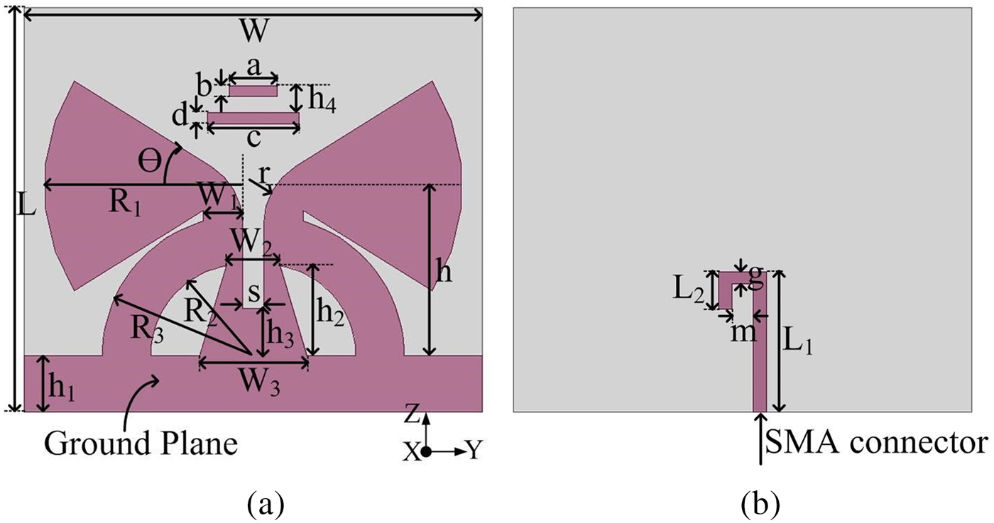
Fig. 1. Geometry of the proposed antenna: (a) top layer; (b) bottom layer.
All the dimensions of the proposed antenna in detail are depicted in Table 1.
Table 1. Dimensions of the proposed antenna.
λ is the free-space wavelength at the center frequency.
III. SIMULATION AND MEASUREMENT
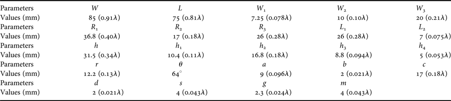
The prototype of the proposed antenna shown in Fig. 2 is fabricated and measured. The simulated results are obtained by using Ansoft HFSS. The antenna prototype is measured in an anechotic chamber.
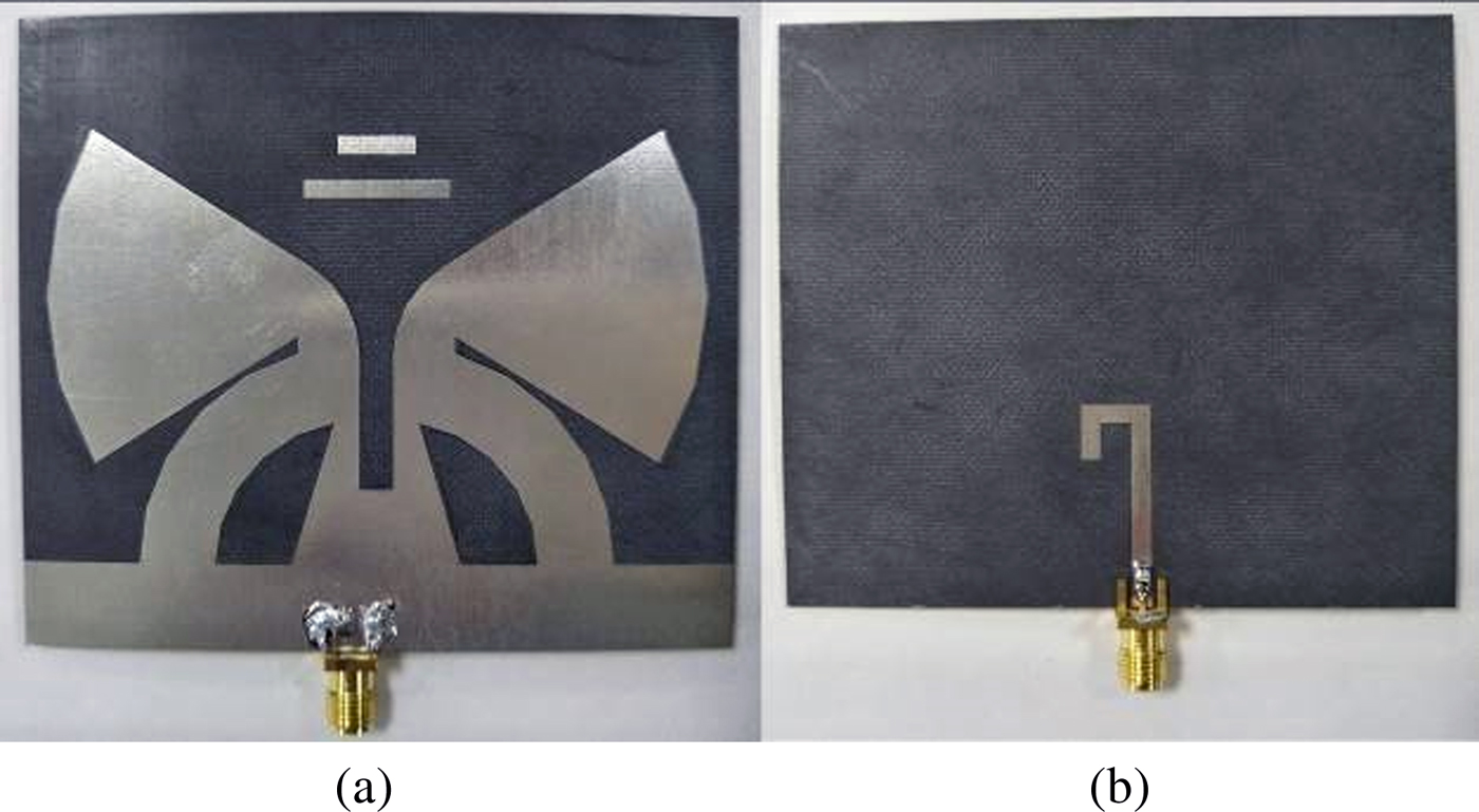
Fig. 2. Prototype of the proposed antenna: (a) top layer; (b) bottom layer.
Figure 3 presents the evolution process of the proposed antenna. The initial design named antenna I is shown in Fig. 3(a). By introducing a tapered slot, antenna II shown in Fig. 3(b) comes into being. Further, antenna III depicted in Fig. 3(c) adds on a director. Based on antenna III, the proposed antenna shown in Fig. 3(d) adds on the second director. Figure 4 illustrates the simulated voltage standing wave ratios (VSWR) and gains of the four antennas above. It is obvious that the simulated impedance bandwidth of the antenna II is from 2.30 to 4.16 GHz (VSWR ≤ 2), which is wider than the simulated bandwidth of antenna I from 2.20 to 3.85 GHz. Therefore, the tapered slot improves the initial antenna's impedance matching, especially in the high frequency. The proposed antenna achieves a wide bandwidth of 60.5% from 2.25 to 4.20 GHz (VSWR ≤ 2), which can cover WLAN (2.4–2.484 GHz), WiMAX (2.5–2.69/3.4–3.69 GHz), and LTE (2.5–2.69 GHz). Additionally, from Fig. 4, we can see that antenna II, antenna III, and the proposed antenna have the almost identical bandwidths, whereas the gains of three antennas are obviously different in the corresponding frequency bands. Antenna II obtains the simulated gain from 3.8 to 4.8 dBi. The gain of antenna III is 3.9–5.1 dBi. The proposed antenna finally achieves the gain of 5 ± 0.5 dBi over the operating frequency band. Via introducing two directors, the antenna gain is increased by 0.7 dBi and becomes more stable. In theory, the more the number of directors is, the more the gain of the antenna is increased. However, we finally choose two directors added on the antenna instead of three or more, mainly because by further simulation, it is found that when the third director is added on the antenna, the antenna gain is almost unchanged.
Fig. 3. Evolution process of the proposed antenna: (a) antenna I; (b) antenna II; (c) antenna III; (d) the proposed antenna.

Fig. 4. Simulated VSWRs and gains of the four antennas.
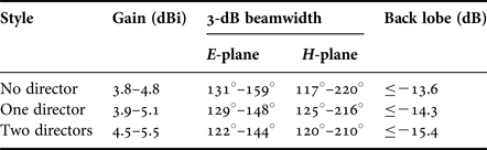
To investigate the effects of the number of the directors on the radiation patterns, the simulated parameters of the radiation patterns of the design antennas with the different number of directors are listed in Table 2. It can be seen that the number of the directors has a significant effect on the gain and 3-dB beamwidth of the radiation patterns of the designed antennas. As the number of the directors increases, the 3-dB beamwidth in the E-plane gradually decreases, whereas in the H-plane the 3-dB beamwidth is changed slightly. Therefore, by introducing the directors, the antenna directivity is enhanced. Ultimately, after comprehensive consideration, two directors are chosen to add on the proposed antenna. The simulated results show that over the operating frequency band, the 3-dB beamwidth in the E-plane ranges from 122° to 144°, while the 3-dB beamwidth in the H-plane ranges from 120° to 210°.
Table 2. Simulated parameters of the radiation patterns of the antennas with the different number of directors.
For explaining the principle of the proposed antenna further, the simulated surface current distribution at 2.8 GHz is shown in Fig. 5. The current distribution of the bow–tie patch presents a linear distribution and is similar to the half-wave dipole antenna. Hence, the bow–tie patch is equivalent to an electric dipole. Moreover, the current distribution of the semi-circular loop presents a ring-like current distribution; therefore, the semi-circular loop together with the ground between the loops works as a magnetic dipole. When the electric dipole and magnetic dipole are excited simultaneously, the complementary radiation patterns come into being.

Fig. 5. Simulated surface current distribution at 2.8 GHz.
In order to investigate the array composed of the proposed antenna elements, we use HFSS to simulate the four-element array. The geometry of the linear array for the H-plane beam steering is shown in Fig. 6. From the picture, we can see that the array has four ports. For obtaining the low side lobe and low mutual coupling between the elements, the distance between the elements is chosen to be G = 50 mm. At the same time, the G of 50 mm maintains the acceptable impedance matching within the whole operating frequency band. Figure 7 shows the mutual coupling between four ports. Over the operating frequency band, all the mutual couplings between elements are below −20 dB. Figure 8 depicts the simulated radiation patterns at 2.6, 3.3, and 4.0 GHz. It is seen that the radiation patterns of the E-plane keep stable, whereas the radiation patterns of the H-plane obtains a narrow beamwidth. Furthermore, the side lobe level of the H-pane increases with the frequency. But the side lobe level of the H-plane is less than −12 dB. The cross-polarization level is below −23 dB and the back lobe level is less than −15 dB. In the entire operating frequency band, the simulated gain of four-element array varies from 10.5 to 12.5 dBi. To further validate the array performance of the proposed antenna, the eight-element array is investigated under the circumstance of keeping the same value of the distance between elements, G = 50 mm. The simulated radiation patterns of the eight-element array at 2.6, 3.3, and 4.0 GHz are shown in Fig. 9. It can be seen that the antenna directivity in the H-plane is further enhanced. Furthermore, the cross polarization level is less than −22 dB, and the back lobe level is below −14 dB. Meanwhile, the side lobe level of the H-plane is less than −13 dB. Ultimately, the simulated gain of the eight-element array ranges from 14.6 to 18.5 dBi over the operating frequency band. Hence, it is demonstrated that the proposed antenna element is suitable for the H-plane beam steering in array application.
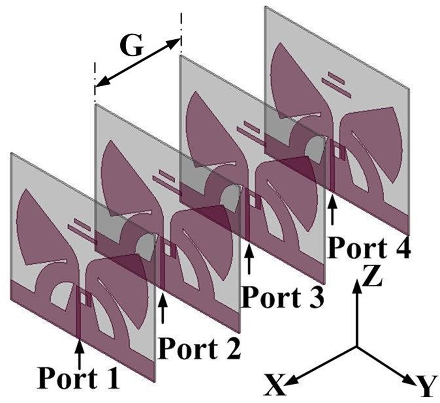
Fig. 6. Geometry of the linear array.
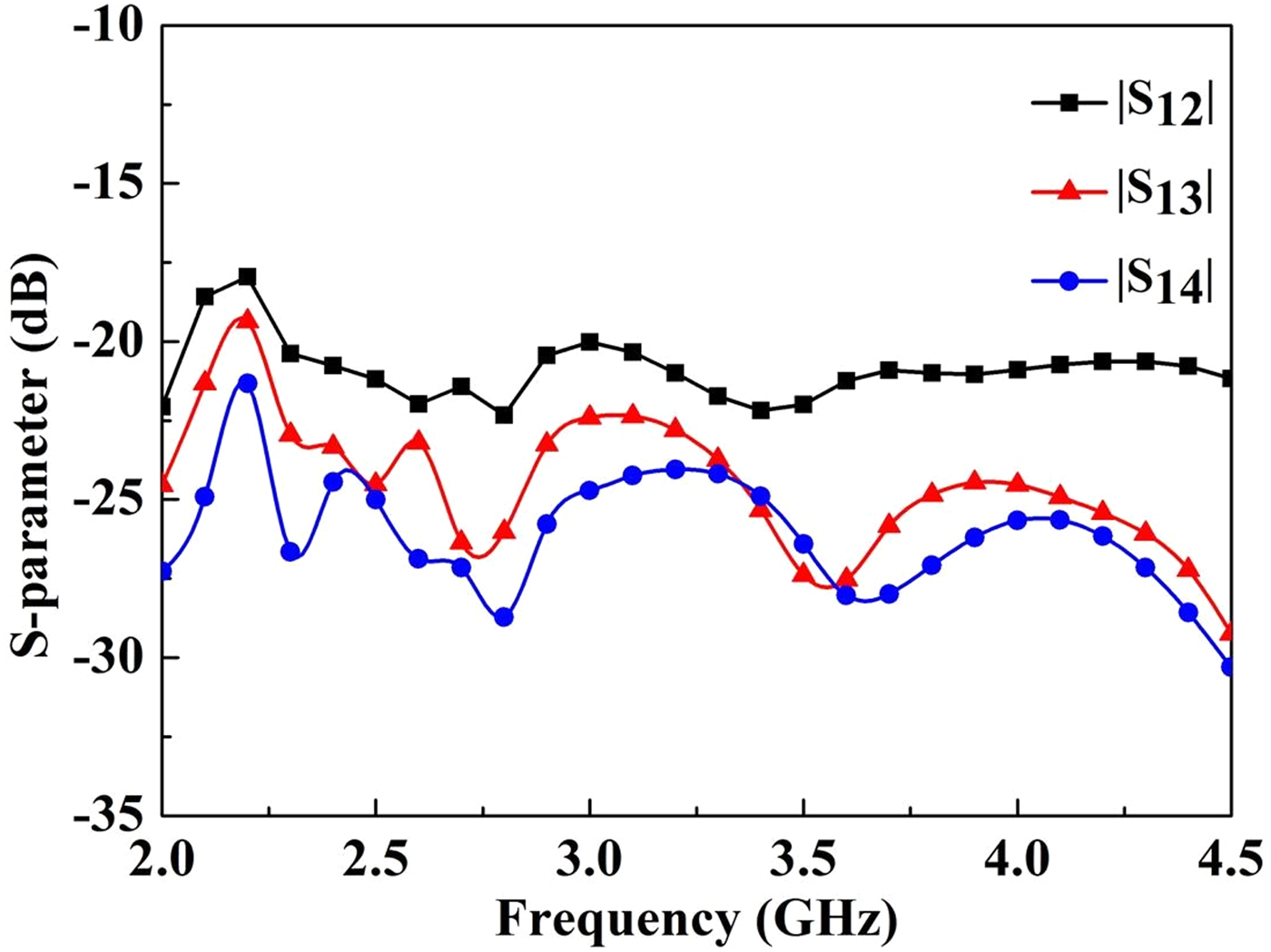
Fig. 7. Mutual coupling between the four ports.

Fig. 8. Simulated radiation patterns of four-element array at 2.6, 3.3, and 4.0 GHz.

Fig. 9. Simulated radiation patterns of eight-element array at 2.6, 3.3, and 4.0 GHz.
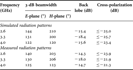
The simulated and measured VSWRs and gains of the proposed antenna are presented in Fig. 10. The measured results keep in good accordance with the simulated ones. As we can see, the measured bandwidth is 60.6% from 2.22 to 4.15 GHz (VSWR ≤ 2). The measured gain is stable and varies from 4.4 to 5.2 dBi, which is more than sufficient to cover the region of interest. Figure 11 illustrates the simulated and measured radiation patterns of the designed antenna at 2.6, 3.3, and 4.0 GHz. It is obvious that over the operating frequency band, the antenna obtains stable unidirectional radiation patterns with wide half-power beamwidth, low cross-polarization, and low back lobe. The measured cross-polarization level is less than −21.3 dB, and the measured back lobe level is below −14.3 dB. Moreover, by measurement, the proposed antenna achieves the broad 3-dB beamwidths in the E-plane (125°–140°) and in the H-plane (123°–206°) within the impedance bandwidth. Over the operating frequency band, the simulation agrees well with the measurement. The detailed parameters of simulated and measured radiation patterns of the proposed antenna are listed in Table 3.
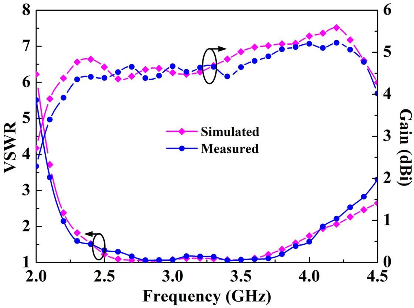
Fig. 10. Simulated and measured VSWRs and gains of the proposed antenna.
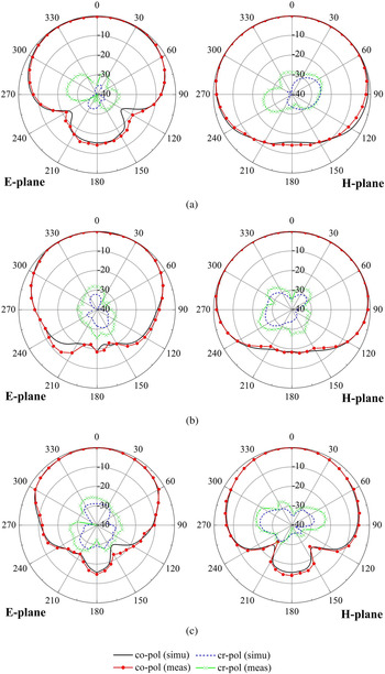
Fig. 11. Simulated and measured radiation patterns of the proposed antenna at: (a) 2.6 GHz; (b) 3.3 GHz; (c) 4.0 GHz.
Table 3. Detailed parameters of the simulated and measured radiation patterns.
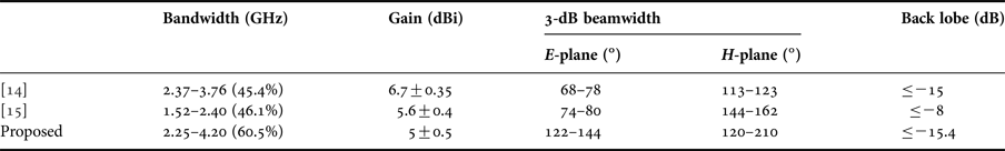
To my knowledge, there are many previous works investigating on the 3-dB beamwidth of the ME dipole antenna. Hence, for validating the performance of the proposed antenna further, the experimental results are compared with the previous literatures [Reference Li and Luk14, Reference Ge and Luk15] in Table 4. From the table, it can be seen that the proposed antenna obtains a broader impedance bandwidth from 2.25 to 4.20 GHz (60.5%) with VSWR <2. Meanwhile, the wider 3-dB beamwidths in the E- and H-planes are also obtained over the operating frequency band. Although the gain of the proposed antenna is less than the gains of the previous antennas, the gain of 5 ± 0.5 dBi is more than sufficient to cover the region of interest.
Table 4. Comparison with the previous works.
In this portion, the proposed antenna is compared with the similar works in [Reference Tang and Xue12, Reference Wang, Liu and Chen16]. The proposed antenna has made a modification from the works in literatures [Reference Tang and Xue12, Reference Wang, Liu and Chen16]. By introducing a coplanar ground plane, the ME dipole and ground plane are integrated into one planar and the proposed antenna achieves a uniplanar structure which belongs to the two-dimensional structure. Hence, the space size of the antenna is reduced immensely and the antenna is easy to be fabricated and suitable for mass production. However, the antennas in [Reference Tang and Xue12, Reference Wang, Liu and Chen16] both have a bulky vertical ground plane which makes them become the three-dimensional structures and cover larger space. Moreover, compared with the antennas in [Reference Tang and Xue12, Reference Wang, Liu and Chen16], the proposed antenna obtains the much wider 3-dB beamwidths in the E-plane (125°–140°) and in the H-plane (123°–206°) over the operating band and can achieve a broad beam scanning in array application. In [Reference Wang, Liu and Chen16], the antenna uses lots of the H-shaped units, so the structure is relatively complicated. In [Reference Tang and Xue12], the antenna has a narrow bandwidth of 17.1%, whereas the proposed antenna achieves a wider bandwidth of 60.5%. Ultimately, by adopting a tapered slot and the directors, the proposed antenna achieves a wide bandwidth and stable gain, respectively.
IV. CONCLUSION
In this paper, a novel uniplanar wideband ME dipole antenna is fabricated and measured. The ME dipole is composed of conventional bow–tie patch as an electric dipole and the semi-circular loop as a magnetic dipole. Moreover, the modified coplanar ground plane decreases the space size of the proposed antenna and makes the entire antenna achieve a uniplanar structure. Therefore, the designed antenna is easily fabricated and manufactured at a low cost. The experimental results show that the proposed antenna obtains a broad bandwidth of 60.5% (2.25–4.20 GHz), which can be applied for WLAN (2.4–2.484 GHz), WiMAX (2.5–2.69/3.4–3.69 GHz), and LTE (2.5–2.69 GHz). Furthermore, the proposed antenna obtains stable gain and symmetrical unidirectional radiation patterns with the wide 3-dB beamwidths in the E- and H-planes, low cross-polarization, and low back lobe. With these advantages above, the proposed antenna element is a good candidate for wireless communication and array design.
ACKNOWLEDGEMENT
This paper is supported by Natural Science Foundation of China (No. 61372034 and No. 6160010184).
 Chen-yang Shuai (S'15) was born in China in 1992. He received the B.S. degree in Control Engineering from the Air Force Engineering University, Xi'an, China, in 2015, where he is currently pursuing the M.S. degree in Electromagnetic Field and Microwave Technology. His research interests include microwave circuits, antenna array, and gradient metasurfaces.
 Guang-Ming Wang was born in China, in 1964. He received the B.S. and M.S. degrees from the Air Force Engineering University, Xi'an, China, in 1982 and 1990, respectively, and the Ph.D. degree from the University of Electronic Science and Technology, Chengdu, China, in 1994, all in electromagnetic field and microwave technology. He joined the Air Force Engineering University as an Associate Professor, was promoted to a Full Professor in 2000, and is now the Head of the Microwave Laboratory. He has authored and coauthored more than 150 conference and journal papers. His current interests include microwave circuits, antennas, and also the new structures, including EBG, PBG, metamaterials, fractals, etc. Professor Wang has been a Senior Member of the Chinese Commission of Communication and Electronic. From 1994 to date, he was awarded and warranted several items supported under the National Natural Science Foundation of China and fulfilled many local scientific research programs.
 Ya-Wei Wang was born in Anhui, China, in 1987. He received the B.S., M.S., and Ph.D. degrees in Electromagnetic Field and Microwave Technology from the Air Force Engineering University, Xi'an, China, in 2008, 2010, and 2014, respectively. His current research interests include ultra-wideband microwave circuits, antennas, and arrays.


