I. INTRODUCTION
US Federal Communication Commission (FCC) authorized the unlicensed use of ultra-wideband (UWB) (range of 3.1–10.6 GHz) for commercial communication applications from 2002 [1]. To this end, several researches have proposed some new structures to design UWB bandpass filters (BPFs), such as coupled double-step impedance resonator (CDSIR) and open-loop defected ground structure (OLDGS) [Reference Lee and Kim2], stub-loaded resonator (SLR) [Reference Tu3, Reference Chu, Wu and Tian4], multi-mode resonator (MMR) [Reference Zhang and Xiao5], and triangle-ring multi-mode stub-loaded resonator (MM-SLR) [Reference Wu, Chen and Chen6]. Although most of these UWB BPFs can satisfy the FCC's requirements, their applicability may be interfered by the existing radio signals, including 3.5 GHz band WIMAX, 5 GHz band WLAN, and 8 GHz satellite-communication signals. In order to avoid the undesired signals, single or multiple notched bands are needed inside the passband. In [Reference Zhang, Wang and Cao7–Reference Song, Hu, Fan and Xue16], various structures have been presented to implement the fixed notch bands in the passband of the UWB bandpass filters. Moreover, the UWB BPF filters with tunable notched band become more and more important for future cognitive radio system.
In this paper, a novel UWB BPF using slotted resonator (SR) driven by interdigital coupled lines at both ends is proposed. Using spiral defected ground structure (SDGS) slot, a notched band can be excited to reject the interfered signal inside the passband without any change in the UWB BPF structure. The notch band can be controlled from 5 to 9 GHz to suppress undesired signals. To validate the design and analysis, two UWB BPFs with and without a notched band are designed, simulated by the full-wave EM simulator Advanced Design System (ADS) and fabricated on a 31-mil-thick RT/Duorid 5880 substrate with a relative dielectric constant 2.2 and loss tangent of 0.0009. The filter is evaluated by experiment and simulation with a good agreement.
II. DESIGN OF THE PROPOSED UWB BPF
Firstly, a simple structure has been presented to realize an initial UWB BPF. The structure of the basic designed filter is shown in Fig. 1. The middle resonator may be considered as a stepped-impedance resonator (SIR) with three sections. By folding the SIR, two right-angle bends are exploded as shown in Fig. 2. As shown in Fig. 2, to account for the right-angle bends, the SIR is now added with the equivalent circuit of right-angle bend that is modeled by a T-network with inductors L bend and capacitor C bend and their expression are given in [Reference Hong and Lancaster17].

Fig. 1. Structure of the basic designed filter.
Fig. 2. Equivalent circuit of the basic designed filter.
According to the equivalent-circuit model of the basic designed filter, the ABCD matrix of Fig. 2 can be expressed in the following forms:
 $$\eqalign{\left[A \right]&= \left[{\matrix{ A & B \cr C & D \cr } } \right]\cr &= {\left[A \right]_4}{\left[A \right]_{bend}}{\left[A \right]_3}{\left[A \right]_1}{\left[A \right]_3}{\left[A \right]_{bend}}{\left[A \right]_4}\comma \;}$$
where
 $${\left[A \right]_4} = \left[{\matrix{ {\cos {{\rm \theta }_4}} & {j{Z_4}\sin {{\rm \theta }_4}} \cr {j\sin {{\rm \theta }_4}/{Z_4}} & {\cos {{\rm \theta }_4}} \cr } } \right]\comma$$
 $${\left[A \right]_{bend}} = \left[{\matrix{ {1 + {Z_{Lb}}/{Z_{Cb}}} & {2{Z_{Lb}} + Z_{Lb}^2 /{Z_{Cb}}} \cr {1/{Z_{Cb}}} & {1 + {Z_{Lb}}/{Z_{Cb}}} \cr } } \right]\comma$$
 $$\eqalign{& {\left[A \right]_3} = \left[{\matrix{ {\cos {{\rm \theta }_{\rm 3}}} & {j{Z_3}\sin {{\rm \theta }_3}} \cr {j\sin {{\rm \theta }_3}/{Z_3}} & {\cos {{\rm \theta }_3}} \cr } } \right]\comma \; \cr & \quad {\left[A \right]_1} = \left[{\matrix{ {\cos {{\rm \theta }_1}} & {j{Z_1}\sin {{\rm \theta }_1}} \cr {j\sin {{\rm \theta }_1}/{Z_1}} & {\cos {{\rm \theta }_1}} \cr } } \right]\comma}$$
where Z Lb and Z Cb are the impedance of the L bend and C bend in the equivalent circuit of right-angle bend. Then, the admittance of the basic designed filter can be given by
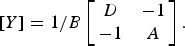 $$\left[Y \right]=1/B\left[{\matrix{ D & { - 1} \cr { - 1} & A \cr } } \right].$$
Also the S 21 parameters can be written as [Reference Pozar18]
 $$S_{21}=\displaystyle{{ - 2Y_{21} Y_0 } \over {\lpar Y_0+Y_{11} \rpar \lpar Y_0+Y_{22} \rpar - Y_{12} Y_{21} }}\comma \;$$
where is Y 0 the feed line characteristic admittance and S 21 can be determined from (1) to (3). However, the detailed analytical expression of S 21 is complicated. Figure 3 shows its calculated transfer characteristic against the simulated ones. It is evident that a good consistency between these two responses is observed, confirming the validity of the proposed filter model correctness.
Fig. 3. Transfer characteristics of the basic designed filter.
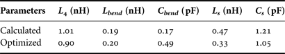
Figure 4 shows the simulated frequency-dependent transmission response of the basic structure. It can be seen that it has transmission poles distributed around high frequencies, which can be used to achieve wide bandpass. We also can see in this figure that by decreasing the C bend from 0.58 to 0.45 pF, transmission poles are shifted, providing the transmission poles in the desired frequencies. The calculated and optimized values for L–C equivalent circuit are summarized in Table 1.
Fig. 4. Simulated S 21 of the basic structure UWB BPF with varied C bend.
Table 1. Element values used in the equivalent circuit of the basic designed filter.
The optimized dimensions in Fig. 2 are W 1 = 9.24 mm, W 3,4 = 2.18 mm, l 1 = 3.12 mm, l 3 = 0.67 mm, and l 4 = 4.84 mm.
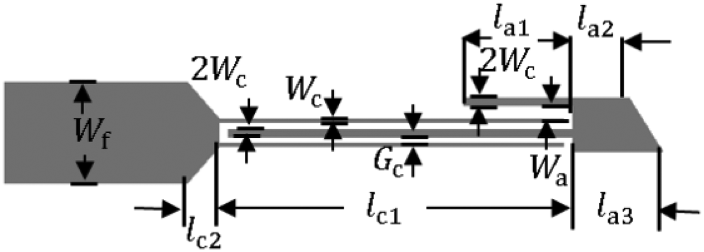
In more literatures such as [Reference Wu, Chen and Chen6, Reference Nakhlestani and Hakimi19–Reference Xu, Wu, Kang and Miao22], interdigital coupled lines have been widely used as a capacitive coupling element in bandpass filters. If this modified SIR is properly fed with two interdigital parallel-coupled lines with an increased coupling degree as shown in Fig. 5, an UWB passband can be made up. Like [Reference Xu, Wu, Kang and Miao22], in order to achieve a tight coupling and lower insertion, both strip and slot at interdigital coupled lines are reduced. The idea of using small lines in interdigital coupled lines has been extracted from [Reference Zhang and Xiao5] to achieve more coupled and improve frequency response. Considering the tight coupling required and the PCB design rules specified, the dimensions in the interdigital coupled lines are chosen as W C = 0.1 mm, G C = 0.1 mm, W a = 0.29 mm, W f = 2.42 mm, l C1 = 8.39 mm, l C2 = 0.76 mm, l a1 = 2.59 mm, l a2 = 1.37 mm, and l a3 = 2.18 mm as illustrated in Fig. 5.
Fig. 5. Interdigital coupled lines.
It can be clearly observed from Fig. 6 that by replacing right angles with rounded angles, the transition losses will better in the passband [Reference Wadell23].
Fig. 6. (a) Layout and (b) S-parameters of modified SIR.
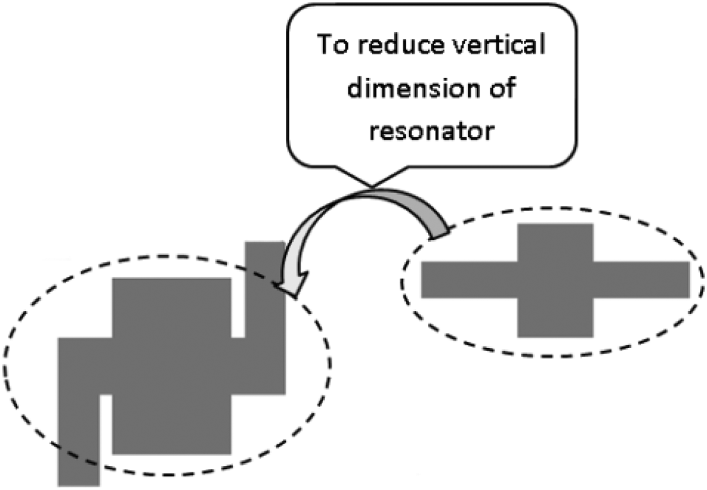
In order to improve the passband performances, rectangular slots were proposed as shown in Fig. 7. Also using rectangular slots can be modified the performances, while at the same time the whole circuit area will be more compact.
Fig. 7. (a) Layout and (b) S-parameters of modified SIR with rectangular slots.
The optimized rectangular slot dimensions are as follows: l S (the length of all rectangular slots) = 0.27 mm, l d (the distance between rectangular slots) = 0.54 mm, W S1 = 8.12 mm, W S2 = 1.37 mm, W S3 = 4.79 mm, W S4 = 1.72 mm, D 1 = 0.95 mm, and D 2 = 0.7 mm. Moreover, the use of ring slots in SIR and feed lines has ability to effectively improve the pass-band characteristics and stop-band width as shown in Fig. 8 because the current densities cannot pass through the resonator but stop at the slot.
Fig. 8. (a) Configuration and (b) S-parameters of the proposed UWB filter.
Figure 9 shows the current densities of resonators about 2f 0 (stop-band frequency). We can notice that in Fig. 9(a) the current densities pass through the resonator. For the resonator in Fig. 9(b) the current densities cannot pass through the resonator but stop at the slot. The ring slot dimensions are slightly adjusted as W r (the width of all ring slots) = 0.15 mm, W r1 = 0.27 mm, W r2 = 0.35 mm, l r1 = 5.56 mm, l r2 = 1 mm, l r3 = 1.45 mm, l r4 = 0.96 mm, l r5 = 0.94 mm, l r6 = 2.92 mm, l r7 = 0.76 mm, l r8 = 3.61 mm, D 3 = 0.71 mm, D 4 = 0.51 mm, and D 5 = 1 mm.
Fig. 9. Current densities of resonator (a) SIR resonator and (b) slotted stepped-impedance resonator (SSIR).
III. UWB BPF WITH A NOTCHED BAND
The next step after achieving wide passband from 3.11 to 10.65 GHz is to provide notched band in order to suppress undesired signals. Here by loading spiral slot on ground structure without any change in SR structure as shown in Fig. 10, a transmission zero (TZ) is created, which can be exploited for producing notch in passband. Figure 11 shows that by increasing physical dimensions as S G, D G, and l G in defected ground structure (DGS) by a factor of x = 5%, the center frequency of the notched band moves from higher band to the lower ones. With select the S G = 0.26 mm, D G = 0.24 mm, and l G = 0.73 mm, we can make the notch band in 8 GHz. It is clear from the results, that the notched-band response can be independently controlled only by varying the DGS, while the main physical dimensions of SR UWB BPF do not changed, which indicates a good way for controllable notched-band design procedure to suppress any unwanted frequencies in the passband.
Fig. 10. (a) Topology of the SDGS and (b) full-wave simulated response of the SDGS.
Fig. 11. (a) Layout and (b) simulated S 21 of the UWB BPF with a notched band for different dimensions of the SDGS.
IV. SIMULATION AND MEASUREMENT RESULTS
The EM simulations and optimizations for the BPF were performed using full-wave EM-simulator (ADS). Figures 12(a) and 12(b) present the simulated/measured S-parameters of the designed SR UWB filter and photograph of the fabricated filter. The fabricated UWB BPF has a wide −3 dB bandwidth more than 7.54 GHz, i.e. from 3.11 to 10.65 GHz (which satisfies the requirements of FCC-specified UWB limits) and a wide upper stopband that extends up to 16 GHz with high attenuation (−20 to −50 dB). For this filter, the return loss is better than 11 dB in 85% of pass-band width, whereas the insertion loss is less than 0.6 dB. Figures 13(a) and 13(b) present the photograph and EM simulated/measured S-parameters of the designed SR UWB BPF with a notched band, respectively. The measured −3 dB bandwidth of the filter is from 3.06 to 10.58 GHz including a notched band centered at 8.07 GHz that shown this filter can satisfy the FCC's requirements better than the filters introduced in [Reference Zhang and Xiao5, Reference Wadell23–Reference Lee, Hsu and Chen25].
Fig. 12. Fabricated SSIR UWB BPF. (a) Simulated and measured S-parameters and (b) photograph.
Fig. 13. Fabricated UWB BPF with a notched band (a) simulated and measured S-parameters and (b) photograph.
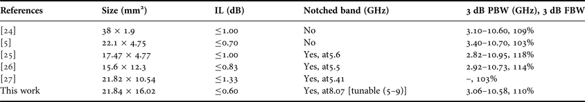
The insertion loss including the loss of a pair of the SMA connectors is about 0.6 dB, which is improved in comparison with designs presented in [Reference Zhang and Xiao5, Reference Fallahzadeh and Tayarani24–Reference Kim and Chang27]. The overall size of the fabricated UWB BPF is about 21.84 × 16.02 mm, which corresponds to an electrical size of 0.68 λg × 0.5 λg, where λg is the guided wavelength at the center frequency. Table 2 gives the comparison of designed SR UWB BPF with a notched band with a number of previously reported UWB BPF designs. As a result, the insertion loss and FBW are better than the other, while presenting a novel notched-band technique.
Table 2. Performance comparisons among published filters and the proposed one
IL, insertion loss; PBW, pass-band bandwidth; FBW, fractional bandwidth.
V. CONCLUSION
In this paper, two compact UWB BPFs with and without a notched band using the proposed SR and SDGS are proposed and fabricated. The generated notched band can be independently controlled by varying the dimensions of SDGS without any change in UWB BPF structure. Also the method of ABCD matrix calculating for prototype filter is provided. Two fabricated filters have low insertion loss, simple structure, and compact size that these performances are very attractive in the practical UWB applications in communication systems.
Gholamreza Karimi was born in Kermanshah, Iran in 1977. He received his B.S., M.S., and Ph.D. degrees in Electrical Engineering from Iran University of Science and Technology (IUST) in 1999, 2001, and 2006, respectively. He is currently an Assistant Professor in Electrical Department at Razi University, Kermanshah, since 2007. His research interests include low-power Analog and Digital IC design, RF IC design, modeling and simulation of RF-mixed signal IC, and microwave devices.
Farnaz Khamin Hamedani was born in Kermanshah, Iran in 1980. She received her B.Sc. degree in Electronic Engineering in 2003 from Razi University, Kermanshah, Iran and M.Sc. degree in Electronic Engineering in 2013 from Kermanshah Science and Research Branch, Islamic Azad University, Kermanshah, Iran. Her current research interests are focused on RF/Microwave circuit design.
Hesam Siahkamari was born in Kermanshah, Iran in 1988. He received his B.Sc. degree in Electronic Engineering in 2010 from Islamic Azad University, Kermanshah Branch, Kermanshah, Iran and M.Sc. degree in Electronic Engineering in 2013 from Razi University, Kermanshah, Iran. His current research interests are focused on RF/Microwave circuit design.