Introduction
The promising potential of ultra-wideband (UWB) technology compelled the Federal Communications Commission (FCC) to release the unlicensed frequency spectrum of 3.1–10.6 GHz for handheld devices used in short-range communications [1]. An essential component in the UWB system is the UWB bandpass filter (BPF), which keeps in check the prescribed bandwidth. The UWB-BPF, unlike the narrow BPF, has much mature theory involved in its design. Modern technologies like multiple mode resonators (MMR)/stepped impedance resonator (SIR) [Reference Zhu, Sun and Menzel2, Reference Zhang and Xiao3], cascaded broadband highpass and lowpass filters [Reference Hsu, Hsu and Kuo4, Reference Tang and Chen5], surface-to-surface broadside coupled structures (microstrip-to-coplanar waveguide (CPW)) have exhaustively been used in the design of UWB-BPFs [Reference Wang and Zhu6, Reference Wang, Zhu and Menzel7]. The microstrip-to-CPW-based UWB filters, compared with the rest, have minimum insertion loss response in the passband due to the tight broadside coupling of the structure [Reference Wang and Zhu6]. However, most of the UWB filters are susceptible to interferences from other wireless services.
The emission mask (−75 dBm/MHz) prescribed by the FCC for UWB systems in indoor environment prohibits them from acting as sources of interference to other in-band wireless services like WLAN, C band, X band, etc.. However, these RF services radiate a substantial amount of power in their domain of operation thereby creating significant interference to the UWB systems. The viable solution to the above-mentioned problem is UWB filters with integrated bandstop characteristics. This necessity led to an exhaustive amount of research into the design and development of multi-notched band UWB filters [Reference Deng, Zhao, He, Jia and Wang8–Reference Ghazali and Pal15]. An UWB filter based on folded triple-mode slotline resonator and microstrip–slotline transition implements dual notch using the inverse quarter wave resonators (QWRs) coupling stepped impedance microstrip stub that generates multiple TZs [Reference Deng, Zhao, He, Jia and Wang8]. A dual notched band filter is proposed wherein notched bands are obtained using the meander slot line and by folding one coupling arm of the UWB filter [Reference Song, Yang and Geyi9]. In [Reference Sarkar, Ghatak, Pal and Poddar10] dual notched band is implemented using a couple of spiral slotline resonators in ground and an inward folded resonator on the top. Another dual band-notched UWB-BPF has multiple split ring resonators (SRR) on top and a spiral-shaped defected ground structure (SDGS) in CPW on ground [Reference Ghazali, Sazid and Pal11]. A triple notched band UWB-BPF using triple mode SIR is reported in [Reference Wei, Li, Shi and Huang12], wherein the triple mode resonator is equivalent to three shunt-connected series LC resonance circuit which generates the triple notch. An UWB BPF comprising of four folded shunt quarter-wavelength short-circuited stubs with triple notched bands is proposed in [Reference Wei, Wang, Yang and Shi13]. Another triple notched band UWB filter on an E shaped MMR with three parallel U-shaped defected microstrip slots is reported in [Reference Wang, Zhao and Li14]. Three defected ground structures (DGS) embedded in the MMR based CPW implements triple notch in [Reference Ghazali and Pal15]. However, all the above triple notched structures are large in size and most of them do not show significant stopband extension.
In this manuscript we propose a compact UWB-BPF with the triple notched band and simultaneously widened upper stopband. Here we have considered the principle of back-to-back microstrip-to-CPW [Reference Wang and Zhu6] based UWB filter to design our basic filter because of its inherent strong coupling and smooth passband response. Into this basic structure two λ g/4 open circuited stubs and two complementary SRR (CSRR)-type DGS are embedded to generate triple stopbands in the UWB spectrum. The notch frequency position is a function of open-circuited stubs and CSRR profile dimension. The commercial, full-wave electromagnetic (EM) simulation software, IE3D is used to design the proposed UWB-BPF and the prototype is fabricated on RT/Duroid 6010 substrate of dielectric constant 10.8, loss tangent 0.0023 and thickness 0.635 mm.
Design of basic UWB filter
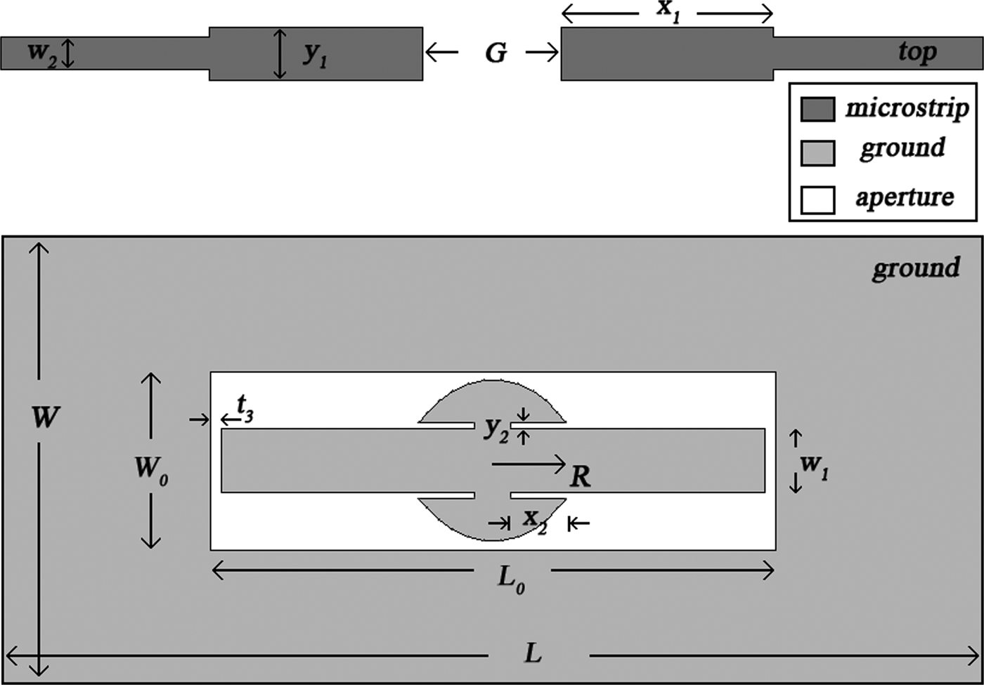
The proposed filter's design methodology is based on microstrip-to-CPW technique, wherein two microstrip lines on the top are arranged in back-to-back fashion and coupled to the MMR (embedded in the CPW) on the ground through the common dielectric layer, as shown in Fig. 1. The open circuited MMR used here is a modified SIR with the circular central section of radius R and two rectangular arms at either ends of width w 1 each, where R > w 1.

Fig. 1. Architecture of the basic microstrip-to-CPW transition-based UWB filter. Dark and light gray shade is conductor whereas white shade is aperture. All dimensions in mm.
The SIR has resonant modes whose position is a function of SIR dimensions. In order to map the entire UWB spectrum, these resonant modes must be placed approximately quasi-equally within the UWB passband. The resonance response of the SIR alone can be achieved when there is no coupling present between the MMR in the ground plane and microstrip lines on the top plane. This kind of coupling is referred to here as “weak coupling’. Figure 2 depicts the positions of resonant modes for fixed w 1 = 1.12 mm and variable R under weak coupling cases. It can be observed from Fig. 2 that the position of first resonant mode (f 1) remains almost fixed (at 3.5 GHz) whereas the higher resonant modes (f 2, f 3) shift considerably with variation in R. For an optimized value of R = 1.4 mm, the resonant modes are found to be approximately quasi-equally located from each other in the UWB passband, i.e., at 3.6, 6.65, and 9.95 GHz, respectively.
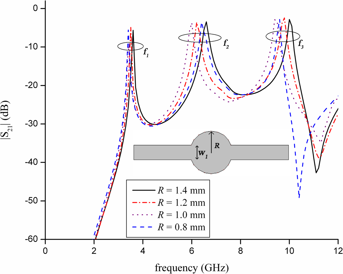
Fig. 2. Resonant modes of the modified MMR (SIR), with fixed w 1 = 1.12 mm and variable R, for weak coupling cases.”
The next step involves optimizing the coupling of surface-to-surface transition so as to simultaneously excite the resonant modes and generate the requisite UWB passband. To realize a practical UWB filter this transition is required to be strongly and efficiently coupled. This sort of coupling is termed here as “tight coupling’. The transition consists of two microstrip conductors on top (arranged in a back-to-back manner) electrically coupled to the SIR-based CPW in the ground. Figure 3 depicts the coupled section of the UWB filter. The coupling of transition is capacitive in nature and is characterized by an equivalent unified J-inverter network [Reference Wang, Zhu and Menzel7]. The J-inverter admittance represents the capacitive coupling extent. In order to achieve maximum coupling at the central UWB frequency, length of coupled section (l 1) is optimized close to λ g/4, and widths of MMR and microstrip (w 1, y1) are tuned accordingly. This tight electromagnetic coupling (EM) of the transition reduces the parasitic radiation loss [Reference Wang, Zhu and Menzel7].

Fig. 3. Schematics of the coupled section (Microstrip lines on the top coupled to narrow rectangular arms of the MMR in ground).”
Four rectangular slits (fixed width y 2 = 0.1 mm and variable length, x 2) etched at the junctions of circular and rectangular section of the MMR (depicted in Fig. 1) improves the impedance matching between them which maximizes the return loss (<−16 dB) and minimizes insertion loss (>−0.34 dB), as depicted in Fig. 4. Finally, the S parameters are obtained for optimized (manually) dimensions of the basic UWB filter, Fig. 5, wherein it can be observed that the four pole filter has passband extending from 3 to 10.9 GHz with 3 dB fractional bandwidth (FBW) of 113%, and an extended stopband till 15 GHz with attenuation <−18 dB. The optimized dimensions of the basic UWB filter are L = 17.82 mm, W = 11.08 mm, L 0 = 9.82 mm, W 0 = 3.08 mm, R = 1.4 mm, x 1 = 3.7 mm, y 1 = 0.92 mm, w 1 = 1.12 mm, x 2 = 0.56 mm, y 2 = 0.1 mm, w 2 = 0.56 mm, t 3 = 0.19 mm, G = 2.4 mm.
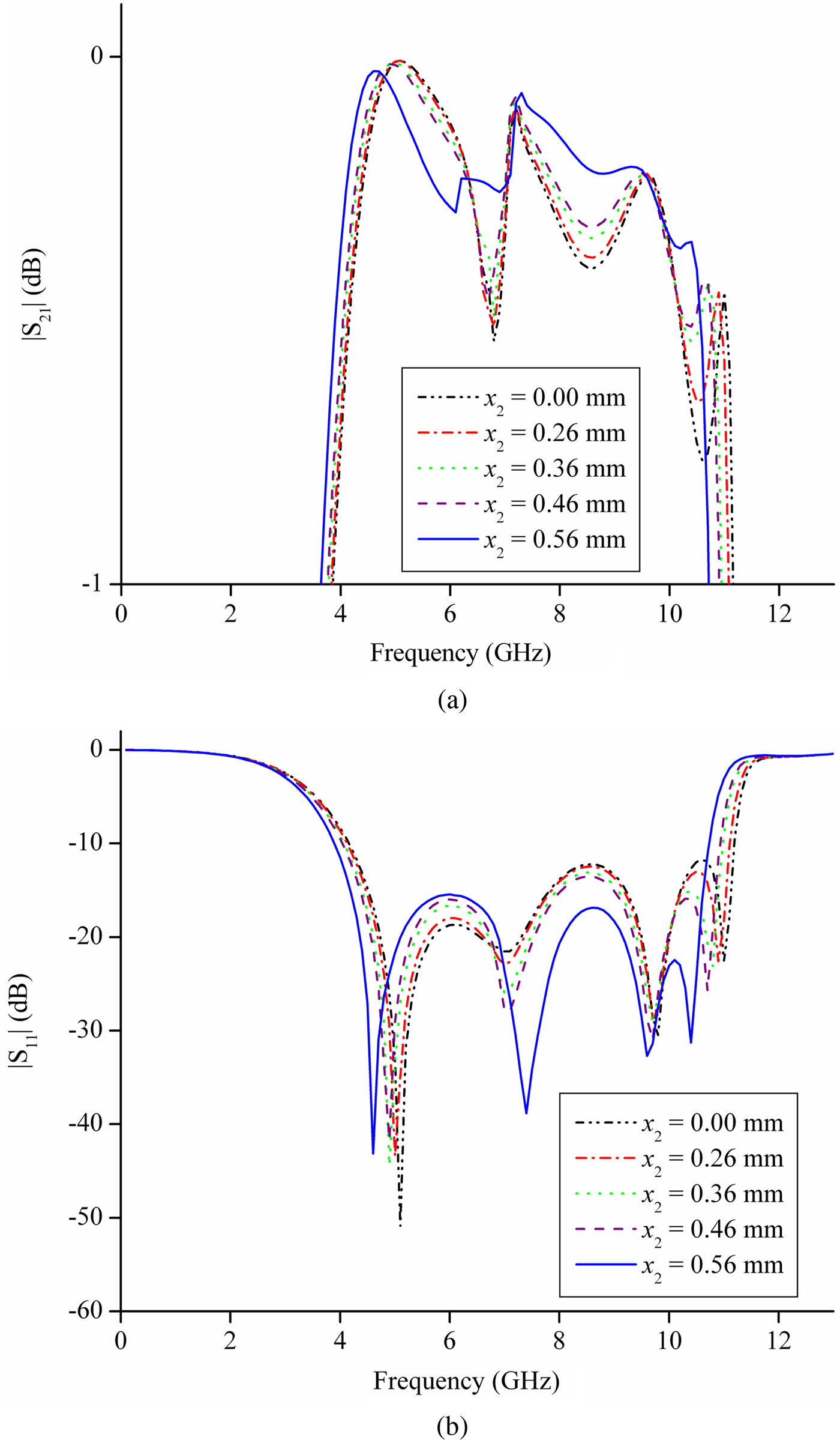
Fig. 4. Comparative S parameters for fixed width y 2 = 0.1 mm and variable length, x 2, of slit.
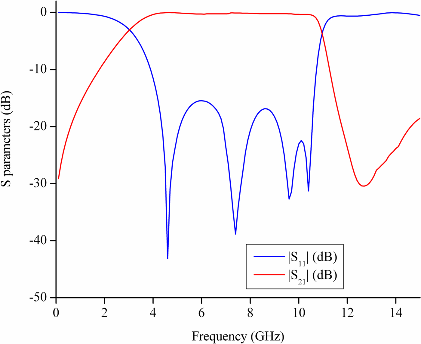
Fig. 5. Optimized frequency characteristics of the basic UWB filter.
Band notched UWB filter
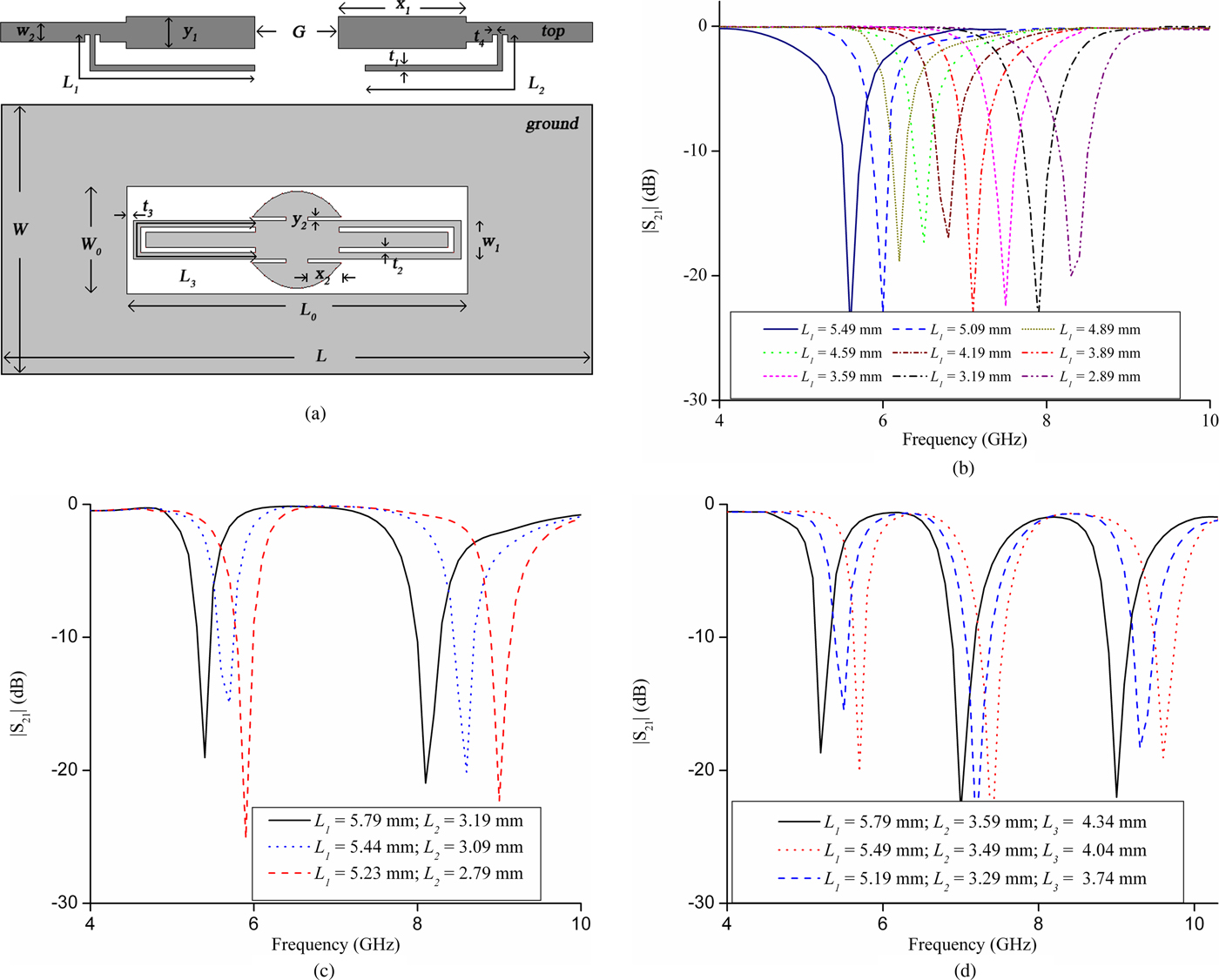
The indoor operation of UWB systems is susceptible to interference from other RF wireless services like WLAN, C band etc., which can seriously hamper their performance. To circumvent these interferences UWB filters with integrated multiple stopband characteristics were proposed [Reference Deng, Zhao, He, Jia and Wang8–Reference Ghazali and Pal15]. Here we introduce notches in the passband using open circuited stubs and DGS. The stubs and DGS, embedded into the basic UWB filter (Fig. 6(a)), generate TZs which are placed in the passband at frequencies of interest in order to mitigate interference. Single (dual) passband notch(es) are introduced by the TZ of open-circuited stubs, wherein the notch resonant frequency is related to lengths of stubs via the formula
 $$f_{notch}\approx \displaystyle{c \over {4L_{stub}\sqrt {\varepsilon _{reff}_{}}}}, L_{stub} = {\rm} L_1,{\rm} L_2,$$
where c is the speed of light, ε reff is the effective dielectric constant and L stub is the length of stubs, L 1, L 2. That is to say, stubs are approximately quarter wavelength resonators.

Fig. 6. (a) Layout of the proposed triple notched band UWB filter. L = 17.82 mm, W = 11.08 mm, L 0 = 9.82 mm, W 0 = 3.08 mm, R = 1.4 mm, x 1 = 3.7 mm, y 1 = 0.92 mm, w 1 = 1.12 mm, x 2 = 0.56 mm, y 2 = 0.1 mm, w 2 = 0.56 mm, t 1 = 0.15 mm, t 2 = 0.15 mm, t 3 = 0.19 mm, t 4 = 0.2 mm, L 1 = 5.69 mm, L 2 = 4.89 mm, L 3 = 7.36 mm G = 2.4 mm. Controllable notches for variable lengths of (b) single stub (c) dual stub (d) stubs and CSRR.
Similarly, it is seen that the CSRR DGS is a half wavelength resonator, wherein the notch resonant frequency is given by
 $$f_{notch}\approx \displaystyle{c \over {2L_{CSRR}\sqrt {\varepsilon _{reff}_{}}}}, \,L_{CSRR} = L_3.$$
Figures 6(b and c) represent controllable notches for variable length (L 1/L 2) of the stub. In order to introduce the third notch, complementary split ring resonator (CSRR) type DGSs are embedded into the narrow rectangular arms of the MMR in the ground. Figure 6(d) depicts controllable triple passband notches for variable lengths of stubs and CSRR (L 3).
The frequency response of the proposed structure is depicted in Fig. 7(a) wherein the two notches at 5.2 and 6.1 GHz (so as to eliminate interference from WLAN and C band) are the result of TZs due to the dual stubs. The CSRR generates TZ at 8.1 GHz in order to eliminate interference of X band. Also, it can be observed that the passband exists from 3 to 10.9 GHz with stopband extended till 15 GHz and having attenuation <−17 dB. These frequencies have been selected for depicting the application of the filter in interfering environments. Other frequencies like WLAN (5.8 GHz), RFID (6.5 GHz), etc., could very well have been chosen. In general, the proposed design can place TZ at any possible frequency in the passband by simply adjusting the dimensions of the stubs and CSRRs. Also, the proposed structure can develop a maximum of three notch frequencies. If we try for the fourth notch, then the return loss between third and fourth notch degrades significantly. The filter has been designed keeping in mind the tolerance of the manufacturing process. For e.g., the widths of conductors {stubs (t 1) and microstrip lines} have not been taken too thin (at least 0.1 mm). Also, the widths of slots (t 2, t 3, t 4, y 2) are not reduced below 0.1 mm. Figures 7(b–d) display the current distribution in the proposed structure at 5.2, 6.1, and 8.1 GHz, respectively. The figures clearly depict the coupling of stubs and CSRRs to the basic UWB filter at their respective resonant frequencies.
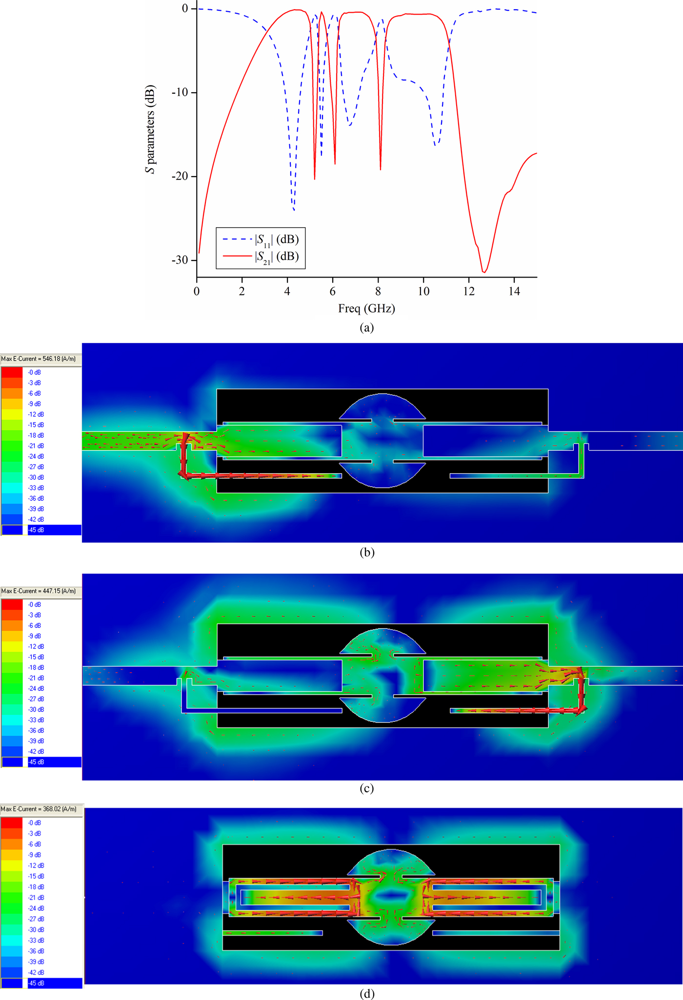
Fig. 7. (a) Frequency characteristics of the proposed UWB filter. Current distribution at the three-notch frequencies, (b) 5.2 GHz, (c) 6.1 GHz, and (d) 8.1 GHz.
Measurement and results
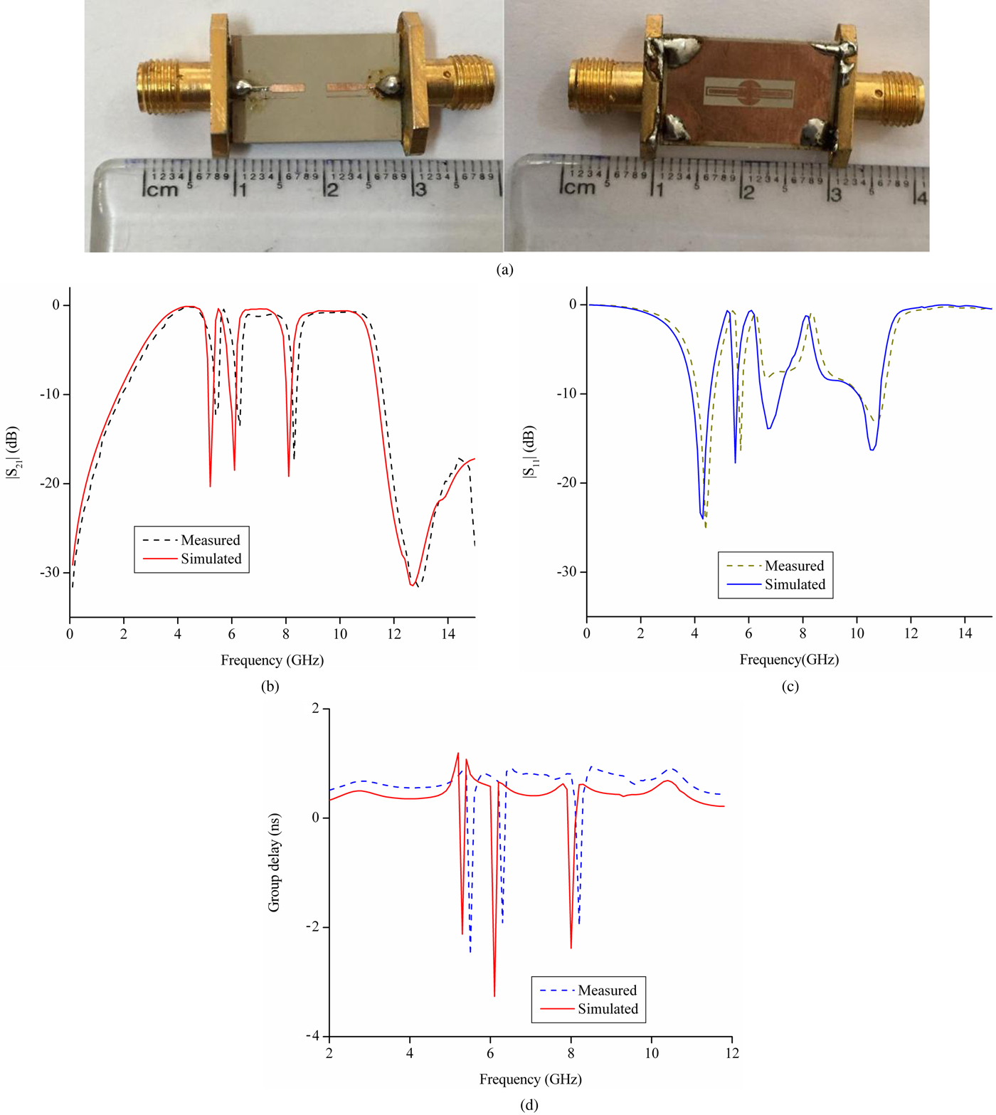
Figure 8(a) depicts the picture of the fabricated prototype, whereas the comparative simulated and measured results of the fabricated UWB filter are shown in Figs 8(b–d).

Fig. 8. (a) Picture of the fabricated filter. (b) Comparative measured and simulated |S 21|. (c) Comparative measured and simulated |S 11|. (d) Comparative measured and simulated group delay.
The measurement of the structure is done using Agilent vector network analyzer N5230A. The measured response exhibits passband from 3.15 to 11.1 GHz and triple notched bands at 5.3, 6.25, and 8.28 GHz, respectively. The stopband is deeper than −17 dB from 11.1 to 15 GHz. Each notched band has an attenuation level <−13 dB, whereas the 3 dB FBW observed is about 4.03, 4.12, and 3.87% at 5.3, 6.25, and 8.28 GHz, respectively. The maximum insertion loss observed in the passband before the first notch is −0.4 dB, between first and second notch it is −0.56 dB, between second and third notch it is −0.85 dB and after the third notch it is −0.62 dB. The variation in group delay is <0.17 ns in the whole band except at the notched bands. The deviation of measured results from simulation may be due to the loss tangent of the substrate, parasitic effects of the SMA connectors and other uncertain phenomenon. Table 1 provides a comparative illustration of the proposed structure with recent triple notched band UWB filters. It can be observed from Table 1 that the proposed structure has a better stopband response than all except [Reference Ghazali and Pal15]. Also, the proposed structure is comparable in size with all the proposed triple notched band UWB filters.
Table 1. Comparison of the proposed structure with recent triple notched band UWB filters

Conclusion
This paper proposes a compact triple notched band UWB with extended stopband. The basic UWB filter consists of circular MMR based CPW in the ground coupled to microstrip lines in the top. The passband encompasses the requisite UWB and the stopband is wide and deep till 15 GHz. Open circuited stubs coupled to the microstrip lines and CSRR based DGS embedded in the narrow arm of MMR, of the basic UWB filter, generates triple notches at 5.2, 6.1, and 8.1 GHz, respectively. Also, the group delay variation is minimal in the passband. Owing to its compact size and satisfactory passband and stopband performances, the proposed structure is attractive for integration into UWB systems.
Author ORCIDs
Abu Ghazali, 0000-0001-9689-8545
 Abu Nasar Ghazali received his B.Tech degree in Electronics & Communication Engineering (ECE) from SRM University, Chennai, in 2008 and M.E degree in Microwave Engineering from Birla Institute of Technology (BIT) Mesra, in 2010 where he was a GATE scholar. He completed his doctorate in 2014 from BIT Mesra. He worked as an Assistant Professor (I) in the Dept. of ECE at the BIT Mesra, Patna campus. Currently he is an Assistant Professor (II) in the School of Electronics Engineering, at the Kalinga Institute of Industrial Technology (KIIT), Deemed University, Bhubaneswar, India. He is an Associate member, The Institution of Engineers (IEI), India and member of IEEE. He has published quite a few papers in SCI/SCOPUS indexed journals and conferences. His main research interests are UWB filters, Microstrip filters and passive microwave circuit components.
 Jabir Hussain received his B.Tech degree in Electronics and Telecommunication from Assam Engineering College in 2009 and M.Tech degree in RF and Microwave Engineering from IIT Kharagpur in 2016 where he was a GATE scholar. He is currently working as an Assistant Professor in the School of Electronics Engineering at KIIT Deemed University, Bhubaneswar, India. His research interests include Microstrip-based circuit, microstrip filters and mixed-signal design.
 Srikanta Pal received his B.Tech degree in Electronics & Communication Engineering from NIT Warangal, India and M.Tech degree in Microwave Engineering from Jadavpur University, India in 1990 and 1992, respectively. From 1992 to 2000 he was with the R&D Antenna Lab of the Bharat Electronics Limited (BEL). In 2001 he joined the Oxford University as a Research Associate where he worked towards his Ph.D. on HTS Microwave Filters, which he completed in 2003. From 2003 to 2005 he was a Visiting Faculty in the Centre for Advanced Research in Electronics (CARE) Dept. at the IIT Delhi, India. In 2005 he joined the Dept. of Electronics and Computer Engineering at the IIT Roorkee, India, as an Assistant Professor. He joined the Emerging Devices Technology center at the Birmingham University as a Post Doctorate fellow in 2006 where he designed a HTS filter which is currently installed in the world's largest Telescope, Green Bank Telescope (GBT), West Virginia, USA. In 2008 he joined the ECE Dept. at the BIT Mesra as an Associate Professor and currently is working as a Professor and Head of the Department. He is also a lifetime Research Fellow at the University of Birmingham. His research interests include RF Filters and Devices, MEMS, HTS Microwave filters, Antennas and Computational Electromagnetics.