


I. INTRODUCTION
Poly(methyl methacrylate) (PMMA) is one of the most important polymers for application as dielectric layer in organic electronics devices, e.g. in organic field-effect transistors (OFETs) (Veres et al., Reference Veres, Ogier and Lloyd2004). The gate dielectric layer has a significant impact on the performance of OFETs. Its interface to the semiconductor strongly influences the charge carrier mobility in the transistor channel because at this interface charges are accumulated and move (Sze and Ng, Reference Sze and Ng2006). Therefore, the order in the semiconductor/dielectric interface plays an important role.
The present study aimed at a better understanding of the order and self-organization behavior of PMMA-based dielectric polymers. The polymers chosen were designed to support the self-organization of the semiconductor polymer by self-organization of the dielectric layer, a concept is already proposed in the literature (Jurchescu et al., Reference Jurchescu, Popinciuc, van Wees and Palstra2007; Ito et al., Reference Ito, Virkar, Mannsfeld, Oh, Toney, Locklin and Bao2009; Miozzo et al., Reference Miozzo, Yassar and Horowitz2010).
The polymers studied here were random terpolymers of methyl methacrylate (methyl MA; MMA), a crosslinking monomer (BP: 4-benzoylphenyl MA; BP-C6: 6-[(4-benzoylphenyl)oxy]hex-1-yl MA; Pg: prop-2-yn-1-yl MA (propargyl MA); or Pg-C6: 6-[(prop-2-yn-1-yl)oxy]hex-1-yl MA), and a semifluorinated methacrylate (sfMA). Semifluorinated poly(methacrylate)s were already demonstrated to show self-organization by the formation of ordered layers (Pospiech and Jehnichen, Reference Pospiech, Jehnichen, Smith, Iacono and Iyer2014; Pospiech et al., Reference Pospiech, Jehnichen, Chunsod, Friedel, Simon, Grundke, Ameduri and Sawada2016). The strength of the self-organization depends on the length of the semifluorinated (sf) side chains. In the terpolymers studied here, these subunits were randomly distributed, as illustrated in the chemical structure given in Figure 1. SfMA monomers with systematically varied sf substituents (-O-(CH2)10-(CF2)10F, -O-(CH2)2-(CF2)8F or -O-(CH2)2-(CF2)6F) were incorporated into the terpolymers. The synthesis has been described before (Berndt et al., Reference Berndt, Pospiech, Jehnichen, Häußler, Voit, Al-Hussein, Plötner, Kumar and Fischer2015; Al-Hussein et al., Reference Al-Hussein, Berndt, Jehnichen, Häußler, Stamm and Pospiech2016).

Figure 1. Chemical structure of the MMA copolymers used as dielectric layer. With BP: 4-benzoylphenyl; BP-C6: 6-[(4-benzoylphenyl)oxy]hex-1-yl; Pg: prop-2-yn-1-yl (propargyl); Pg-C6: 6-[(prop-2-yn-1-yl)oxy]hex-1-yl.
The effect of the length of the side chain and concentration in the terpolymer was investigated. In the first step, the bulk structure of the polymers after synthesis was examined by wide-angle X-ray scattering (WAXS). The information gained from the bulk is essential to estimate the expectations for the structure generation in thin films. Only terpolymers that generate an ordered structure in bulk can form an ordered structure in thin films. Thin films were prepared by spin-coating onto silicon wafers. The ordering behavior of the sf units in the dielectric layers was studied by a combination of methods. Thin films (single films of dielectric, double layers of dielectric on the semiconductor layer) were investigated by X-ray reflectometry (XRR). As semiconductor, poly(3-hexylthiophene-2,5-diyl) (P3HT) was employed.
The results of the study will be used to select polymer compositions suitable for self-organized dielectric layers in OFETs.
II. EXPERIMENTAL
A. Sample preparation
1. Materials
The following solvents were employed for thin film preparation: chloroform (CHCl3, >99%, Sigma-Aldrich), octadecafluorooctane (perfluorooctane, PFO, 98%, Sigma-Aldrich), 1,3-bis(trifluoromethyl)benzene (BFMB, 99%, Aldrich). The semiconductor poly(3-hexylthiophene-2,5-diyl) (P3HT, regioregular) was purchased from Sigma-Aldrich.
2. Copolymer synthesis
The random copolymers studied were synthesized by radical copolymerization in solution as reported before (Berndt et al., Reference Berndt, Pospiech, Jehnichen, Häußler, Voit, Al-Hussein, Plötner, Kumar and Fischer2015; Berndt, Reference Berndt2016).
3. Film preparation
The silicon wafers were pre-cleaned in a mixture of H2O2 : NH4OH : H2O (4 : 1 : 1 vol/vol/vol) at 80 °C for 0.5 h followed by thorough rinsing with deionized water, drying with nitrogen flush and annealing under reduced pressure at 100 °C for 2 h. Thin films were prepared by spin-coating of diluted polymer solutions in PFO or BFMB (polymer concentrations usually 1 wt.% except for experiments where the film thickness was varied) and subsequently dried under reduced pressure (50 °C, overnight). Crosslinking was realized either by UV irradiation (BP-containing copolymers) or by annealing at 130 °C in vacuum or argon atmosphere for different times (4 … 48 h) (Pg-containing copolymers).
B. X-ray scattering experiments
1. WAXS
WAXS was carried out at 2-circle diffractometer XRD 3003T/T (GE Sensing & Inspection Technologies, Ahrensburg, Germany) in symmetric step-scan mode with Δ2θ = 0.05° and t = 40 s (using CuKα radiation λ = 0.1542 nm (monochromatized by primary multilayer system) and slit geometry (0.2 mm/0.3 mm)). Scattering results were presented as log(I) vs. 2θ with vertically shifted curves for better visualization. To determine d-values fit procedures were executed applying the software tool Analyze (part of the control program Rayflex of the scattering device XRD 3003T/T).
2. XRR
XRR experiments were realized with the same diffractometer in symmetric step-scan mode with Δ2θ = 0.01° and t = 5 s with CuKα radiation λ = 0.1542 nm and slit geometry (0.05 mm/0.07 mm). Scattering results were presented as log(I) vs. 2θ with vertically shifted curves for better visualization. Calculations of film thicknesses f were performed with good quality using a linear regression over all minima in the XRR curve (Kiessig interferences). Owing to the architecture of the random copolymers consisting of three different subunits with different concentrations (compare Figure 1) a simple model of the film (e.g. averaged values for the refraction index or an appropriate layered structure) could not be applied. This model would become even more complex if areas of self-organized sf side chains are embedded in different arrangements. The layer thickness d sf-layer was determined in a similar manner as done for bulk samples.
III. RESULTS AND DISCUSSION
A. Ordering behavior of the copolymers in bulk
The formation of ordered structures in the bulk polymers was analyzed by WAXS. The as-synthesized copolymer powders were annealed above the glass transition temperature T g before analysis to improve the order. The information about the ordered structure (scattering curves, d-spacings) is required to understand the ordering behavior in thin films.
Three series of copolymers were studied (see Table I) having sf side chains of different length (-O-(CH2)10-(CF2)10F, abbreviated H10F10; -O-(CH2)2-(CF2)8F, abbreviated H2F8, and -O-(CH2)2-(CF2)6F, abbreviated H2F6). Based on the knowledge of the ordering behavior of other sfMA copolymers, it was expected that the copolymers with H10F10 side chains form a structure characterized by interdigitation of the sf side chains, while H2F8 and H2F6 copolymers would show a structure where the sf side chains arrange head-to-head (Jehnichen et al., Reference Jehnichen, Pospiech, Friedel and Funari2011; Jehnichen et al., Reference Jehnichen, Friedel, Selinger, Korwitz, Wengenmayr, Berndt and Pospiech2013; Pospiech and Jehnichen, Reference Pospiech, Jehnichen, Smith, Iacono and Iyer2014; Pospiech et al., Reference Pospiech, Jehnichen, Chunsod, Friedel, Simon, Grundke, Ameduri and Sawada2016).
Table I. Results of bulk investigations by WAXS and film investigations by XRR of random P(MMAm/XMAn/sfMA-HxFyo).

s – sharp reflection, b – broadened reflection, n – no reflection (amorphous maximum, only).
n.d. – not detectable. All samples were annealed for 4 h at 140 °C in a vacuum.
d sf-layer – caused by self-organizing of the sf side chains. f – film thickness.
d sfsc – side chain distance was determined assuming a pseudo-hexagonal lateral arrangement of the sf side chains (according to the hexagonal structure of PTFE (Yamamoto and Hara, Reference Yamamoto and Hara1982; Clark, Reference Clark1999)).
Prep. – conditions of film preparation.
*Solvent of spin-coating with polymer concentration of 1 wt.% and time of annealing at 140 °C in a vacuum. **Preparation of a film not possible. °Films prepared on wafer with additionally Al layer.
Self-organization in the sf side chain copolymers can be recognized by the generation of layer reflections. Well-ordered layer structures exhibit a number of reflection orders. Using Bragg's law and background corrected scattering curve the determination of the layer thickness d sf-layer could be done with good quality. This is illustrated in Figure 2 exemplarily for bulk sample H2F8-7. The fit procedure was executed by the software Analyze, including background correction, and resulting in the parameter output shown in Table II. Thus, the correct position of the Bragg reflections for the sf layers could be determined.
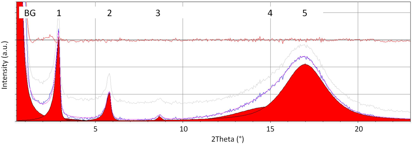
Figure 2. (Colour online) Determination of reflection positions d as demonstrated at bulk sample H2F8-7. BG – additional background (divergence of primary X-ray beam, tail of particle scattering); 1 – 1st order, 2 – 2nd order, 3 – 3rd order sf layer reflection; 4 – amorph. max. of mainly non-sf segments, 5 – amorph. max. of mainly sf segments. The fit procedure was executed applying the software tool Analyze (part of the control program Rayflex of the scattering device XRD 3003T/T) using pseudo-Voigt functions.
Table II. Determination of reflection positions d as demonstrated at bulk sample H2F8-7 using a fit procedure (compare Figure 2).

1 – 1st order, 2 – 2nd order, 3 – 3rd order sf layer reflection [→d sf-layer]; 4 – amorphous maximum of mainly non-sf segments, 5 – amorphous maximum of mainly sf segments [→d sfsc].
d_Fit – fitted d-value of reflections, 2th_Fit – fitted 2θ-value of reflections.
I −net and I −bg – linear net intensity height of reflections and their linear background intensity; FWHM – full width at half maximum of reflections; J −area – integral intensity of reflections.
The scattering behavior of the copolymer series is illustrated in Figure 3 (H10F10), Figure 4 (H2F8), and Figure 5 (H2F6), respectively. The WAXS curves of copolymers with sf side chains H10F10 (Figure 3) are characterized by reflections of a layer structure in the intermediate 2θ range (with a typical layer distance d sf-layer of about 5.00 nm), and in the wide angle range by a broad amorphous scattering behavior with one reflection representing the lateral ordering behavior of the sf side chains (with a typical side chain distance d sfsc of about 0.49 nm, which correlates well with the situation in poly(tetrafluoroethylene) (PTFE: a hex = 0.566 nm, d (100) = 0.490 nm or 2θ CuKα = 18.01°) (Yamamoto and Hara, Reference Yamamoto and Hara1982; Clark, Reference Clark1999). For detailed d-values see Table I.

Figure 3. (Colour online) WAXS patterns of random P(MMAm/XMAn/sfMA-H10F10o) with X = Pg, BP and variable m, n, and o. 1 – H10F10-1, BP/o = 36 mol%; 2 – H10F10-2, Pg/o = 56 mol%; 3 – H10F10-3, Pg/o = 41 mol%; 4 – H10F10-4, Pg/o = 36 mol%; 5 – H10F10-5, BP/o = 45 mol%. (For further details see Table I).

Figure 4. (Colour online) WAXS patterns of random P(MMAm/XMAn/sfMA-H2F8o) with X = Pg/Pg-C6 and variable m, n, and o. 1 – H2F8-1, Pg/o = 90 mol%; 2 – H2F8-3, Pg-C6/o = 90 mol%; 3 – H2F8-4, Pg-C6/o = 73 mol%; 4 – H2F8-5, Pg-C6/o = 56 mol%; 5 – H2F8-6, Pg-C6/o = 0 mol%. (For further details see Table I).

Figure 5. (Colour online) WAXS patterns of random P(MMAm/XMAn/sfMA-H2F6o) with X = Pg, BP and variable m, n, and o. 1 – H2F6-2, BP/o = 89 mol%; 2 – H2F6-3, Pg/o = 42 mol%; 3 – H2F6-1, BP/o = 100 mol%. (For further details see Table I).
In the case of copolymers with H2F8 side chains (Figure 4), the WAXS curves are characterized by reflections of the sf layer structure and by a broad amorphous scattering maximum. As expected in comparison to copolymers with H10F10 side chains, the typical layer distance d sf-layer was smaller with values of about 3.05 nm for high concentrations of sf side chains (90 and 73 mol% sfMA-H2F8). Smaller concentrations caused an enlargement of d sf-layer (to 3.30 nm for 56 mol%) and reduced the quality of the layer structure (reflection broadening and loss of higher reflection orders, i.e. in sample H2F8-5, Pg-C6). This was accompanied by the loss of the slightly sharper form of the amorphous maximum for copolymers with higher sf side chain concentration representing a near-order arrangement of the H2F8 side chains. The values d sf-layer for the side chain distance were between 0.516 and 0.53 nm, which are significantly larger, compared to PTFE. Sample H2F8-6, Pg-C6 (0 mol%), gave an impression about the overlapping of two amorphous scattering parts caused by the first and second segment (i.e. MMAm and XMAn, respectively) in the copolymer. Noticeable is the additional amorphous maximum at 2θ ~13° which could be found as the main scattering in PMMA homopolymer.
In Figure 5, the comparison of H2F6 side chain-containing copolymers is shown. A sf layer structure with reasonable quality could be detected only for the copolymer H2F6-2 (90 mol% sfMA-H2F6). Further decreasing of sf side chain concentration resulted again in a loss of the layer quality. In contrast to a comparable copolymer with H2F8 side chains (H2F8-5, Pg-C6; in Figure 4) the value of d sf-layer was decreased. The homopolymer H2F6-1 (100 mol%) offered a further reduced d sf-layer (see Table I).
As general result, both concentration as well as length of the sf substituent influenced the degree of order, i.e. the generation of layered structures as it was found in PMMA copolymers with H10F10-sfMA and H2F8-sfMA comonomers without crosslinking units (Jehnichen et al., Reference Jehnichen, Pospiech, Friedel and Funari2011; Jehnichen et al., Reference Jehnichen, Friedel, Selinger, Korwitz, Wengenmayr, Berndt and Pospiech2013; Berndt et al., Reference Berndt, Pospiech, Jehnichen, Häußler, Voit, Al-Hussein, Plötner, Kumar and Fischer2015; Pospiech et al., Reference Pospiech, Jehnichen, Chunsod, Friedel, Simon, Grundke, Ameduri and Sawada2016). The results summarized in Table I clearly reveal that the crosslinker used in the maximum concentration of 22 mol% in the copolymers and independent of its type (BPMA, PgMA or PgMA-C6 with hexyl spacer) had only a minor influence on the structure formation. The d-spacings relating to the layered structure of the sf side chains only depended on the length of the side chains: d sf-layer in the range of 4.9 nm refer to interdigitated H10F10 side chains (length of H10F10 side chain: 2.653 nm (Pospiech et al., Reference Pospiech, Jehnichen, Chunsod, Friedel, Simon, Grundke, Ameduri and Sawada2016)), d sf-layer in the range of 3.02–3.3 nm to H2F8 side chain layers arranged head-to-head (length of H2F8 side chain: 1.378 nm (Pospiech et al., Reference Pospiech, Jehnichen, Chunsod, Friedel, Simon, Grundke, Ameduri and Sawada2016)), and d sf-layer in the range of 2.4–3.09 nm to H2F6 side chains (length of H2F6 side chain: 1.114 nm (Pospiech et al., Reference Pospiech, Jehnichen, Chunsod, Friedel, Simon, Grundke, Ameduri and Sawada2016)). The driving force to ordering is weaker for shorter side chains, visible at the threshold comonomer concentration of sfMA that is necessary for structure formation (sfMA-H10F10: ~36 mol%; sfMA-H2F8: ~70 mol% without crosslinker, ~50 mol% with PgMA-C6 crosslinker; sfMA-H2F6: 90 mol%). The annealing effect of the improvement of the structure of the sf layers was found to be weak as well.
B. Thin film structure of dielectric layers
It was supposed that the length of the sf substituent, as well as their concentration, will determine the structure formation in thin films as in the bulk. For pre-evaluation of the films (e.g., determination of the film thickness, roughness), XRR investigations were performed. All XRR results of the dielectric films were collected in Table I, too.
In the first set, copolymer films with sfMA-H10F10 were examined. The XRR curves were compared in Figure 6. Here, all samples were prepared on Si wafers with additional Al layer (thickness 52.2 nm). The reason for this special substrate surface was to test the preparation of copolymer films on a metallic coating that is used for electric characterization (i.a., breakthrough voltage and threshold voltage in organic electronics). The assignment of the Kiessig interferences to the related sublayer (aluminum, copolymer) is not simple under the conditions of changing electron densities in the copolymer film (mainly because of the variation in the concentration of sf side chains) and the prepared thickness of the copolymer film f. The films exhibited f-values in the range of 40.0–58.7 nm.

Figure 6. (Colour online) XRR patterns of random P(MMAm/XMAn/sfMA-H10F10o) with X = Pg, BP and variable m, n, and o. 1 – H10F10-1, BP/o = 36 mol%; 2 – H10F10-2, Pg/o = 56 mol%; 3 – H10F10-3, Pg/o = 41 mol%; 4 – H10F10-4, Pg/o = 36 mol%; 5 – H10F10-5, BP/o = 45 mol%; 6 – wafer with additional aluminum layer. (For further details see Table I).
The layer structure caused by the H10F10 side chains was clearly visible and showed only a small dependency on the concentration of sfMA-H10F10. The range of d sf-layer was between 4.23 and 4.42 nm. But there is a significant lowering in the value of d sf-layer in thin films compared to the bulk (by around 0.45 nm in all bulk and film samples under investigation). This result should be regarded under the different history of the samples – synthesis conditions on the one side, and parameter of the film preparation on the other side. That means the conditions of layer generation were completely different. Furthermore, specific interactions play an important role under the confinement in thin films and centrifugal forces during the spin-coating. Thus, the tendency to a layer “compression” seems obvious.
The film thicknesses f were determined by plotting the position of the minima of Kiessig interferences vs. the number of the minimum, as illustrated in Figure 7 for film sample H2F8-4, giving the slope of the linear curve for calculation of f using Bragg's law. Superimposed layer reflections caused by the self-organization of the sf side chains were utilized for determinations of d sf-layer-values.

Figure 7. (Colour online) Plot of minima positions in the reflectometry curve of film sample H2F8-4 versus number of minimum and determination of the linear slope Δ2th. Using Bragg's law a simplified calculation of f could be executed (see results inserted in figure).
In Figure 8, the copolymers with H2F8 side chains were compared. The films with a very high concentration of sfMA-H2F8 (i.e. samples with 90 and 75 mol%) showed beside well pronounced Kiessig interferences layer reflections. A reduced concentration (50 mol%) hindered to generate a layer structure. Basing on these curves film thicknesses f in the range of 38.4–75.6 nm were calculated. The values of d sf-layer were only weak variable (from 2.91 to 2.94 nm). The tendency to reduce the values of d sf-layer compared to the bulk data were found here again. Only the mean difference step in relation to comparable sfMA-H10F10 films (viz. without sample with 56 mol%) was very small (0.13 nm, only). Besides the common discussion about the reason of the lowering (see above), an important difference in between both sf side chain interactions (H10F10 vs. H2F8) should be the other arrangement of the perfluorinated part of the side chains. In the case of H10F10 a strong interdigitation of this part is known and widely investigated, not only in MMA-based main chain copolymers (Pospiechet al., Reference Pospiech, Jehnichen, Chunsod, Friedel, Simon, Grundke, Ameduri and Sawada2016) but also in aromatic and semi-aromatic copolyesters with sf side chains (Friedel et al., Reference Friedel, Pospiech, Jehnichen, Bergmann and Ober2000; Jehnichen et al., Reference Jehnichen, Pospiech, Janke, Friedel, Häußler, Gottwald, Kummer, Kollig and Grundke2001; Gottwald et al., Reference Gottwald, Pospiech, Jehnichen, Häußler, Friedel, Pionteck, Stamm and Floudas2002), in sf side chain maleimide copolymers (Appelhans et al., Reference Appelhans, Wang, Zschoche, Zhuang, Häußler, Friedel, Simon, Jehnichen, Grundke, Eichhorn, Komber and Voit2005), and in sf side chain polysulfones (Tsuwi et al., Reference Tsuwi, Pospiech, Jehnichen, Häußler and Kremer2007). On the other side, at the same places, a head-to-head arrangement for H2F8 was discussed. This difference in arrangement should be also one of the main reasons for the scattering behavior in the wide-angle region: The strong generation of a PTFE-like (100) reflection verified the interdigitation over long perfluorinated side chain part (9–10 C atoms) with strong lateral interaction, whereas a shorter one (7–8 C atoms) is not able to perform that. A strong WAXS reflection could not be observed.

Figure 8. (Colour online) XRR patterns of random P(MMAm/XMAn/sfMA-H2F8o) with X = BP, BP-C6 and variable m, n, and o. 1 – H2F8-7, BP/o = 90 mol%; 2 – H2F8-8, BP-C6/o = 90 mol%; 3 – H2F8-9, BP-C6/o = 75 mol%; 4 – H2F8-11, BP-C6/o = 50 mol%. (For further details see Table I).
The results of the influence of different film preparation conditions on the formation of thin films and their ordering behavior are shown in Figure 9. The copolymer compositions chosen contained only sfMA-H2F6 as sf comonomer with two concentrations of 89 and 42 mol%, respectively. Variation parameters were the solvent for the copolymer solution and the annealing time of the spin-coated film. As expected because of the further shortening of the perfluorinated part of the side chains, there was no safe evidence to a layered arrangement of the main chains originated by the H2F6 side chains. In the case of higher sfMA concentration (89 mol%) with PFO as solvent a well-prepared film could be achieved (thickness f = 59.3 nm), whereas with BMBF as a solvent the film parameters were poor (no Kiessig interferences). A strong extension of the annealing time (12fold) could only initiate a weak improvement of the film parameters; a film thickness f ~25 nm was adumbrated. Thin films with a middle sfMA concentration (42 mol%) using PFO as solvent could not be prepared. With BFMB solution a film preparation was successful (thicknesses f = 41.0 and 30.0 nm, low roughness). An extension of the annealing time (12fold) had only a weak influence on the film quality.
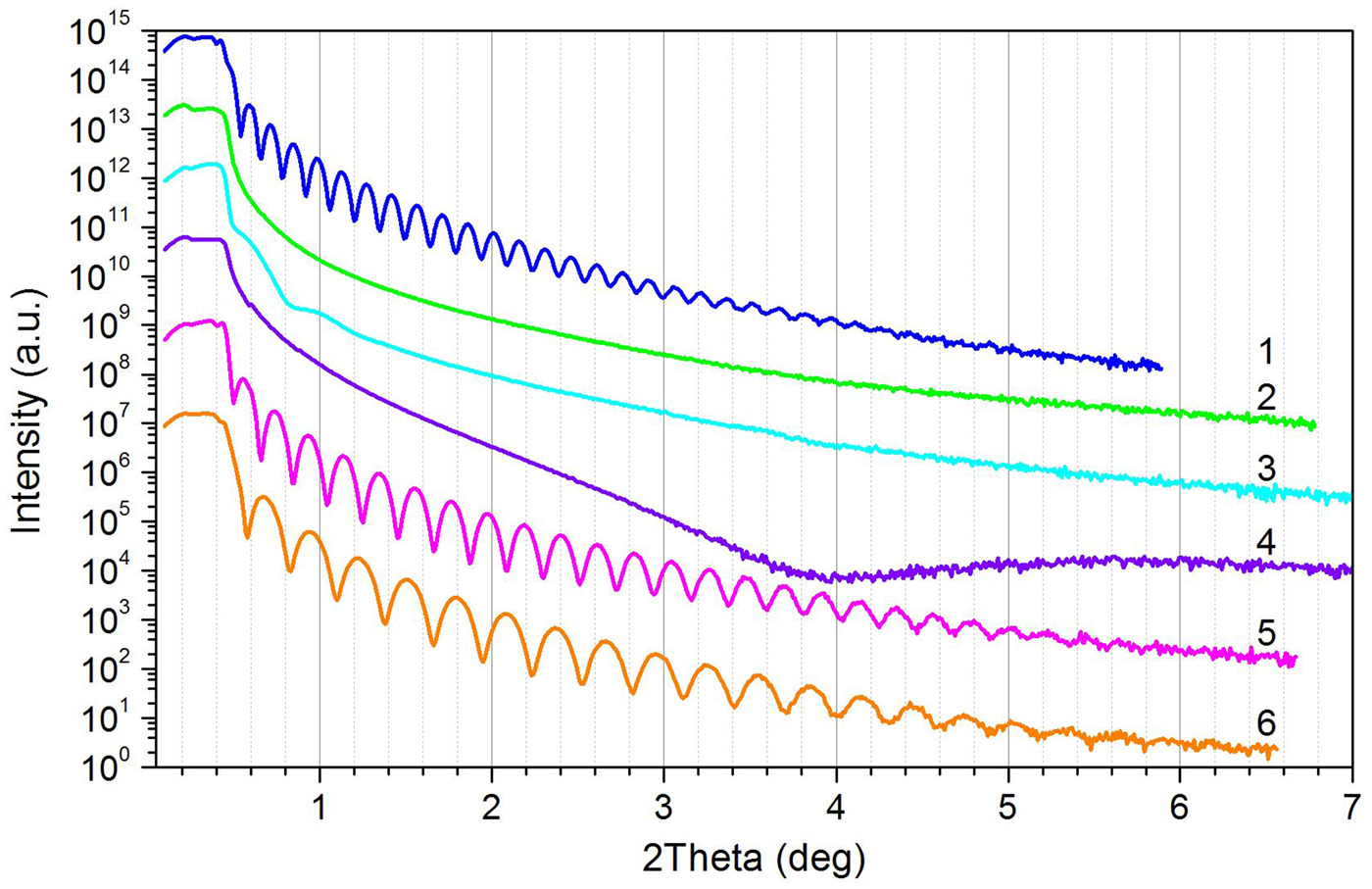
Figure 9. (Colour online) XRR patterns of random P(MMAm/XMAn/sfMA-H2F6o) with X = Pg, BP and variable m, n, and o. Variation of film preparation: 1 – H2F6-2(a), BP/o = 90 mol%; 2 – H2F6-2(b), BP/o = 80 mol%; 3 – H2F8-2(c), BP/o = 89 mol%; 4 – H2F6-3(a), Pg/o = 42 mol%; 5 – H2F6-3(b), Pg/o = 42 mol%; 6 – H2F6-3(c), Pg/o = 42 mol%. Film preparation with different solvents (PFO: (a); BFMB: (b), (c)), and annealing times (4 h: (a), (b); 48 h: (c)). (For further details see Table I).
It can be concluded that the generation and quality of layer structures in thin films of sf copolymers is a function of sf side chains as well as preparation conditions. PFO as a solvent for the sf polymers allowed preparing films with the best quality. The d-values of the layer structure generated by the sf side chains were smaller than in the bulk samples (compare bulk and film values in Table I). The reason, therefore, is mainly seen in the confinement conditions.
C. Structure of semiconductor films
P3HT films were also prepared by spin-coating on Si-wafer. The film thicknesses f were up to ~76 nm. The parameter of P3HT films (single layer) is documented in Table III. The ordering behavior of P3HT films has been reported widely in the literature (Chang et al., Reference Chang, Sun, Breiby, Nielsen, Sölling, Giles, McCulloch and Sirringhaus2004; Hugger et al., Reference Hugger, Thomann, Heinzel and Thurn-Albrecht2004; Ma et al., Reference Ma, Yang, Gong, Lee and Heeger2005; Colle et al., Reference Colle, Grosso, Ronzani and Zicovich-Wilson2011). The rigid polymer backbone of P3HT should support the layered head-to-head arrangement of the hexyl side chains in a similar manner as shown for the H2F8-sf side chains. Hexyl side chains in polymers with flexible backbones like in poly(methacrylate)s usually have only very weak structure formation (Beiner, Reference Beiner2001; Beiner et al., Reference Beiner, Kabisch, Reichl and Huth2002). P3HT clearly revealed d-spacings originating from two weakly interdigitating hexyl chains (Chen et al., Reference Chen, Wu and Rieke1995).
Table III. Results of film investigation by XRR: Double layer films of random P(MMAm/XMAn/sfMA-HxFyo) on top of a P3HTsubfilm.

n.m. – not measured; n.d. – not detectable; n.c. – not calculable.
*P3HT subfilms were prepared with solvent CHCl3, polymer concentration, and time of annealing at 130 °C in a vacuum. d P3HT correlates to the (100)P3HT reflection (in bulk).
**All top dielectric films were prepared with 1 wt.% solutions of copolymers in BFMB (but °: PFO), and annealed 4 h at 130 °C in a vacuum.
•Estimated f diel-values were based on the equation: f P3HT + f diel = f total; with f P3HT and f total– found in the double films XRR pattern.
Figure 10 shows the influence of the copolymer concentration in the solution for the preparation by spin-coating. A high film quality could be reached for all concentrations used. Basing on the knowledge of the crystalline structures of P3HT (Hugger et al., Reference Hugger, Thomann, Heinzel and Thurn-Albrecht2004; Wu et al., Reference Wu, Xin, Kim, Ren and Jenekhe2009; Colle et al., Reference Colle, Grosso, Ronzani and Zicovich-Wilson2011; Xiao et al., Reference Xiao, Zhang, Bryan, Jasensky, McNeil and Chen2015), the (100) reflection in the film should be visible at 2θ = 5.20 to 5.85° or in a small Δ2θ range around the reflection position in P3HT bulk material. In fact, the XRR curves were influenced by a weak intensity increase in this range. The measured Kiessig interferences were used to calculate the film thicknesses f as to be 95.3, 40.2, and 14.5 nm in dependence on the concentration. This relation is presented in Figure 11 together with a linear fit. Independent of the low number of data points, a linear function between film thickness and concentration seems to be likely. A minimum concentration from which a closed film can be expected is recognizable (to be at ~0.05 wt.% copolymer concentration).

Figure 10. (Colour online) XRR patterns of semiconductor P3HT: Dependence on P3HT concentration in the CHCl3 solution for thin film preparation (all samples were annealed). 1 – P3HT-1/0.50 wt.%; 2 – P3HT-2/0.25 wt.%; 3 – P3HT-3/0.10 wt.%. (For further details see Table III).
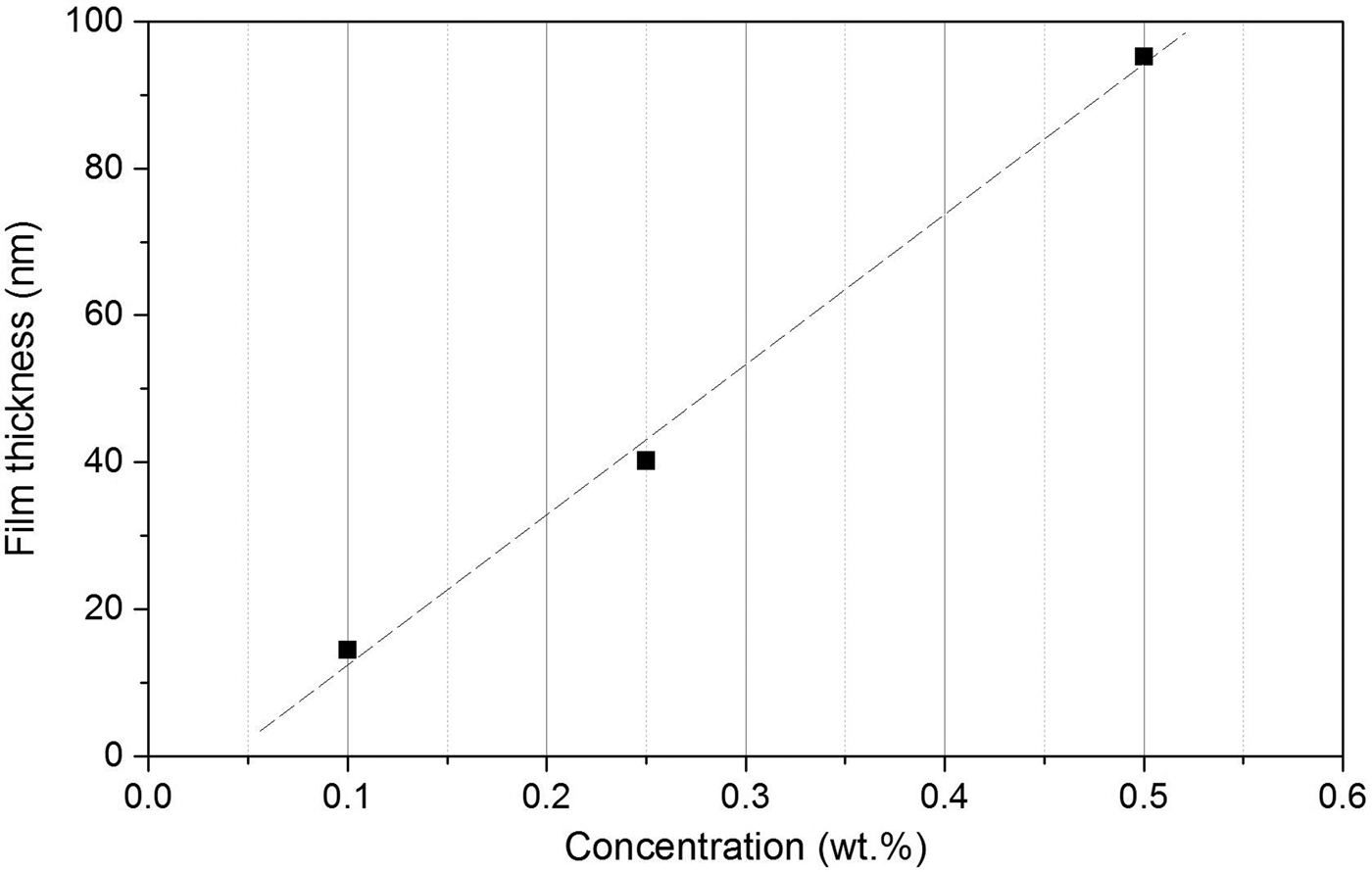
Figure 11. Thin film preparation of P3HT: Dependence of the film thickness on the P3HT concentration in the CHCl3 solution. Data taken from XRR curves in Figure 10. The dashed line represents the linear fit.
D. Structure of double layer films consisting of dielectric polymers and semiconductor
Double layer films of dielectric copolymers on top of a P3HT film were prepared under different conditions. It was examined whether or not the characterization with XRR is suitable to get structure information of such double layer systems and even indications about interactions at the interface between both layers, which is the most important area of the functionality in OFETs.
In Figure 12 the XRR patterns of double layers of different dielectric layers on top of a P3HT sublayer were compared. The upper four curves concerned dielectric polymers with sfMA-H2F8 and the lower three ones applied to those with sfMA-H2F6. Preparation parameters were the concentration of P3HT in the CHCl3 solution for spin-coating and the solvent of the solution for spin-coating the dielectric layer (i.e. BFMB and PFO). As figured out in the former discussion of dielectric single layers the knowledge of the crystalline structures of P3HT, in particular, the expected position of the (100) reflection (in bulk), was used to mark the small Δ2θ range around the reflection position. In fact, the XRR curves of the double layers were influenced by a weak intensity increase in this range, too. To observe any generation of layer structure caused by H2F8 side chains, the expected position of the related layer reflection (bulk value) was marked, too. Only in the double layer configuration with the thickest two single layers (sample H2F8-7@P3HT°) a weak intensity increase in this range of the XRR curves was visible.

Figure 12. (Colour online) XRR patterns of double layer films of different dielectric layers on top of a P3HTsubfilm. 1 – H2F8-10@P3HT, 2 – H2F8-12@P3HT; 3 – H2F8-12@P3HT°, 4 – H2F8-2@P3HT, 5 – H2F6-2@P3HT, 6 – H2F6-2@P3HT°, 7 – H2F6-3@P3HT (see Table III). All dielectric layers were prepared with 1 wt.% solutions of copolymers in BFBM and PFO (°), respectively, and were annealed. (For further details see Table III).
The measured Kiessig interferences (in simple appearance) were used to estimate the related source and film thicknesses. f was in the range of ~17 to ~43 nm (received for solution concentrations of 0.10 and 0.25 wt.%, respectively). The comparison with results received for the single layers of P3HT let assume that the detected XRR patterns were representative for P3HT layers only (the small variations should be caused by the preparation).
Two samples (on P3HT basis layers with f ~40 nm) were prepared using PFO as a solvent and showed a superposition of two different XRR curves, which could be evaluated separately to get two f-values (see Table III). It is obvious that the lower value related to the P3HT sublayer thickness f P3HT, but the larger one to the total film thickness f total. The so assigned P3HT film thicknesses were significantly higher (48.1 to 58.7 nm) compared to that of single layers using BFMB as solvent (see Figure 10 and Table III, above: 40.2 nm for P3HT-2). Using both experimentally found f-values, an estimation of the thickness of the dielectric layer was done. The values for f diel were in the range of calculated 63.5 and 73.5 nm for the dielectric layer with H2F6 and H2F8, respectively.
The parameters varied in the preparation of the double layer system influence the image of the XRR curves in a different manner. The selected samples measured give only a first impression about the diversity of implications. In summary, examinations of double layer films with XRR showed not reflectivity pattern generally, in which Kiessig interferences were generated with basic information about two representative layer thicknesses. Depending on layer roughnesses and related electron densities in the layers only one pattern was often found. An assignment to a concrete layer could be incorrect. To solve this deficit a modifying of experimentation: preparation and XRR measurement of the basic layer and – consecutively – the preparation of the top layer, and not till then a second XRR measurement of the double layer system.
For an optimization of preparation conditions more detailed investigations are necessary. In continuation, the interpretation of double layer system has to be verified by modulated experiments. And as a more theoretical help, the discussion will be supported by the whole pattern fits using appropriate models of the single films as well as of the double films prepared from these random copolymers.
IV. CONCLUSION
The structure formation of PMMA copolymers with self-organizing sf side chains and crosslinking units for use in organic electronics was examined in bulk and thin films. The generation of sf layers in bulk samples depended on both, length and concentration of side chains. While H10F10 side chains provided a strong self-assembly (with d sf-layer in the range of 5.0 nm), H2F8 forced an intermediate order (with d sf-layer in the range of 3.1 nm), whereas H2F6 side chains formed only a weakly ordered structure (with d sf-layer in the range of 2.9 nm). These sf layer thicknesses were smaller in thin films because of confinement effects of the film within substrate and air. In case of the interdigitated structure of H10F10, d sf-layer diminished by about 0.7 nm, that means, the sf layers were compressed, probably by stronger tilting of the side chains. The head-to-head structure of H2F8, in contrast, was only slightly compressed by about 0.2 nm. Shorter sf side chains resulted in higher quality thin films owing to the better solubility and less hydrophobic behavior. On the other hand, short sf side chains reduced the self-organization. Thus, an optimum between both has to be found.
Additionally, it has to be emphasized that the preparation conditions played a crucial role in the quality of the films and the XRR results. In particular, the use of perfluorooctane as solvent combined with thermal annealing at 130 °C for 4 hours improved the quality of the films significantly.
The same will hold for future applications in organic electronics. For suitable electric properties, the films are required to be defect-free. As the first step in this direction, double layers of the polymer semiconductor P3HT and the dielectric copolymers were examined by XRR. Under suitable conditions, the typical P3HT structure in the underlying layer was observable in the double layer, while the typical sf structure was only slightly indicated.
Acknowledgements
Financial support by Center for Advancing Electronics Dresden (CFAED) at Technische Universität Dresden, financed by Deutsche Forschungsgemeinschaft, is gratefully acknowledged (A. B.). Specials thanks also for the excellent collaboration within CFAED. The authors thank all colleagues from IPF participating in synthesis and characterization of the polymers (in particular, P. Treppe, SEC; K. Arnhold, DSC; R. Schulze, Ellipsometry). Archroma Germany GmbH, Burgkirchen, kindly provided the H2F6-sfMA monomer.


