I. INTRODUCTION
Radar absorbing materials (RAMs) are materials able to minimize the electromagnetic field scattered from them. They are usually realized as a coating whose electric and magnetic properties produce the absorption of an impinging radiation in a given frequency range. The direction of the incident wave being unknown, it is of paramount importance that absorption is granted for the widest possible range of incidence angles. RAMs have many possible applications, like shielding from electromagnetic interference, but the most common is the reduction of a target's radar cross section (RCS). The RCS of an aircraft or of a ship determines the detectability of the target itself: by covering the target with RAMs, the incident electromagnetic energy is absorbed and then the RCS is reduced.
The first and simplest absorber is the Salisbury screen [Reference Salisbury1, Reference Fante and McCormack2]: it consists of a single resistive sheet placed λ/4 in front of a perfectly conducting ground plane. The sheet impedance is purely real and equals that of free space. Such a structure is able to achieve a great absorption but only for a very narrow bandwidth and normal incidence. A large number of papers aim at obtaining better Salisbury screens, for example, for what concerns bandwidth [Reference Smith3], angular sensitivity [Reference Seman, Cahill and Fusco4], thickness [Reference Seman, Cahill and Fusco5], and frequency tunability [Reference Chambers6, Reference Smith7]. If the number of sheets is increased, the resulting structure is named Jaumann absorber [Reference Emerson8] and can achieve a wider band and a reduced angular sensitivity with respect to the Salisbury screen [Reference Munk, Munk and Pryor9].
Although the conventional Salisbury and Jaumann structures exploit uniform impedance sheets, which are purely real and frequency independent, several of the solutions proposed to improve the absorption performances and widen the bandwidth exploits sheets with complex, frequency-dependent impedance. This can be achieved by substituting the resistive sheets with a frequency-selective surface (FSS) comprising lossy elements [Reference Munk10]. This type of design leads to the so-called circuit analog absorbers (CAA). The elements forming the FSS can have any shape, but the best results are usually achieved using loop elements. The main issue in these solutions is the necessity of lumped resistive loads for the elements to obtain the required losses [Reference Munk, Munk and Pryor9]. These loads make the CAA technically difficult to manufacture and hence both highly costly and frail.
In this paper, an alternative design in which the resonant rings of the FSS are made of a high-loss homogeneous material, without lumped loads, is presented. The absorbing surface proposed is aimed at absorbing the incident waves in the 6–16 GHz band for the widest possible range of angles of incidence. Single- and double-layered FSS designs will be analyzed.
The material chosen here to realize the FSS rings is an isotropic sheet of multi-walled carbon nanotubes “CNT”, whose electrical properties have been recently assessed [Reference Wang, Zhou and Xin11]. This material not only presents high losses, but also a very high permittivity, allowing, as will be shown in the following, for a very limited angular sensitivity.
Actually, the relatively high losses and permittivity allows for substantial absorption from the CNT-based CAA without the need for the above-mentioned costly and frail lumped loads.
Indeed, a few examples of CNT-based absorbers do exist, mostly at optical frequencies [Reference Uchida, Martinez, Song, Yshigure and Yamashita12, Reference Kashiwagi, Yamashita, Yasu, Yaguchi, Goh and Set13] and quite few at microwaves [Reference Saib14]; actually previous works on carbon fibers, not nanotubes, are also present [Reference Neo and Varadan15]. In all these papers, CNT are exploited as uniform layers, whereas in this paper a periodic FSS is exploited.
The analysis of the CNT-based FSS is performed here by finite-element (FE) analysis over a single periodic cell. On the basis of these full-wave results, an equivalent admittance of the FSS sheet is obtained to be used in the transmission line model of the CAA. The design of the absorber is then performed over this simplified model and the final design is validated by a separate full-wave FE analysis.
The paper is organized as follows. Section II presents the FSS exploited for the absorber and the transmission line model which can be derived from it. Section III presents the design of the single- and multi-layered absorbers together with numerical results and validations. Finally, Section IV will draw some conclusions.
II. FSS MODEL
A Salisbury screen can be modeled, in a transmission line approach, as comprising a shortened transmission line loaded by a Z 0 impedance one quarter wavelength from the short. This model explains both why the Salisbury screen works and why it is narrow banded. The short circuit reverts to an open circuit at a distance equal to λ/4 and this zero admittance load is in shunt with the Z 0 load, which is hence unaltered and matched to the line. This holds only at the frequency where the distance is λ/4 and only for normal incidence. The arrangement of several resistive sheets simply augments the number of shunt loads on the line.
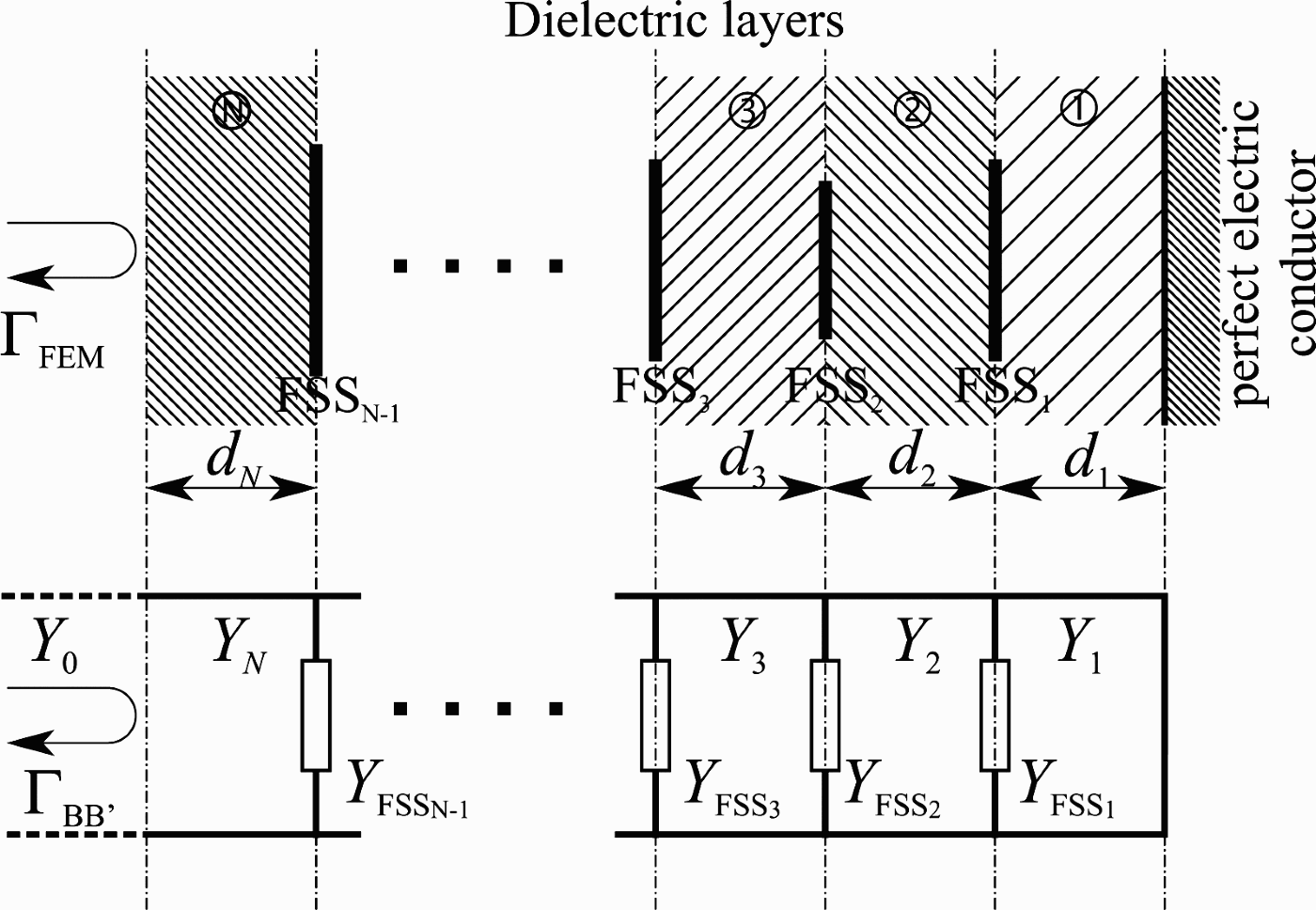
For an FSS screen the circuit interpretation as a shunt load still holds (Fig. 1). The key point is how to estimate the value of the shunt load. A possibility is that of performing a full-wave simulation of the FSS screen and recovering the value of the shunt load over a frequency band from the computed reflection coefficient, hence allowing the construction of a look-up table of possible load values for the synthesis of the absorber.

Fig. 1. Schematics of an FSS embedded in two dielectric layers (top) and equivalent transmission line circuit (bottom).
Among the various possible full-wave solutions for an FSS screen, the finite-element method (FEM) applied over a single periodic cell and with the enforcement of a suitable expansion in terms of Floquet modes is a well-established approach [Reference Pelosi, Coccioli and Selleri16, Reference Pelosi, Freni and Coccioli17]. If the periodicity of the FSS is half a wavelength or less, then only the zero-order Floquet mode propagates and all the higher harmonics are evanescent [Reference Pelosi, Coccioli and Selleri16], and hence the transmission line model can be applied and, by defining the reflection coefficient ΓFEM in terms of the ratio between the amplitude of the single propagating Floquet wave E 0(f) and the amplitude of the incident wave E (i)
the FSS admittance Y FSS can be easily computed. Indeed, the reflection in the line ΓBB′ coefficient transported at the FSS position is ΓAA′ = ΓBB′e j2k 2d 2, being k 2 the wave number in the transmission line which for normal incidence coincides with the wave number in the dielectric layer. The total admittance in AA′ is
but Y AA′ is the sum of the unknown Y FSS and of the short circuit transported by d 1 whose value is Y short = −jY 0cot (k 1d 1), and hence
where ΓBB′ = ΓFEM is also assumed.
III. ABSORBER DESIGN AND NUMERICAL RESULTS
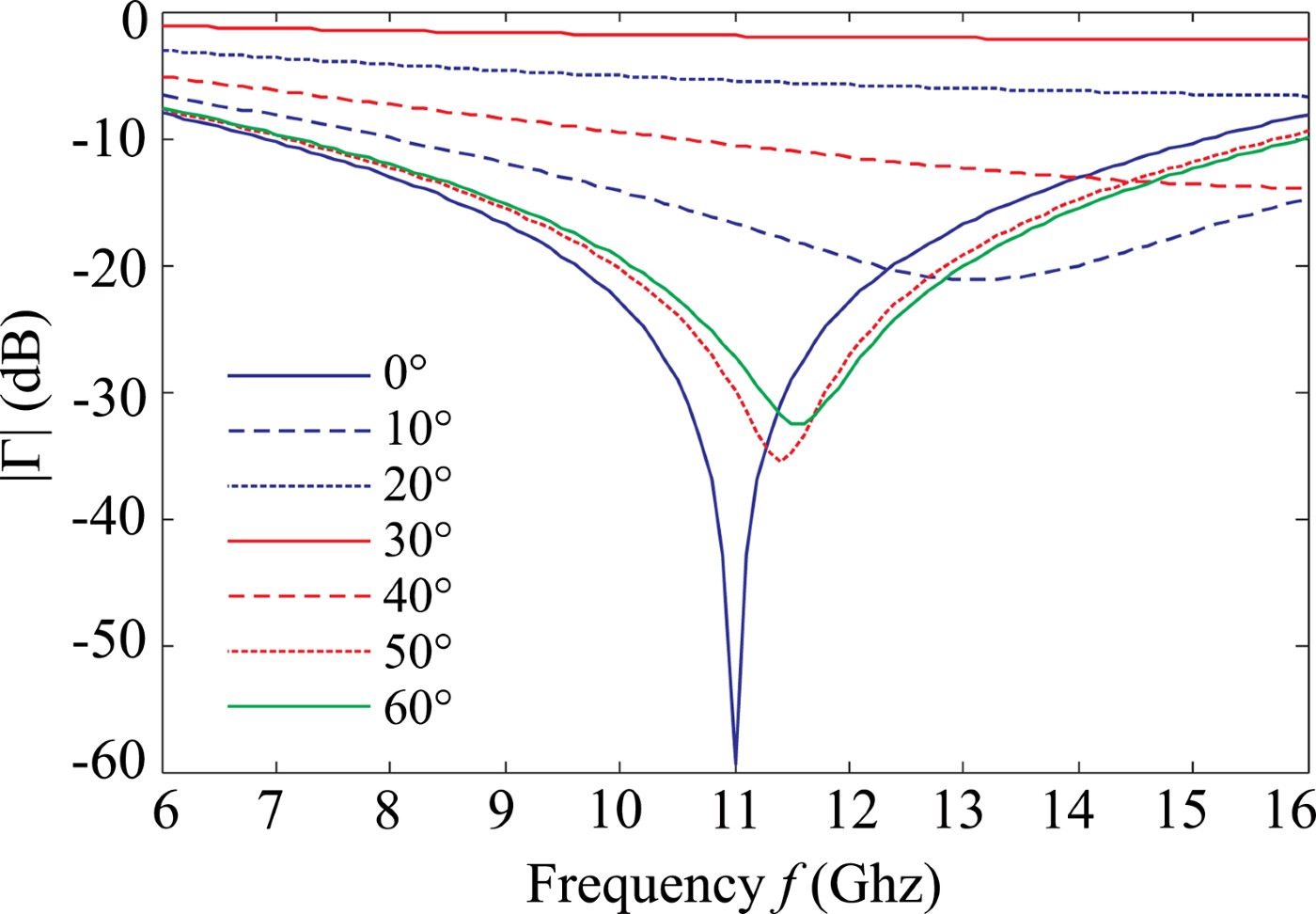
As already mentioned, the Salisbury screen provides good absorption but only on a very narrow bandwidth. Furthermore, as the angle of incidence varies, the absorbing performances worsen (Fig. 2).

Fig. 2. Salisbury screen performances as a function of the angle of incidence of the plane wave.
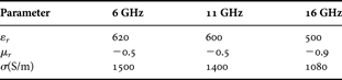
As a possible upgrade, a single-layered circuit analog absorber has then been analyzed: such structure is made of a single FSS layer of CN resonant rings. The geometry of the FSS is sketched in Fig. 3; rings have an inner radius r in = r 0 − Δr/2, and an outer radius r out = r 0 + Δr/2, r 0 such that 2πr 0 = λ0 with λ0 being the free space wavelength at the design central frequency f 0 and Δr = λ0/60. The thickness of the FSS rings is set to t = 88.9µm and rings are arranged in a square lattice characterized by periods d x = d y = λ0/2. The CNT material exploited is that is described in [Reference Wang, Zhou and Xin11] where its full electromagnetic characterization can be found. For the sake of completeness Table 1 reports these values at band extremes and at center band. The FSS is then embedded within two dielectric layers exhibiting ɛ1 = 1.5 and ɛ2 = 1, both being one-quarter-wavelength thick.

Fig. 3. Ring FSS geometry. At the center, in black, the periodic cell.
Table 1. CNT material parameters.
This design leads to much wider band absorption for normal incidence with respect to the Salisbury screen (Fig. 4). The frequency is fixed to f 0 = 11 GHz and the absorber behavior is analyzed as a function of the incidence angle for both parallel and perpendicular polarizations. The results in Fig. 5 show first of the presence of a periodic behavior with respect to the angle of incidence. This is due to the fact that the overall ring length is several wavelengths at 11 GHz, due to the very high permittivity of the material. Since the ring becomes an ellipse for the incident plane wave as the angle of incidence increases, its electrical length varies, generating noticeable differences in the currents, and hence in the losses, on the ring itself. This phenomenon differs on the basis of the incident wave polarization. Particularly for perpendicular polarization incidence (blue curve), the reflection coefficient is at least −7.5 dB on the entire angular range, whereas, for parallel polarization incidence (red curve), there are angles with nearly total power reflection. Performances hence need to be improved for what concerns the angular range of absorption. The design is hence shifted on an absorber with more than one layer of FSS.

Fig. 4. Carbon nanotube FSS absorber performances as a function of frequency.

Fig. 5. Carbon nanotube ring FSS absorber at 11 GHz as a function of the angle of incidence.
A multilayered structure can still be analyzed by the transmission line approach (Fig. 6). In our analysis, the various FSS are assumed to share the same periodicities d x and d y and the thickness of all the dielectric layers has been maintained equal to a quarter wavelength in the dielectric. The FSS being discontinuous surfaces, higher modes might arise, which, if the periodicity is half a wavelength or smaller, are in cutoff. Some coupling between FSS layers might arise due to cutoff modes whose decay is not strong. This coupling is neglected in a transmission line approach where only the dominant mode is modeled in the transmission line analogy.

Fig. 6. Multilayered FSS absorber (top) and its circuital equivalent (bottom).
Notwithstanding this approximation, a design carried out over an equivalent circuit is much faster than one based on a FE full-wave simulation, and hence the circuit analogy will be exploited and the full-wave analysis will be then applied to the obtained structure to have an a posteriori validation and verification of the performances.
The key issue here is determining the admittances realized by the CN ring FSS, for which an analytic formula is not available.
The approach exploited here is that of resorting to the look-up table of possible admittances realized as described in Section II for a wide range of inner and outer diameters and surrounding dielectrics. In particular, analyses have been done via full-wave FEM for ɛ1, ɛ2 ∈ [1,1.5,1.7,2] and ring radii r 0 ± 15% The analysis has been carried out for a discrete frequency set (6–16 GHz with 1 GHz step) and a discrete set of angle of incidence (0–60° with 5° step). A finer discretization would have led to a more complete look-up table but would have been too time consuming, and hence an interpolation of these values has been performed through an artificial neural network (ANN) trained to this aim and outputting the expected admittance of the FSS as a function of the variable geometrical and electrical parameters. ANNs are known to be exceptional approximators [Reference Hornik, Stinchombe and White18] and have been successfully used in electromagnetism in many different applications [Reference Selleri, Manetti and Pelosi19, Reference Manara, Nepa, Pelosi, Pinto and Selleri20].
Once the ANN is available, an optimization is carried out over the circuit analog problem, by employing a genetic algorithm (GA) over a suitable cost function. GA is a very well-established stochastic optimization method known to be efficient and able to avoid local minima very widely used in electromagnetics [Reference Haupt and Werner21–Reference Agastra23].
The key point of an optimization is the definition of a suitable cost function. In this paper, first of all a level L for the return loss is defined, to be used for the definition of the bandwidth of the absorber. For a given angle of incidence θn, the frequency range between the two points at |Γn| = −L dB is the pertinent bandwidth and is indicated with Δf n (Fig. 7). Once all angles of incidence θn, n = 1, … , N are computed, a single value Δf is computed as the intersection of all Δf n (Fig. 7). As the aim is to maximize the band, the cost function c is chosen proportional to the inverse of Δf. Of course, it can be a case where there are angles of incidence for which the reflection coefficient never falls below the −LdB threshold (Fig. 7, green curve). If this is the case for Ñ of the N angles of incidence under exam, a penalty factor ÑP, with P as a predefined positive constant, is added to the cost function.

Fig. 7. Sketch of possible reflection coefficients for the FSS absorber at different incidence angles and how they reflect on the cost function.
Furthermore, a merit factor is assigned to each curve whose center band is between 10 and 12 GHz, hence closer than 1 GHz to the desired value f 0 = 11 GHz. If there are Ñ angles of incidence for which the frequency behavior is centered in f 0, then a quantity Ñ Q is subtracted from the cost function, with Q a predefined positive constant.
In a single formula:
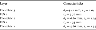
Several runs of the GA have been carried out, with the parameters reported in Table 2. Of the various designs attained in the following, it is reported as an example, the structure with three dielectric layers and two embedded FSS layers in Table 3, whose total thickness is about 17 mm.
Table 2. GA parameters.

Table 3. Optimized structure.

Figures 8 and 9 report, respectively, the frequency behavior at normal incidence of the synthesized structure and the variation of the reflection coefficient magnitude as a function of the incidence angle at 11 GHz for both parallel and perpendicular polarizations. These results are obtained by the full-wave FE analysis. In Fig. 9, the relevant dependence with incidence angle already noticed in the single-layered structure is still present, but the optimized structure guarantees at worst a reflection coefficient of −6.5 dB, with an average reflection coefficient of −15.4 dB for perpendicular polarization and −10.3 dB for parallel polarization. It is very important to stress that this rapidly oscillating behavior in the reflection coefficient is due to the very high permittivity and good conductivity of the CN-based material employed for the rings. Such behavior is highly desirable because it causes the average value of the reflection coefficient to stay quite low over a wide range of incident angles.

Fig. 8. Frequency behavior of the synthesized multilayered absorber.

Fig. 9. Variation of the reflection coefficient as a function of the angle of incidence for the synthesized multilayered absorber at 11 GHz.
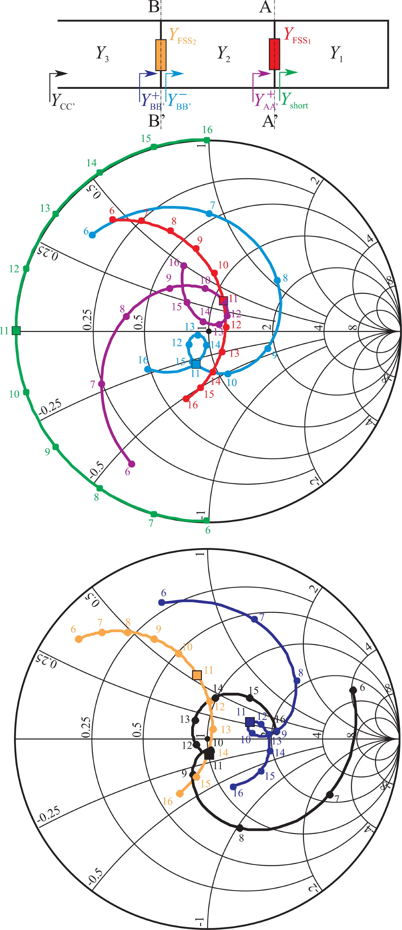
To gain a better insight of the characteristics of this absorber, its circuit analog behavior is presented over the Smith chart (Fig. 10).

Fig. 10. Circuit analog of the FSS (top) and frequency behavior, on the Smith chart, of the admittances in various points of the circuit.
Fig. 10 particularly shows, in different colors and over the 6–16 GHz band, the values of the normalized admittances along the circuit analog absorber: Y AA′+ = Y FSS 1 + Y short, Y BB′− is the transport of Y AA′+ along the Y 2 line, Y BB′+ = Y FSS 2 + Y BB′− and Y CC′ is the transport of Y BB′+ along the Y 3 line. All the admittances were normalized to the free space admittance η0 = ζ0−1 = (120π)−1 to reproduce them on the Smith chart.
By drawing the circles at |Γ| = 0.2 and |Γ| = 0.1, it is easy to derive (Fig. 11) the frequency band for which, at normal incidence, 96% of the impinging power is absorbed. Its value is 4.9 GHz (part of the curve within the |Γ| = 0.2 circle), while the band for which, at normal incidence, 99% of the impinging power is absorbed, can be evaluated equal to 3.4 GHz (part of the curve within the |Γ| = 0.1 circle). If the results of the full-wave simulation are plotted on the Smith chart too, the agreement with the circuit analog is very good (Fig. 11, red line) and bands appear a little larger: 5.3 and 3.6 GHz, respectively.

Fig. 11. Frequency behavior of the synthesized multilayer absorber at normal incidence (black line) and corresponding full-wave simulation (red line).
Finally, Fig. 12 reports the curves of the amplitude of the reflection coefficient as a function of frequency for a very fine discretization of possible angles of incidence in the [0°, 3°] range. Such a range was chosen, because it encompasses the first period of the pseudo-periodic variation of the reflection coefficient (Fig. 9).

Fig. 12. Variation of the reflection coefficient over the 6–16 GHz band at various incidence angles and perpendicular polarization.
The hatched area in Fig. 12 highlights that the CNT-based dual-layered FSS absorber guarantees at least a −10 dB value for |Γ| in a 9.05–14.35 GHz band for any incidence angle in [0°, 3°], and thanks to the periodicity due to the peculiar electrical characteristics of the CNT material, for any angle of incidence up to 60°.
IV. CONCLUSIONS
In this paper, the design of a CNT-based dual-layered FSS absorber has been carried out. The use of this novel material was essential in achieving good absorption over a wide angular range, thanks to its very high permittivity and good conductivity.
In the development of the design, a number of algorithms and procedures aimed at speeding up the procedure with respect to a conventional design based on full-wave FEM simulations have been developed. These algorithms are able to extend the project to an absorbing structure with any number of FSS layers, even if the increase in thickness might limit the applicability of the attained results over vehicles.
 Ugo F. D'Elia was born in Terracina, Italy on December 14, 1948. He received the Laurea (Doctor) degree in Applied Mathematics from the University “La Sapienza” of Rome, Italy 1972. He attended a specialization course by the Ministry of Posts and Telecommunications and served for military duty in the Italian Navy Ministry, Department of Operations Research. Main domains of Expertise are Electromagnetic and Numerical Modeling in the areas of: analysis and synthesis of all types of antennas, scattering and radar cross section prediction, simulation models of targets, antennas and propagation effects for missile radar system simulations. Numerical techniques, software, and advanced automatic measurement systems as the near-field antenna test ranges. He has been working, since 1974, at all the main antenna and radome projects for different missile and radar systems in MBDA Italy, formerly AMS (Alenia Marconi Systems) and SELENIA SpA.
 Giuseppe Pelosi was born in Pisa, Italy on December 25, 1952. He received the Laurea (Doctor) degree in physics (summa cum laude) from the University of Florence in 1976. He is currently Full Professor of Electromagnetic Fields and was a Visiting Scientist at McGill University, Montreal, Quebec (Canada) from 1993 to 1995 and Professor at the University of Nice-Sophie Antipolis (France) in 2001. G. Pelosi is mainly involved in research in the field of numerical and asymptotic techniques for electromagnetic engineering, with particular interest to antennas, circuits, microwave and millimeter-wave devices, and scattering problems. He is also very active in the divulgation of electromagnetic engineering and telecommunications history. He is the coauthor of over 300 scientific publications. He has been Guest Editor of several special issues of international journals and is also the coauthor of three books. G. Pelosi is a Fellow of the IEEE “for contributions to computational electromagnetics.”
 Stefano Selleri was born in Viareggio, Italy, on December 9, 1968. He received his Ph.D. in Computer Science and Telecommunications from the University of Florence in 1997 and is an Assistant Professor there since 1999. In 1992, he was a visiting scholar at the University of Michigan, Ann Arbor, MI; in 1994 at the McGill University, Montreal, Canada; in 1997 at the Laboratoire d'Electronique of the University of Nice – Sophia Antipolis. From February to July 1998 he was a Research Engineer at the Centre National d'Etudes Telecommunications (CNET) France Telecom. In July 2007, he was a visiting professor at the Universidad Politecnica de Madrid, Spain, and in 2007 and 2008 was a visiting Professor at the University of Saarland, Germany. In October 2008, he was a visiting Professor at the l'University of Nice – Sophia Antipolis, France.
 Ruggero Taddei was born in Firenze, Italy, on February 12th, 1984. He received the B.S. degree in Computer Science Engineering in 2008 and the M.S. degree in Telecommunications Engineering (summa cum laude) in 2010, both from University of Florence, Italy. His main research interests are electromagnetic field theory, frequency-selective surfaces, and arrays.