Introduction
Frequency-selective surfaces (FSSs) are thin periodic pattern designed to filter electromagnetic (EM) waves based on the frequency range of interest [Reference Munk1]. It might be a single, double, multi, or broadband [Reference Li and Shen2–Reference Chaharmir and Shaker6]. In this sense, FSS is a virtue of regular 2D periodic array designed over a substrate material, usually metallic, sometime dielectric [Reference Oraizi and Afsahi7, Reference Li and Behdad8]. These surfaces found their potential applications in the design of antenna sub-reflectors, artificial magnetic surfaces, high-impedance surfaces, side walls of microwave oven to prevent the EM field leakage, radomes, radar-absorbing structures, and modern metamaterials [Reference Shivnarayan and Jha9].
Though not explicitly mentioned in the name, FSSs also have properties which may vary with incidence angle and polarization as well. These are unavoidable consequences of the way in which conventional FSSs are constructed. Moreover, the applications of 2D FSSs are limited because of its narrowband and unstable response. A miniaturized FSS elements have been reported in the open literature for stable resonance performance [Reference Yang, Zhang, Li and Wu10, Reference Yan, Qu, Wang, Zhang, Zhang, Xia and Wang11]. Aforementioned, elements may disintegrate at higher power levels and loss their basic functioning [Reference Munk, Luebbers and Mentzer12, Reference Liu, Booske and Behdad13]. The periodic surfaces, used in microwave applications, are continuously exposed to high average powers. Hence, the lossy materials will develop heat and result in melt/burn of conducting patterns. Moreover, very high electric fields will develop in the patch or slot elements. It will induce arcing effect that makes the surface short-circuited and non-operational. Increasing the gap between unit cells and thickness of substrate is one of the solutions to this problem. However, only moderate improvement is possible with this approach [Reference Munk1]. It is well known that the high-power handling and bandwidth (BW) can be achieved using thick metal but it leads to a bulkier structure.
The aforementioned limitations of 2D FSS can be overcome by using multilayered or 3D FSS structures [Reference Lu, Liu and Huang14, Reference Lee and Hong15]; whereas, the structural complexity is improved. Moreover, weight of the structure increased. The increased weight and payload make them unsuitable for many real-time and aerospace applications. A concept of series vais has been used in SOI to reduce the cross talk [Reference Joardar16]. The substrate-integrated waveguide (SIW) technology has been introduced into FSS design for better performance (high Q-factor) by upholding the unit-cell properties when it is used as an infinite surface without altering its resonant characteristics [Reference Luo, Hong, Hao, Liu, Li, Chen, Zhou and Wu17]. It can also show a stable response w.r.t the angle of incidence [Reference Xu, Zong, Yang and Wu18, Reference Luo, Hong, Lai and Sun19]. Hence, it is believed that the FSS structures using SIW technology can overcome the limitations of both 2D (instability) and 3D (weight) FSS structures and work as 2.5D FSS structure. The EM performance of FSS elements has been improved and enhanced passband characteristics have been achieved by using SIW technology [Reference Qi, Gong, Zhang and Liu20, Reference Xi, Hong, Wu, Hong, Hao, Chen, Zhou and Zhou21]. Recently, an FSS with narrow band configurable polarization rotator with minimal insertion loss is demonstrated using the concept of SIW technology [Reference Mollaei22].
As of now, the researchers developed slot-type FSS based on SIW technology to improve its performance. When dealing with the patch-type FSS, creating vias around the unit element leads to the formation of another resonance which disturbs the original performance of unit cell. To overcome this limitation, a novel design is reported in this paper. The design procedure of proposed structure is explained in further section. So far, the complex numerical techniques such as finite difference time domain (FDTD) method, MoM/Bi-RME, and commercial simulation software packages have been used to analyze this type of structures, which may take more computation time to execute the problem [Reference Luo, Hong, Hao, Liu, Li, Chen, Zhou and Wu17, Reference Winkler, Hong, Bozzi and Wu23].
In this paper, a single square loop (SSL), a loop type, and a Jerusalem cross (JC), a center-connected type elements, have been chosen to prove the enhancement in their stopband and stable response using SIW technology. The structures are designed to resonate at 10 GHz by considering its tremendous applications in civil, military radars, air traffic control and defense tracking. An equivalent circuit (EC) model is derived for both chosen elements to analyze the structural response. The described ECM technique can closely predict the transmission and reflection characteristics at a normal and oblique angle of incidence for both parallel (TE) and perpendicular (TM) polarizations. Further, the proposed technique can eliminate undesirable coupling between adjacent FSS elements. Moreover, the designed FSS will act as a virtually thick screen, which may be useful for high-power handling. Finally, the results obtained using the derived EC model is verified with the help of full-wave simulation (FDTD-based commercial simulation package CST Microwave Studio (CST MWS)) and measured results.
EM design of FSS–SIW element
Generally, conventional FSS array is printed on one side of a dielectric substrate. In this work, a 2.5D FSS is implemented using the SIW concept. To facilitate, two identical FSS elements are printed on top and bottom side of a thin dielectric substrate (thickness, t ≤ λ eff/4 where  $\lambda _{eff} = \lambda _0/\sqrt {\varepsilon _r} $) and connected by means of thin metallic vias (series of thin cylinders) results in incorporation of SIW concept in FSS design. In this study, two kinds of FSS elements viz. a SSL and a JC which are examples of loop-type and center-connected FSS elements, respectively, have been chosen for further investigations. Figures 1(a) and 1(b) illustrate the unit-cell models of improved FSS structure based on SIW technology. In loop-type FSS, the proposed concept will resemble the Faraday cage. The FSS elements printed on both sides of dielectric substrate act as a parallel combination of L, C equivalent tank circuit. Metallic vias will act as an inductive element (Lvia) connected in series and small intrinsic capacitive effects (Cvia) due to the dielectric spacer is connected in parallel to Lvia. The modified equation of ε eff [Reference Ferreira, Caldeirinha, Cuiñas and Fernandes24] has been used in the EC model to estimate the scattering performance of the structures with low estimation error. It is worth to mention that in [Reference Ferreira, Caldeirinha, Cuiñas and Fernandes24] authors presented the rigorous analysis to optimize the EC models. However, this work is different from the conventional FSS elements. The proposed FSS elements consist of two layers strongly connected through metallic vias. The structure has a very stable performance and higher BW compared with the FSS in its established form. In addition, it presented the EC models to analyze the structure response. The via has been modeled as an inductance, and the gap between two FSS elements is modeled as mutual capacitance. The transmission line approach is used to evaluate the total impedance and scattering characteristics of the structure.

Fig. 1. Geometry of proposed 2.5D FSS unit cell based on SIW (substrate is hidden to show the structure clearly): (a) square loop, (b) Jerusalem cross (substrate has been hidden to show the structure clearly).
Square loop
The pictures presented in Figs 2(a) and 2(b) show a unit-cell geometry and its corresponding EC model of a conventional SSL FSS, respectively. The same element is considered for showing the SIW technology with interconnected metallic vias from top FSS layer to bottom FSS layer and its improved EC model shown in Figs 2(c) and 2(d). The final design dimensions of SSL FSS are: periodicity p = 9.25 mm which corresponds to ≈0.308λ 0 (λ 0 be the free space wavelength at 10 GHz), d = 7.5 mm, s = 0.6 mm. The gap between two adjacent unit cells is g, which is equal to (p–d). The diameter and center to center spacing of metallic vias are D_via = 0.4 mm and K_via = 0.635 mm, respectively. The conducting metal patches of FSS are made of copper coating with a metal thickness of microns. The L and C values of square loop have been computed by its EC model given in equation (1)–(5). EC model offers an easy and quick method in FSS analysis. It serves as a good alternative to EM simulation.
 $${\rm For\ TE},X_L = \omega L = \left( {\displaystyle{{d\cos \theta} \over p}} \right) \cdot F\lpar {\,p,2s,\lambda, \theta} \rpar ,$$
 $$B_C = \omega C = 4 \cdot \varepsilon _{eff} \cdot \left( {\displaystyle{{d\sec \theta} \over p}} \right) \cdot F\lpar {\,p,g,\lambda, \theta} \rpar ,$$
 $${\rm For\ TE},X_L = \omega L = \left( {\displaystyle{{d\sec \phi} \over p}} \right) \cdot F\lpar {\,p,2s,\lambda, \phi} \rpar ,$$
 $$B_C = \omega C = 4 \cdot \varepsilon _{eff} \cdot \left( {\displaystyle{{d\cos \phi} \over p}} \right) \cdot F\lpar {\,p,g,\lambda, \phi} \rpar ,$$
where ε eff is the effective dielectric constant. F( · ) is a function of design variables p, s, d, g and incident angle (θ, ϕ) depends on polarization which is given as:
 $$F(\,p,w,\lambda, \theta ) = \displaystyle{\,p \over \lambda} \left[ {\ln \left( {\csc \displaystyle{{\pi w} \over {2p}}} \right) + G\lpar {\,p,w,\lambda, \theta} \rpar } \right].$$
In above equations, G( · ) is the correction term given in [Reference Ferreira, Caldeirinha, Cuiñas and Fernandes24]. In Fig. 2(d), Za and Z b correspond to impedances offered by the top and bottom FSS layers (Z a = Z b = Z FSS), respectively, which are computed by L and C. Z vias is the impedance offered by the inductive posts connected to both FSS elements which is explained in the next section.

Fig. 2. Square loop FSS unit-cell geometry: (a) SSL, (b) equivalent circuit model, (c) 2.5D SSL–SIW, (d) improved equivalent circuit model.
Jerusalem cross
JC is one of the classical elements used in FSS analysis [Reference Langley and Drinkwater25]. Hence, it is chosen as an example of center-connected FSS element. Figures 3(a) and (b) shows a unit-cell geometry and its corresponding EC model, respectively; whereas, Figs 3(c) and 3(d) show the proposed structure and its EC model successively. The final design dimensions of JC FSS are: p = 9.25 mm which corresponds to period of element. Arm's length of JC is d = 2.3 mm and the width of JC cross and arm is w = t = 0.65 mm. The gap between two adjacent unit cells is g, which is equal to (p–d). The proposed structure is analyzed on R04003C substrate with ε r = 3.38 having a thickness h = 0.81 mm. The L and C of JC element is computed by Equations (6)–(9) [Reference Langley and Drinkwater25].
 $${\rm For\ TE}:X_L = \omega L = \left( {\displaystyle{{\,p\cos \theta} \over d}} \right)F(\,p,w,\lambda, \theta ),$$
 $$B_C = \omega C = 4 \cdot \varepsilon _{eff} \cdot F(\,p,g,\lambda, \theta ),$$
 $${\rm For\ TM}:X_L = \omega L = \left( {\displaystyle{{\,p\sec \phi} \over d}} \right)F(\,p,w,\lambda, \phi ),$$
 $$B_C = \omega C = 4 \cdot \varepsilon _{eff} \cdot F(\,p,g,\lambda, \phi ),$$
where F( · ) and G( · ) are function of design variables and correction term, respectively, as described in the previous section. The dielectric effects of substrate material have been considered for better estimation of the resonance characteristics. In the proposed EC model, the classical ε eff has been replaced with the improved empirical model. Equation (10) gives better approximation than ε eff when used for the computation of capacitance.
 $$\eqalign{\varepsilon _{corr} = &\displaystyle{{\varepsilon _r + 1} \over 2}-\displaystyle{{\varepsilon _r-1} \over 2}\cdot e^{(-13h/p)} \cr & -\left( {\displaystyle{{100s^2} \over d}-2g + 10h} \right){\rm m}^{-{\rm 1}}.} $$
The normalized impedance w.r.t free space impedance (Z FSS = Z a = Z b) offered by conventional SSL and JC FSS elements is computed by the EC models based on the lumped elements induced by the structure [Reference Ferreira, Caldeirinha, Cuiñas and Fernandes24, Reference Langley and Drinkwater25]:
 $$Z_{FSS} = j\left( {\displaystyle{{X_g} \over {1 + jX_g}}} \right),$$
where X g is the reactance offered by the grid elements which is expressed as:
 $$X_g = \left( {X_L - \displaystyle{1 \over {B_C}}} \right),$$
where L and C are the inductance and capacitance offered by the patch elements on the dielectric substrate, respectively.

Fig. 3. Jerusalem cross FSS unit-cell geometry: (a) JC FSS, (b) equivalent circuit model, (c) 2.5 D JC–SIW, (d) improved equivalent circuit model.
Two FSS layers as a top and bottom surfaces and connected through metallic vias will act as a π network. The normalized impedance of total structure is Z FSS−SIW, viewing from input port with open-circuited output port of a π network given in equation (13)
 $$Z_{FSS\_SIW} = \displaystyle{{Z_a \cdot (Z_{via} + Z_b)} \over {Z_a + Z_b + Z_{via}}},$$
where Z via is the impedance offered by the metallic via and dielectric spacer whose EC is given below. The L via and C via are connected in parallel whose impedance is given as:
 $$Z_{via} = j\left( {\displaystyle{{\omega L_{via}} \over n} - \displaystyle{1 \over {\omega C_{via}}}} \right),$$
where n represents the number of vias in one unit cell. Thin metallic vias will act as a wire inductor and inductance offered by the wire (L via) is computed from equation (14) [Reference Grover26].
 $$L_{via} = 2L\left\{ {\ln \left[ {\left( {\displaystyle{{1 + \sqrt {1 + S^2}} \over S}} \right)} \right] - \sqrt {1 + R^2} + \displaystyle{\mu \over 4} + S} \right\}nH{\rm,} $$
where  $S = D\_via/2L,R = \sqrt {1 + S^2} $, D_via and L are the diameter and length of the metallic vias. The length of metal vias is same as that of thickness of the dielectric substrate (L = h). The numerical value of via inductance computed with equation (14) is L via = 0.724 mH and capacitance value is C via = 2.39 pF which is computed using the relation ε A/h, where h is the spacing between two metallic plates (height of the substrate) and A is the plate area. The initial values of D_via, K_via, and design parameters of FSS are computed at the centre frequency of 10 GHz. The necessary design rules are considered to design the metallic vias [Reference Deslandes and Wu27, Reference Krushna Kanth and Raghavan28]. The described EC model is valid for all element shapes. Here, the metallic vias can suppress the propagation of EM interference through the gap between the two parallel conducting FSS layers and SIW vias. The relationship between D_via and K_via can be satisfied to eliminate inter-elemental effects as found in equation (15) [Reference Deslandes and Wu27].
 $$K\_via \gt D\_via,$$
 $$(D\_via/K\_via) \gt 0.5,$$
 $$0.25 \lt \displaystyle{{K\_via} \over {\lambda _c}} \lt 0.05.$$
The condition (15a) states that the spacing between metallic vias should be larger than the diameter of the via to facilitate the physical realization. The condition (15b) is required to neglect the leakage through SIW vias. The number of vias should not exceed 20 per wavelength as stated in (15c). It is worth to mention that diameter of vias should not exceed the width of FSS element.
To show the effectiveness of derived formulas, the real and imaginary parts of the normalized impedances w.r.t maximum value, of both SSL and JC FSS elements in conventional form and using SIW technology, are shown in Fig. 4. It can be observed that the impedance response of the structure with SIW technology is improved significantly. Hence, the better impedance matching is possible in wide frequency region, And thus results in improving the BW. The resonance occurs when the inductive impedance is equal to capacitive impedance of the structure, i.e. real(Z) = imag(Z) = 0 of the circuit, which shown in Fig. 4.

Fig. 4. Real and imaginary part of normalized impedance of SSL and JC in conventional form and proposed 2.5D base on SIW technology on R4003C substrate with thickness h = 0.81 mm.
Finally, the corresponding voltage reflection coefficient of proposed FSS element with SIW technology “Γ” is expressed as:
 $$\Gamma = \displaystyle{{Z_{FSS\_SIW} - 1} \over {Z_{FSS\_SIW} + 1}},$$
where Z FSS−SIW is the normalized impedance of the structure. The power transmitted due to grid array |T|2is:
 $$\vert {\rm T} \vert ^2 = 1 - \vert \Gamma \vert ^2.$$
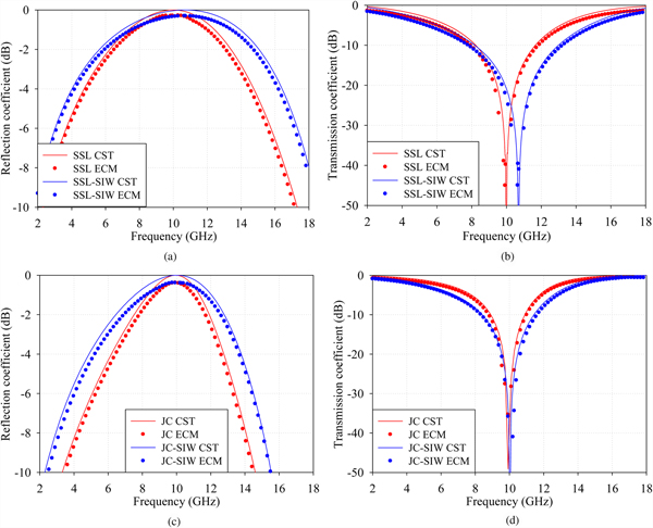
To show the efficacy of proposed EC mode for FSS with SIW technology, the results obtained with EC model are compared with an FDTD-based commercial full-wave simulation tool CST MWS. The unique feature of unit-cell boundary conditions with Floquet mode excitation is used to simulate the behavior of infinite FSS array. The results shown in Figs 5(a)–5(d) exhibit a good approximation between the analyzed FSS and FSS–SIW FSS elements using circuit model (ECM) and full-wave simulation. The structures are analyzed at X-band, all below figures are plotted on the scale from 4 to 16 GHz to observe the existence of higher order resonances. The reflection response shown in Figs 5(a) and 5(c) clearly shows the increment in their BW; whereas, the transmission parameters are presented in Figs 5(b) and 5(d), the −10 dB BW of the proposed FSS elements using SIW is improved significantly. The BW can further improve with proper tuning of the design parameters which is discussed in Section 3 of this paper. The EC method can give a knowledge of parametric effects such as dimensions of elements and dielectric parameters of substrate materials used in the design. Though, it is a powerful method to analyze the response of FSS structures with better accuracy and less CPU computation time (fraction of seconds); whereas, the simulation tools may take few minutes to hours depending on the structural complexity.

Fig. 5. EM-performance of FSS–SIW technology: (a) reflection coefficient comparison of SSL FSS and SSL–SIW FSS, (b) transmission coefficient comparison of SSL FSS and SSL–SIW FSS, (c) reflection coefficient comparison of JC FSS and JC–SIW FSS, (d) transmission coefficient comparison of JC FSS and JC–SIW FSS (bubbles show the response of FSS element with ECM and solid line shows the response with CST MWS).
The structures are analyzed from 2 to 18 GHz to observe the existence of unwanted resonances. From the transmission curves presented in Fig. 5, the −10 dB fractional BW of the proposed FSS elements using SIW is improved in SSL from 3.44 to 4.75 GHz and in JC FSS from 1.9 to 3.17 GHz in X-band region, as compared with their conventional shape, respectively. In case of JC SIW element, fractional BW obtained using EC model is 4.3 GHz (8–12.3 GHz) which is 1.3 GHz more compared with its conventional form (8.6–11.6 GHz). While the simulation results show 3.17 GHz (8.4–11.57 GHz) BW, whereas in the conventional form it is only 1.17 GHz (8.9–10.9). Accordingly, the relative error of BW for EC model w.r.t full-wave simulation is 35%. The resonant frequency is observed at 10.01 GHz using EC model and at 10.10 GHz by using simulation. Hence, root-square-mean-error of resonant frequency is only 0.89%. However, it is worth to remind that the EC model can help to estimate the initial response of the structure. Even though it is a powerful method to analyze the response of FSS structures with better accuracy and less CPU computation time, the simulation tools may take few minutes to hours depending on the structural complexity. Once the initial parameters have identified, the final design can be obtained using full-wave simulations.
Apart from the conventional FSS, the proposed structures show a very stable response at different angle of incidence. It has been observed in conventional FSS that the resonance frequency shifts toward lower frequency regime (left side) as the angle of incidence rise from 0o to 70o as shown in Tables 1 and 2 for SSL and JC FSS, respectively. The transmission and reflection characteristics of aforementioned FSS–SIW structures (loop and cross elements) at wide incident angles have been studied and presented in Figs 6(a)–(d), respectively. Very stable resonance characteristics for both TE and TM polarizations were observed at different angles of incidence. The frequency response of proposed SSL and JC elements using SIW over the conventional form is shown in Tables 1 and 2, respectively.

Fig. 6. Transmission and reflection coefficient of proposed FSS design at different angle of incidence: (a) SSL at TE polarization, (b) SSL at TM polarization, (c) JC at TE polarization, (d) JC at TM polarization.
Table 1. Effect of incident angle on the resonance performance of SSL

Table 2. Effect of incident angle on the resonance performance of JC

EM design of FSS–SIW element
The FSS, owing to the presence of SIW metallic vias in structure, results in an increase of BW and stable response w.r.t polarization at a different angle of incidence is achieved. The addition of SIW vias improves the EM performance. The vias used here will develop virtually thick FSS screens without altering its resonance performance.
However, there can exist limitations on structural dimensions of FSS elements and metallic vias, which can alter the required EM performance. The effects of structural dimensions of conventional FSS elements have been extensively reported in the earlier literature. In the proposed structure, the effect of substrate height, dielectric constant, and SIW vias are the main parameters needed to be considered to study the resonance performance. Moreover, in conventional form, the height of substrate and dielectric constant have contributed negligible effect. Whereas, in presented form, the dielectric spacer has been placed in between two FSS layers which act as a parallel plate capacitor (C = ε0εr/A, where A is directly related to the height of the substrate h). The capacitance will act in parallel to the inductive impedance induced by the metallic vias that can change the expected performance. The study helps to understand the behavior of FSS element with design parameters.
Effect of dielectric substrate
The dielectric substrate is used for physical support to FSS element. It is not only providing the physical support, but also a crucial parameter in the design of FSS. This substrate can have a profound effect on EM-performance of the structure [Reference Munk1]. The influence of the substrate parameters such as dielectric constant and thickness has been studied here.
Dielectric constant
Dielectric constant is an important parameter in the design of FSS. In general two things may happen when a dielectric substrate is loaded to the FSS: one, the resonant frequency (f 0) changes, also changes the BW for a different angle of incidence. Second, the periodic structure gets infinite support with relative dielectric constant (ε r). Since the structure has dielectric substrate in the center of two FSS layers, the resonant frequency shifts leftwards with a factor of  $f_0/\sqrt {(\varepsilon _r + 1)/2.} $ The variations in transmission coefficient as changing with dielectric constant are shown in Figs 7(a) and 7(b). From the observations made on the structures, it is found that different from its conventional form as ε r increases, increases the capacitive impedance of the structures makes the improving and BW.

Fig. 7. Influence of dielectric substrate parameters on the transmission response: (a) effect of εr on SSL FSS–SIW, (b) effect of εr on JC FSS–SIW, (c) Effect of h on SSL FSS–SIW, (d) Effect of h on JC FSS–SIW.
Thickness of dielectric substrate
Figures 7(c) and 7(d) show the variations in f 0 as the substrate thickness (h) increases. In established form, the substrate thickness have a negligible effect on the resonant and BW response of the structure. Different from conventional form, using SIW technology, the resonant curves shift toward the lower frequency regime. Hence, the substrate thickness of SIW has a primary effect on f 0 and BW whose effects cannot be ignored. Further increase in thickness, the proposed structure exhibits spectacular performance which cannot be found in the established form of FSS. The performance comparison of proposed FSS over conventional form at h = 8.0 mm is shown in Fig. 8. As thickness of the substrate approaches λ/4, the EM wane perturbations inside the structure lead to the occurrence of second higher order resonance, hence results in two strong stop bands at 9.26 and 15.86 GHz, respectively, with a very good passband in between them. In Fig. 8, the response of the proposed structure at the thickness of 8.0 mm (which is also equal to the height of the SIW vias) with different cell sizes has been presented. The substrate height is almost equal to λ/4 (quarter wavelength). The perturbation phenomena occur between the two metallic layers separated by the dielectric spacer. This effect results in the generation of second-order mode at higher frequency. As shown in Fig. 8(a), a higher order resonance can be seen at nearly 16 GHz on its transmission response. Consequently, there are two stopbands found at 9.0 and 16 GHz, respectively. Then there exists a strong pass band in between two stopbands from 9.8 to 12.3 GHz with fractional BW of 22.6% with better than 90% transmission efficiency. The corresponding reflection coefficient of the structure is shown in Fig. 8(b).

Fig. 8. Frequency response of proposed element at h = 8 mm at different cell size: (a) transmission, (b) reflection.
The extensive parametric study of proposed FSS proves the feasibilities of designing wideband FSS structures with stable resonance performance. It is well known that FSS is used as an infinite surface, where the weight of FSS plays an important role in practical applications. The proposed FSS has an advantage of lightweight because of the SIW cavities. Also, the size and thickness of the structure are 0.308λ 0 and 0.027λ 0, respectively, which is compact and ultrathin design suitable for real-time application without any further optimization. Moreover, it is also possible to realize 3D FSS elements with reduced weights using SIW cavity technology, which might be an interesting topic in future research.
Table 3 shows the comparison of literature results with the proposed structure. From the comparison, it is clear that the proposed 2.5D FSS exhibits improved BW at ultrathin thickness. Furthermore, the frequency response of the structure is very stable upto 60° compared with existing results.
Table 3. Comparison of existing results with proposed structure

Metallic vias
The metallic vias is the important design parameter of the proposed structure. The variations in the vias such as height, spacing, and diameter may affect the performance of FSS. For instance, the variation in the height of metallic vias in conventional form and proposed form is shown in Tables 4 and 5 for SSL and JC, respectively. Moreover, a better insight of vias (directly rated to height of substrate) has been presented in Fig. 8. For deep observation, the effect of vias such as spacing and diameter has been reported in the following sub-sections.
Table 4. Parametric effect on the resonance performance of SSL

Table 5. Parametric effect on the resonance performance of JC

Spacing between vias
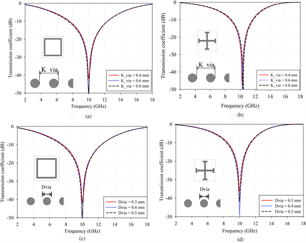
The metallic via spacing should satisfy the conditions given in Equation (15) to avoid the EM leakage through it. Based on the given conditions, the value of K_vas has been determined as 0.635 mm. The same value has been used in the entire analysis of both presented structures. For better understanding, to estimate the dependency of vias spacing on frequency response, a parametric study has been conducted on different design values of K_via at 0.4, 0.6, and 0.8 mm. Figures 9(a) and 9(b) show the transmission response of the proposed square loop and JC elements at different via spacing. It has been observed that the effect of via spacing within the considered limit is negligible.

Fig. 9. Influence of metallic SIW vias parameters on the performance of transmission coefficient: via spacing on (a) SSL FSS–SIW, (b) JC FSS–SIW element. Via diameter on (c) SSL FSS–SIW, (d) JC FSS–SIW element.
Diameter of vias
The effect of connecting metallic vias is studied in this section. From Figs 9(c) and 9(d), it is clear that the effect of vias diameter on the performance of FSS is insignificant. The transmission curves are almost same as increasing the diameter from 0.3 to 0.5 mm. After all, care should be taken while choosing the diameter of vias, i.e. it should not exceed the width of conducting element. The inductance offered by the metallic post mainly depends on the length of via then in its diameter. The purpose of vias is to interconnect the two FSS elements placed on either side of the substrate. Hence, the diameter should not cross the limits of FSS element width which may lead to develop the higher order modes.
Fabrication and experimental verification
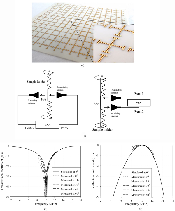
To prove the efficacy of analyzed results using EC method and full-wave simulation package, the proposed JC element with SIW vias structure has been fabricated using printed circuit board technology. A total of 16 × 14 cells are fabricated on 160 mm × 140 mm R04003C substrate with ε r = 3.38 having a thickness of h = 0.81 mm. The conductive periodic JC FSS array has been printed on either side of the substrate material. Then, the vias are made by drilling the holes with a diameter of 0.4 mm from the top layer to the bottom layer through the substrate and then coated with a thin copper material (0.035 mm) which can enable a metallic contact between the two layers. The fabricated prototype is shown in Fig. 10(a). In this setup, a pair of standard gain horn antennas (8.2–12.4 GHz) is connected to port-1 (transmitter) and port-2 (receiver) of ZVA 24 network analyzer (100 MHz–24 GHz) from Rhode and Schwartz. The structure is kept at the center of a pyramidal absorber to suppress the edge effects of the sample as shown in Fig. 10(b). Finally, the transmission and reflection curves of both simulated and measured values are compared at normal 60o incidence angle as shown in Figs 10(c) and 10(d), respectively. It can be seen that the measurement results are good in agreement with the analyzed results.

Fig. 10. Fabrication and experimental verification: (a) photograph of the fabricated prototype 16 × 14 array (inset shows the unit cell), (b) FSS measurement setup for transmission (left) and reflection (left) coefficient, (c) comparison of measured and simulated results transmission coefficient, (d) comparison of measured and simulated results reflection coefficient.
Conclusion
An approach to improve the BW and angularly stable 2.5D FSSs using SIW technology is presented. Two basic 2.5D FSS elements viz. square loop (loop type) and JC (center-connected type) have been investigated to prove the enhancement in their BW using SIW technology using ECM for initial estimation, further the final structure is obtained with the help of full-wave simulations using CST MWS. The parametric effects on the transmission response of the structures have been studied and compared with that of conventional form. The results prove the improvement in BW and angular stability of the proposed structure. Moreover, the structure is more suitable for real-time applications because of its ultrathin thickness (0.027λ 0). Finally, the measured results of the fabricated prototype prove the advantages of proposed structural topology.
Further studies on the proposed structures can serve the stable resonance. Also, prove as an alternative to 2-D and 3-D FSS structures with better EM performance characteristics for aerospace applications with reduced payloads and EMI shielding.
Author ORCIDs
Krushna Kanth Varikuntla 0000-0002-7429-8386.
Acknowledgement
Authors would like to thank Dr. D. C. Pande, Eminent Scientist, DRDO-LRDE, and Dr. Shivnarayan, CSIR-NAL for their technical support and gratefully acknowledge the Rogers Corporation, AZ, USA for providing the dielectric samples used in this study.
 V Krushna Kanth received his B.Tech. degree from JNTUA, Andhra Pradesh, India, in 2012 and M.Tech. degree in Electronics Engineering from Pondicherry University, India, in 2015. He is the student member of IEEE and EuMA. He has research experience of 1 year at Centre for Electromagnetics (CEM) of CSIR-National Aerospace Laboratories (CSIR-NAL), Bangalore, India. He is presently a Ph.D. research scholar at the Department of Electronics and Communication Engineering, National Institute of Technology Tiruchirappalli, India. He has published more than 10 research papers and co-authored a Springer brief. His current area of research interest includes frequency-selective surfaces, metamaterials, radome, absorbing structures, and RCS field computation.
 S Raghavan is a senior professor at the Department of Electronics and Communication Engineering, National Institute of Technology Tiruchirappalli, India. He was awarded Ph.D. degree from IIT-Delhi, India in 2001. He has 35 years of educational activity and research experience in the area of RF and microwave. He is a recipient of the Best Teacher Award for the year 2007–08, Best Faculty Award for Electrical and Electronics division (P. K. Das Memorial Award) for the year 2010–11, Life Time Achievement in Microwave Engineering, Honorary Fellowship of Ancient Sciences and Archeological Society of India. He is a senior member (SM) in IEEE-MTT, EMBS, and CSI; Fellow in IETE, FIE, BESI, ATMS; and Life Member (LM) in ISTE, ISSS, SEMCE, MRSI, IATLIS, ILS, NPC, IAMI, BMES, SBAO, STERM, ASI. Dr. Raghavan has authored or co-authored more than 500 scientific research papers and technical reports.