I. INTRODUCTION
Advancement in wireless communication and microwave systems requires multiband operating devices as the integral part. For this purpose, couplers should be redesigned to operate on two or more arbitrary frequencies. Among all types of couplers, branch-line couplers are indispensable passive components owing to their good directivity and 90° phase difference between the output ports. Recently, many studies have focused on designing dual-band branch line couplers. Various methods have been used to meet these requirements. T-shaped and П-shaped dual-band transformers were employed in [Reference Zhang and Chen1, Reference Cheng and Wong2] in lieu of the quarter wavelength transmission line. In [Reference Chin, Lin, Wei, Tseng and Yang3], stepped-impedance-stub lines were used as a dual-band transformer. Transmission lines added to the input and output ports to form a dual-band branch-line coupler in [Reference Kim, Lee and Park4]. Using microstrip non-uniform transmission lines instead of the conventional quarter wavelength lines was one other method for dual-band implementation in [Reference Taravati and Khalaj-Amirhossieni5]. Different forms of coupled lines were used in [Reference Hsu6–Reference Yu, Cheng and Pang9] to form a dual-band branch-line coupler. Cross-coupled lines, rectangular patch, and additional stubs are other methods to design a dual-band branch-line coupler [Reference Park and Lee10–Reference Park12]. Among these studies, much attention has been paid to the 3-dB output power division. There are only a few investigations about the unequal output power division for dual-band branch-line couplers, which is overly useful in dual-band mixer and antenna arrays [Reference Hsu6, Reference Yu and Pang7, Reference Hsu, Kuo and Chang13–Reference Zhang, Zhou and Jiang16]. The output power division ratios in [Reference Hsu6, Reference Hsu, Kuo and Chang13] are limited due to the practical limitations of microstrip lines. For example, in [Reference Hsu, Kuo and Chang13], when the power division ratio is equal at both frequencies and the frequency ratio is 2.8, the maximum power division ratio (|S 21|–|S 31|) is only 6.4 dB with line impedances no more than 150 Ω. In [Reference Hsu6], a design with larger power division ratio was proposed, but it has very limited bandwidth at the two designated frequencies. In [Reference Yu and Pang7], when the frequency ratio is 2.5 the maximum power division at output ports (|S 31|/|S21|) is 9 due to the low-impedance limitation of microstrip lines. Also, the phase difference at the output ports have opposite sign at two operating frequencies and this issue will limit its applications [Reference Zheng, Yeung, Chan, Man, Leung and Xue11, Reference Park12].
In this paper, a combination of the two methods of coupled lines and port extensions are exploited so as to realize a generalized dual-band branch-line coupler, which is superior to the peer designs. This circuit can be designed with isolation in horizontal and vertical directions based on the two-dimensional (2D) circuit structure. The circuit with vertical isolation features opposite sign of the output phase difference at the two frequencies and the power division ratio (|S 21|/|S 31|) as large as 25. The circuit with horizontal isolation features the same sign of the output phase difference at the two frequencies and the power division ratio as large as 6.25. In addition to the feature of large power division ratios, the practical gamut of frequency band ratios is wide. Since some special cases of this structure have been reported in previous studies, it can be regarded as a generalized dual-band branch-line coupler. For simplicity, all the admittances in this paper are normalized with respect to the input port admittance (1/50 Ω−1).
II. DUAL-BAND CIRCUIT TOPOLOGY AND ANALYSIS
In order to have a dual-band branch-line coupler with arbitrary power division ratios as well as wide bandwidth, it is necessary to add some degrees of freedom to the conventional branch-line coupler. Hence, in the proposed circuit, port extensions and coupled lines are applied to have more degrees of freedom. Figure 1 depicts the proposed dual-band branch-line coupler. It comprises four port extensions, two uncoupled transmission lines, and two coupled-lines. All the electrical lengths are the same and all the admittance values are in the normalized form with respect to the port admittance.
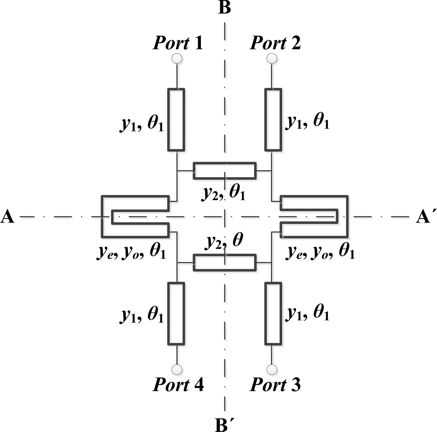
Fig. 1. The proposed dual-band quadrature hybrid with arbitrary power division ratios.
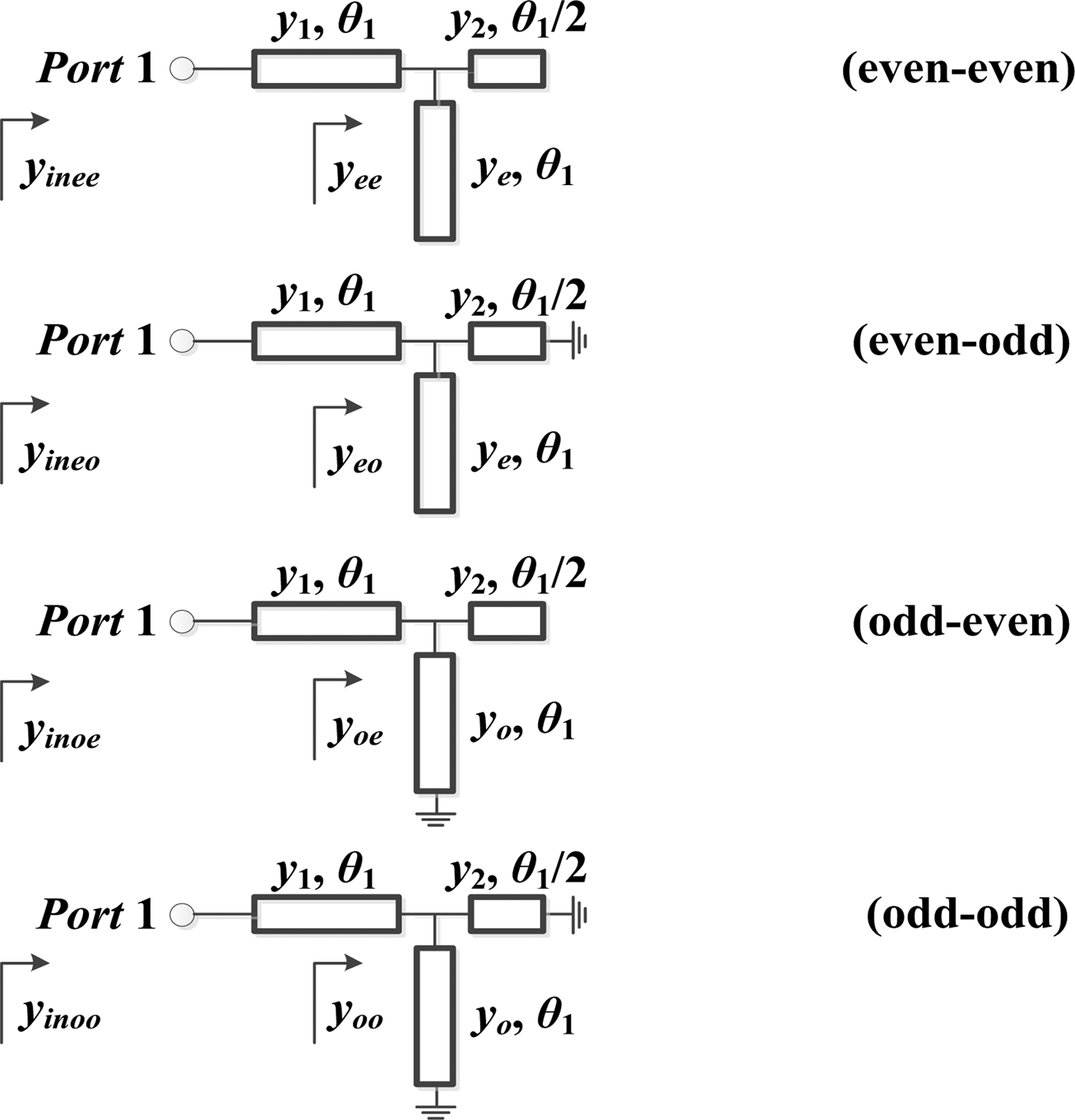
The bisymmetrical structure along the AA′ and BB′ axes facilitates the use of even–odd decomposition analysis method, delineated in [Reference Collin17]. These two lines divide the circuit into quarter circuit sections shown in Fig. 2.

Fig. 2. Four equivalent quarter circuits for the proposed quadrature hybrid.
The derivation of scattering parameters method from four quarter circuits, as presented in [Reference Collin17], is used to obtain the unknown parameters as follows.
 $${S_{11}} = {S_{22}} = {S_{33}} = {S_{44}} = \displaystyle{{{\Gamma _{ee}} + {\Gamma _{eo}} + {\Gamma _{oe}} + {\Gamma _{oo}}} \over 4}, $$
 $${S_{21}} = {S_{12}} = {S_{43}} = {S_{34}} = \displaystyle{{{\Gamma _{ee}} - {\Gamma _{eo}} + {\Gamma _{oe}} - {\Gamma _{oo}}} \over 4}, $$
 $${S_{31}} = {S_{42}} = {S_{13}} = {S_{24}} = \displaystyle{{{\Gamma _{ee}} - {\Gamma _{eo}} - {\Gamma _{oe}} + {\Gamma _{oo}}} \over 4}, $$
 $${S_{41}} = {S_{32}} = {S_{23}} = {S_{14}} = \displaystyle{{{\Gamma _{ee}} + {\Gamma _{eo}} - {\Gamma _{oe}} - {\Gamma _{oo}}} \over 4}, $$
where Γ ee , Γ eo , Γ oe , and Γ oo are the input reflection coefficients for the even–even-, even–odd-, odd–even-, and odd–odd-mode equivalent circuits, respectively, as shown in Fig. 2 and they can be calculated as
 $${\Gamma _{ab}} = \displaystyle{{1 - {y_{inab}}} \over {1 + {y_{inab}}}},\; \quad {\rm for}\,a, b = e\,\,{\rm or}\,\,o,$$
where
 $${y_{inab}} = {y_1}\displaystyle{{{y_{ab}} + j{y_1}\tan ({\theta _1})} \over {{y_1} + j{y_{ab}}\tan ({\theta _1})}},\quad {\rm for}\,a,\,b = e\,\,{\rm or}\,\,o,$$
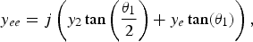 $${y_{ee}} = j\left( {{y_2}\tan \left( {\displaystyle{{{\theta _1}} \over 2}} \right) + {y_e}\tan ({\theta _1})} \right), $$
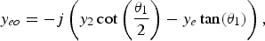 $${y_{eo}} = - j\left( {{y_2}\cot \left( {\displaystyle{{{\theta _1}} \over 2}} \right) - {y_e}\tan ({\theta _1})} \right), $$
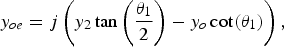 $${y_{oe}} = j\left( {{y_2}\tan \left( {\displaystyle{{{\theta _1}} \over 2}} \right) - {y_o}\cot ({\theta _1})} \right), $$
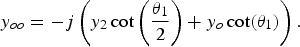 $${y_{oo}} = - j\left( {{y_2}\cot \left( {\displaystyle{{{\theta _1}} \over 2}} \right) + {y_o}\cot ({\theta _1})} \right).$$
A) Analysis of the circuit with vertical isolation
Looking at the 2D circuit structure in Fig. 1, for port isolation in vertical direction and perfect input–output matching, the required conditions are S 41 = S 32 = S 23 = S 14 = 0 and S 11 = S 22 = S 33 = S 44 = 0. Thus, from (1a) and (1d), the following equations are derived based on perfect port isolation and input–output matching.
 $${\Gamma _{ee}} + {\Gamma _{eo}} = 0,$$
 $${\Gamma _{oe}} + {\Gamma _{oo}} = 0.$$
For unequal output power division and 90° phase difference between output ports, one can obtain the following equation from (1b) and (1c).
 $${\Gamma _{ee}} - {\Gamma _{eo}} + {\Gamma _{oe}} - {\Gamma _{oo}} - jk({\Gamma _{ee}} - {\Gamma _{eo}} - {\Gamma _{oe}} + {\Gamma _{oo}}) = 0,$$
where k = |S 21/S 31| and k 2 is the power-dividing ratio between the output ports.
Substituting (2) into (5)–(7), these equations can be simplified as
 $${y_{inee}} \cdot {y_{ineo}} = 1,$$
 $${y_{inoe}} \cdot {y_{inoo}} = 1,$$
 $$k(1 - {y_{inee}}{y_{inoo}}) - j({y_{inee}} - {y_{inoo}}) = 0.$$
By solving (8)–(10), simultaneously, y 2, y e , and y o are obtained as
 $${y_2} = \displaystyle{{\sqrt {1 + {k^2}} y_1^2 \sin ({\theta _1})} \over {k\left( {{{\tan} ^2}({\theta _1}) + y_1^2} \right){{\cos} ^2}({\theta _1})}},$$
 $${y_e} = \displaystyle{{{y_1}\left( {2{y_1}\left( {\sqrt {1 + {k^2}} \cos \left( {{\theta _1}} \right) + 1} \right) - k\left( {y_1^2 - 1} \right)\sin \left( {2{\theta _1}} \right)} \right)} \over {k\left( {1 + y_1^2 + \left( {y_1^2 - 1} \right)\cos \left( {2{\theta _1}} \right)} \right)\tan \left( {{\theta _1}} \right)}},$$
 $${y_o} = \displaystyle{{{y_1}\left( {n{y_1}\sec \left( {{\theta _1}} \right) + 2k\sqrt {1 + {k^2}} \left( {y_1^2 - 1} \right)\tan \left( {\displaystyle{{{\theta _1}} \over 2}} \right)} \right)} \over {k\sqrt {1 + {k^2}} \left( {y_1^2 + {{\tan} ^2}\left( {{\theta _1}} \right)} \right)\left( {1 - {{\tan} ^2}\left( {\displaystyle{{{\theta _1}} \over 2}} \right)} \right)\cot \left( {{\theta _1}} \right)}},$$
where
 $$n = \sqrt {1 + {k^2}} {\sec ^2}\left( {\displaystyle{{{\theta _1}} \over 2}} \right) - \left( {1 + {k^2}} \right)\left( {1 - {{\tan} ^2}\left( {\displaystyle{{{\theta _1}} \over 2}} \right)} \right).$$
The θ 1 electrical length is chosen at the lower frequency as [Reference Park12]
 $${\theta _1} = \displaystyle{\pi \over {\left( {1 + {f_2}/{f_1}} \right)}},$$
where f 1 is the lower frequency band and f 2 is the upper frequency band.
B) Analysis of the circuit with horizontal isolation
Also, looking at the 2D circuit structure in Fig. 1, for isolation in horizontal direction and perfect input–output matching, the required conditions are S 21 = S 12 = S 43 = S 34 = 0 and S 11 = S 22 = S 33 = S 44 = 0. Thus, from (1a) and (1b), the following equations are derived based on the perfect port isolation and input–output matching.
 $${\Gamma _{ee}} + {\Gamma _{oe}} = 0,$$
 $${\Gamma _{eo}} + {\Gamma _{oo}} = 0.$$
For unequal output power division and 90° phase difference between output ports, one can obtain the following equation from (1c) and (1d).
 $${\Gamma _{ee}} + {\Gamma _{eo}} - {\Gamma _{oe}} - {\Gamma _{oo}} - jk\left( {{\Gamma _{ee}} - {\Gamma _{eo}} - {\Gamma _{oe}} + {\Gamma _{oo}}} \right) = 0,$$
where k = |S 41/S 31| and k 2 is the power-dividing ratio between the output ports.
Substituting (2) into (16)–(18), these equations can be simplified as
 $${y_{inee}} \cdot {y_{inoe}} = 1,$$
 $${y_{ineo}} \cdot {y_{inoo}} = 1,$$
 $$k(1 - {y_{inee}}{y_{inoo}}) - j({y_{inee}} - {y_{inoo}}) = 0.$$
By solving (19)–(21), simultaneously, y 2, y e , and y o are obtained as
 $${y_2} = \displaystyle{{y_1^2 \sin ({\theta _1})} \over {k\left( {{{\tan} ^2}({\theta _1}) + y_1^2} \right){{\cos} ^2}({\theta _1})}},$$
 $${y_e} = \displaystyle{{{y_1}\left( {2{y_1}\left( {\cos \left( {{\theta _1}} \right) + \sqrt {1 + {k^2}}} \right) - k\left( {y_1^2 - 1} \right)\sin \left( {2{\theta _1}} \right)} \right)} \over {k\left( {1 + y_1^2 + \left( {y_1^2 - 1} \right)\cos \left( {2{\theta _1}} \right)} \right)\tan \left( {{\theta _1}} \right)}},$$
 $${y_o} = - {y_e}\;{\tan ^{2}}\left( {{\theta _1}} \right) + 2\displaystyle{{y_{1}^{2} \sqrt {1 + {k^{2}}} \tan \left( {{\theta_{1}}} \right)} \over {k\left( {y_{1}^{2} + {{\tan}^{2}}\left( {{\theta_{1}}} \right)} \right){{\cos}^{2}}\left( {{\theta_{1}}} \right)}}.$$
The θ 1 electrical length is chosen at the lower frequency as [Reference Park12]
 $${\theta _1} = \displaystyle{\pi \over {\left( {1 + {f_2}/{f_1}} \right)}},$$
where f 1 is the lower frequency band and f 2 is the upper frequency band.
III. PRACTICAL LIMITATIONS
In order to implement the proposed coupler, the impedance values must be within the range of fabrication limitations for transmission line impedance (20–150 Ω) and this issue confines the operating frequency range and power division ratios of the proposed circuit. In the proposed circuit, four parameters (f 1, f 2, k, y 1) are chosen as free variables and by assigning proper values to them, we can implement a practical circuit. For convenience, let us define the equivalent admittance and coupling coefficient of the coupled lines as (26) and (27), respectively.
 $${y_{eq}} = \sqrt {{y_e} \cdot {y_o}}, $$
 $$C = 20\log \displaystyle{{{y_o} + {y_e}} \over {{y_o} - {y_e}}}.$$
Now, we examine the limitations for the two isolation conditions, separately.
A) Vertical isolation condition
Figure 3 shows the region plot of practical range of f 2/f 1 with different k and y 1 values, whereas the minimum coupling coefficient for coupled lines is 12 dB and y eq, y 1, and y 2 can vary from 0.34 to 2.5. Under these conditions, it is observed that the power dividing ratio up to 25 can be attained in a wide range of frequency ratios from 1.9 to 2.6. One other limitation that should be taken into account is the bandwidth of the proposed coupler. The bandwidth is mainly restricted by the amplitude balance and this problem becomes far more serious at the lower frequency band ratios and lower power dividing ratios. We can partially overcome this problem by using the lower value of coupling coefficient, such that the lower the value of coupling coefficient, the higher the bandwidth. Figure 4 shows the calculated value of |S 21| and |S 31| of the proposed coupler with different coupling coefficient of the coupled lines. In Fig. 4(a), it is observed that under the condition of |S 21|–|S 31| = 6 ± 1 dB, the bandwidth with C = 12 dB and uncoupled lines is 100 and 75 MHz, respectively. In Fig. 4(b), it is observed that under the condition of |S 21|–|S 31| = 12 ± 1 dB, the bandwidth with C = 12 dB and uncoupled lines is 120 and 95 MHz, respectively. In Fig. 4(c), it is observed that under the condition of |S 21|–|S 31| = 6 ± 0.3 dB, the bandwidth with C = 12 dB and uncoupled lines is 190 and 100 MHz, respectively. In Fig. 4(d), it is observed that under the condition of |S 21|–|S 31| = 12 ± 0.3 dB, the bandwidth with C = 12 dB and uncoupled lines is 260 and 180 MHz, respectively. Hence, if the minimum practical coupling coefficient is selected as C = 12 dB, the value of y 1 can be attained as
 $${y_1} = \displaystyle{{p + \sqrt {{p^2} + 4{k^2}{{\left( {4 + \cos (2{\theta _1})} \right)}^2}}} \over {2k\left( {4 + \cos (2{\theta _1})} \right)}},$$
where
 $$p = \sqrt {1 + {k^2}} \left( {4 + \cos (2{\theta _1})} \right)\csc ({\theta _1}) + 5\cot ({\theta _1}) - 3\tan ({\theta _1}).$$

Fig. 3. Region plot of practical range of f 2/f 1 with different k and y 1 for the proposed coupler with vertical isolation condition.

Fig. 4. Calculated |S 21| and |S 31| for different coupling coefficient of coupled lines. (a) f 1 = 1, f 2 = 1.8, and k = 2. (b) f 1 = 1, f 2 = 1.8, and k = 4. (c) f 1 = 1, f 2 = 3.4, and k = 2. (d) f 1 = 1, f 2 = 3.4, and k = 4.
Figure 5 plots the normalized admittances versus frequency band ratios with different power-dividing ratios, while the coupling coefficient for coupled lines is 12 dB.

Fig. 5. Normalized admittances versus frequency ratio with C = 12 dB and different power division ratios for the proposed coupler with vertical isolation condition.
B) Horizontal isolation condition
Figure 6 shows the region plot of practical range of f 2/f 1 with different k and y 1 values, whereas the minimum coupling coefficient for coupled lines is 12 dB and y eq , y 1, and y 2 can vary from 0.34 to 2.5. It is observed that the maximum achievable power dividing ratio for this circuit is 6.25, while the frequency band ratio is from 2.2 to 3.8. The bandwidth limitation factor for this circuit is exactly the same as the circuit with vertical isolation condition. Thus, if the lower value of coupling coefficient for coupled lines is selected, wider bandwidth can be achieved.

Fig. 6. Region plot of practical range of f 2/f 1 with different k and y 1 for the proposed coupler with horizontal isolation condition.
By setting C = 12 dB, the value of y 1 for horizontal isolation condition can be attained as
 $${y_1} = \displaystyle{{q + \sqrt {{q^2} + {k^2}{{\left( {8\sin (2{\theta _1}) + \sin (4{\theta _1})} \right)}^2}}} \over {k\left( {8\sin (2{\theta _1}) + \sin (4{\theta _1})} \right)}},$$
where
 $$q = \sqrt {1 + {k^2}} \left( {2 + 8\cos (2{\theta _1})} \right) + 9\cos ({\theta _1}) + \cos (3{\theta _1}).$$
Figure 7 plots the normalized admittances versus frequency band ratios with various power division ratios and C = 12 dB.

Fig. 7. Normalized admittances versus frequency ratio with C = 12 dB and different power division ratios for the proposed coupler with horizontal isolation condition.
IV. SPECIAL CASES
In this section, some interesting special cases of this circuit are discussed and their equations can be derived from the equations in this paper.
For special cases, assume that y 1 = k = 1. Hence, for the circuit with port isolation in vertical direction, (11)–(14) can be simplified as
 $${y_2} = \sqrt 2 \sin \left( {{\theta _1}} \right),$$
 $${y_e} = \left( {1 + \sqrt 2 \cos ({\theta _1})} \right)\cot ({\theta _1}),$$
 $${y_o} = - \sqrt 2 \sin ({\theta _1}) + \tan ({\theta _1}).$$
Also, for the circuit with port isolation in horizontal direction, (22)–(24) can be simplified as
 $${y_2} = \sin ({\theta _1}),$$
 $${y_e} = \left( {\sqrt 2 + \cos ({\theta _1})} \right)\cot ({\theta _1}),$$
 $${y_o} = \left( {\sqrt 2 - \cos ({\theta _1})} \right)\tan ({\theta _1}).$$
Based on these simplified equations, the especial cases are summarized as follows.
-
Case (1): In the case of vertical isolation, if we choose y e = y o , we can find from (33) and (34) that θ 1 = π/2.81. This case was presented as a dual-band circuit without any stubs in [Reference Park12]. Also, this case was presented as a branch-line coupler with unequal line lengths in [Reference Toker, Saglam and Ozme18].
-
Case (2): In the case of horizontal isolation, if we choose y e = y o, from (36) and (37), θ 1 = π/3.19 can be derived. This case was presented as a dual-band circuit without any stubs in [Reference Park12]. Also, this case was presented as a branch-line coupler with unequal line lengths in [Reference Toker, Saglam and Ozme18].
-
Case (3): The circuit with horizontal isolation was presented in [Reference Yu, Cheng and Pang9] as a 3-dB dual-band branch-line coupler and its equations are simplified as (32)–(34).
V. SIMULATION AND MEASUREMENT RESULTS
In order to verify the proposed method and its equations, two dual-band circuits have been simulated based on the ideal components. One of them features port isolation in the vertical direction and the other one in the horizontal direction. Ideal frequency responses for these circuits have been illustrated in Figs 8 and 9. The initial values for the circuit with vertical isolation are f 1 = 1, f 2 = 2.7, k = 3, and C = 12 dB to have the maximum achievable bandwidth. Based on these initial values, the other parameters are obtained from (11)–(15), (28), and (29) as y 1 = 1.99, y 2 = 1.368, y e = 0.443, y o = 0.738, and θ 1 = 48.65° at the lower frequency. Also, for the circuit with horizontal isolation, we have f 1 = 1, f 2 = 3.5, k = 1.5, and C = 12 dB to have the maximum achievable bandwidth. Based on these initial values, the other parameters are obtained from (22)–(25), (30), and (31) as y 1 = 2.44, y 2 = 0.653, y e = 1.296, y o = 2.16, and θ 1 = 40° at the lower frequency.

Fig. 8. Ideal responses for the dual-band circuit with isolation in vertical direction. (a) Scattering parameters. (b) Phase difference between ports 2 and 3.

Fig. 9. Ideal responses for the dual-band circuit with isolation in horizontal direction. (a) Scattering parameters. (b) Phase difference between ports 4 and 3.
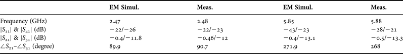
A dual-band coupler operating at f 1 = 2.45 and f 2 = 5.8 (wireless local area network (WLAN) frequencies) and k = 4 is designed, fabricated, and measured. The normalized admittances of each line sections are calculated as y 1 = 1.812, y 2 = 1.5, y e = 0.351, y o = 0.585, and θ 1 = 53.45° at the lower frequency. The coupling coefficient of coupled lines is set to 12 dB to have the maximum achievable bandwidth. Dielectric substrate (Rogers RO4003C) with thickness of 0.508 mm, dielectric constant of 3.38, and loss tangent of 0.0021 has been used for fabrication. Figure 10 shows the layout of the fabricated coupler with all the physical dimensions. The measured and simulated scattering parameters and output phase difference are shown in Fig. 11 with good consistency. Measurement of scattering parameters over the frequency range of 1–7.5 GHz was performed using Agilent E8361C vector network analyzer and the electromagnetic (EM) simulation was conducted using Agilent's ADS Electromagnetic simulator (EM Simulator) software. The summaries of simulation and experimental results are listed in Tables 1 and 2. Table 3 lists a comprehensive performance comparison of some recently published designs.

Fig. 10. Layout of the fabricated coupler W 1 = 2.7, W 2 = 0.19, W 3 = 2.1, S = 0.4, r = 3.3, L 1 = 12.06, and L 2 = 10.4 (all in millimeters).

Fig. 11. Simulated versus measured scattering parameters of the fabricated coupler. (a) Return loss and port isolation. (b) Insertion loss. (c) Output phase difference.
Table 1. Comparison between simulation and measurement results.

Table 2. Bandwidth (%) of the fabricated dual-band coupler.

Table 3. Performance comparison of some dual-band branch-line couplers with arbitrary power division ratios.

VI. CONCLUSION
In this paper, a novel design of generalized dual-band quadrature hybrid was proposed. The closed-form equations and circuit topology indicated that under certain circumstances, some of the recently published papers can be considered as special cases of the proposed structure. Moreover, the proposed structure provided very large power dividing ratios at dual frequency bands while retaining large frequency band ratios. Coupled lines with small coupling coefficient were utilized to obtain higher operating bandwidth at the two designated frequencies. The microstrip implementation of 16:1, 2.45/5.8 GHz dual-band coupler and good correlation between simulated and measured results substantiate the proposed method and the equations.
 Seyed-Ali Malakooti was born in Tehran Province, Tehran, Iran, in 1987. He received his B.S. and M.S. degrees in Electrical Engineering from Razi University, Kermanshah, Iran, in 2010 and 2013, respectively. His current research interests include design of microstrip antennas, multi-band passive microwave components, and digital integrated circuits.
 Mohsen Hayati received his B.E. degree in Electronics and Communication Engineering from Nagarjuna University, Nagarjuna Nagar, India, in 1985, and the M.E. and Ph.D. degrees in Electronics Engineering from Delhi University, Delhi, India, in 1987 and 1992, respectively. In 1993, he joined the Electrical Engineering Department, Razi University, Kermanshah, Iran, as an Assistant Professor. He is currently a Full Professor with the Electrical Engineering Department, Kermanshah Branch, Islamic Azad University as well as Razi University. He has authored over 155 papers in international and domestic journals and conferences. His current research interests include microwave and millimeter-wave devices and circuits, application of computational intelligence, artificial neural networks, fuzzy systems, neuro-fuzzy systems, electronic circuit synthesis, modeling, and simulations.
 Veria Fahimi received his B.S. and M.S. degrees in Electrical Engineering from Razi University, Kermanshah, Iran in 2010 and 2012, respectively. In 2014, he joined Electric Power Distribution Co., Kermanshah, Iran. His current research interests are Image processing and RF/Microwave circuit design.
 Behnam Afzali was born in Kermanshah, Iran in 1988. He received his B.S. degree in Electronics Engineering in 2010 from Islamic Azad University, Kermanshah Branch, Kermanshah, Iran. Also he received his M.S. degree in Electronics Engineering in 2014 from Islamic Azad University, Science and Research Branch, Kermanshah, Iran. His current research interest is RF/Microwave circuit design.