


Introduction
Diplexers/multiplexers are important components in wireless communication systems that can separate the signals from the same input port to two or more different channels according to their own frequencies. With the stringent requirements in modern communication systems, it is demanded that they have small size, low loss, high isolation, flexible channel frequencies, and so on. Therefore, various kinds of diplexers/multiplexers have been developed for modern transceivers, such as substrate integrated waveguide (SIW) [Reference Zhou, Zhou and Wu1–Reference Song, Zhou, Chen, Iman, Patience and Fan3], cavity [Reference Nocella, Pelliccia, Farinelli, Sorrentino, Costa, Yufeng and Yanzhao4–Reference Qi, Li and Zeng7], slotline [Reference Liu, Xu, Zhang and Guan8, Reference Chen, Zhu, Bu and Cheng9], coplanar waveguide structure [Reference Zheng, Wei, Gao, Guo, Zhang, Jiang, Xu and Heng10], and microstrip [Reference Rezaei and Noori11–Reference Chen, Lin, Tseng and Chang24].
In order to avoid employing the combining network and reduce the size, the adoption of common resonator at the input is a good solution, and it acts as a T-junction and the first resonator for both channels. In [Reference Zhou, Zhou and Wu1], the common dual-mode (TE101 and TE201) cavity is applied for designing SIW diplexer, while the frequencies and channel responses are difficult to be separately designed. Moreover, the large size of SIW makes it unsuitable for miniaturized systems. To reduce the size, the common T-shaped resonator in [Reference Chuang and Wu15, Reference Guan, Yang, Liu and Zhu16] is used to design microstrip diplexers. But the channel frequencies and responses cannot be flexibly designed yet, which inevitably increases the design complexity. Recently, a centrally-loaded half wavelength (λ/2) uniform-impedance resonator (UIR) is developed for the input common resonator, and with the aid of loaded stub, the two channel filters can be separately designed. However, all employed resonators are λ/2 ones. They have to be folded in many times and distribute in many layers in the low-temperature co-fired ceramic, which reduces the unloaded quality factor (Qu) of the resonator and then increases the passband loss.
In this letter, a common stub-loaded stepped impedance resonator (SIR) is investigated and used as a common input resonator to design a diplexer with multiple transmission zeroes (TZs). The stub is loaded at the voltage-null point of third harmonic f 3 of the SIR. It can separately control fifth harmonic f 5 but has no effect on f 3 so that the two channels of the diplexer can be separately designed. The input feed position on the stub-loaded SIR can be properly designed to generate a common TZ between f 5 and f 3, which exists in both channel filtering responses. Meanwhile, the coupling schemes of two channels can generate a TZ at the passband frequency of the other channel filter. Due to the existing of multiple TZs, the selectivity and isolation of the proposed diplexer can be improved significantly.
Stub-loaded SIR
Figure 1(a) shows the configuration of the SIR, where Zi and li (i = 1 or 2) are the characteristic impedance and physical length of the transmission line, respectively. Figure 1(b) plots f 5/f 3 against u under different RZ, where RZ = Z 1/Z 2 and u = l 1/(l 1 + l 2). The zoomed illustration clearly shows the confluence of five curves. In this design, f 5 and f 3 are chosen for the two channels and they can be close to each other. Accordingly, RZ = 2.3 and u = 2/3 are selected. Once the total physical length is given, both f 5 and f 3 can be calculated. Meanwhile, the voltage-null point (red point in Fig. 1) of f 3 should be located on the section with Z 1 of the SIR and can be determined by (1) below [Reference Li, Chen, Qin, Lu and Bao25], where Im[Z in] = 0

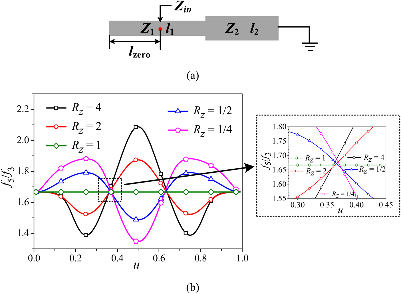
Fig. 1. (a) Traditional λ/4 SIR, (b) f 5/f 3 against u under different RZ and its zoomed illustration.
Substituting RZ = 2.3 and u = 2/3 into (1), uR = l 0/(l 1 + l 2) = 0.33 can be obtained.
To achieve the separate design of f 5 and f 3, a stub is attached to the voltage-null point of f 3 on the SIR, as shown in Fig. 2(a). It can be seen from Fig. 2(b) that as L stub or W 3 increases, f 5 shifts down and is gradually close to f 3 (fixed) so that the two close channels of the diplexer can be easily achieved. It can also be found that there is a TZ between f 3 and f 5, which depends on the location of feeding point (represented by L 2), as shown in Fig. 2(c). According to the transmission line theory, the input impedance Z int at the input port 1 can be expressed as

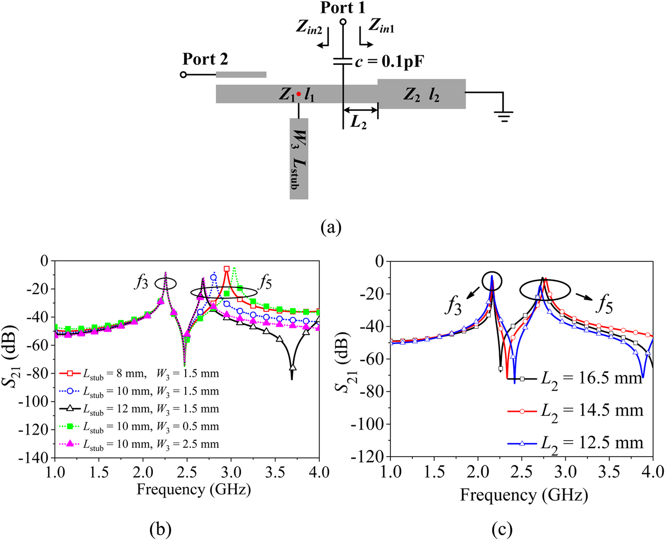
Fig. 2. (a) A weak coupling structure for analyzing the stub-loaded SIR, (b) frequency response against different stub length L stub and W 3 when L 2 = 14.5 mm and (c) different L 2 when L stub = 10 mm and W 3 = 1.5 mm.
Since the feeding point is at the right of the voltage-null point of f 3, the frequency f TZ of the TZ corresponding to Z int = 0 (due to Z in1 = 0) is larger than f 3. Similar to f 3, when the feeding point is located at the left of the voltage-null point of f 5, the f TZ can be smaller than f 5. As can be seen from Fig. 2(c), f TZ moves from f 3 to f 5 when L 2 increases. It is worthy to note that the TZ simultaneously exists in both channels so that the passband selectivity and isolation between the two channels can be enhanced greatly in the following design of diplexer.
Design of the proposed diplexer
Figure 3 shows the layout of the proposed diplexer. Port 1 is tap-connected to the common stub-loaded SIR operating at f 3 and f 5 for the lower and higher channels, respectively. The tapped position of Port 1 not only determines the location of the common TZ, but also affects the input external quality factor (Qe) of Port 1. A λ/4 UIR tapped by Port 2 (UIR1) couples with a part of common SIR to form the lower channel. The stub loaded at the voltage-null point of f 3 on the SIR is coupled with another λ/4 UIR tapped by Port 3 (UIR2) to construct the higher channel. In this design, the parameters of the UIRs can be optimized to achieve the desired Qes for both channels. Benefiting from the loading scheme of the common SIR, the stub can separately control f 5 but has no effect on f 3. As a result, the two channels of the proposed diplexer can be separately designed (as shown in Figs 5(a) and 7(a)) so that the respective specifications of the channels can be easily realized.

Fig. 3. Layout of the proposed diplexer.
Design of Qe at the common port (Port 1)
Due to the simultaneous impact of Qe and TZ by the tapped position of Port 1, the variation of input Qe (Qe 1) should be studied. When the Qe 1 is fixed, the Qes of the other two ports (Qe 2 for Port 2 and Qe 3 for Port 3) should meet the desired Qe, which is the value of Qe 1. Hence, the Qes of the three ports should be extracted.
The Qe can be extracted and attained by

where f 0 and f ±90° denote the central frequency and the ±90° bandwidth with respect to the absolute phase at f 0, respectively. The extracting procedures are as follow:
(1) Set the capacitor c = 0.1 pF to realize a weak coupling between feedline and resonator as shown in Fig. 2(a).
(2) Simulate the structure to obtain the phases in different f 0.
(3) Calculate the ±90° bandwidth of absolute phase at different f 0.
(4) Calculate Qes at different frequencies by using Eq. (3).
The Qe 1 under different L 2 is extracted and shown in Fig. 4. As can be seen, the variation trend of Qe 1 is different when the frequency changes. In this paper, the L 2 = 13.94 mm is chosen for the equivalent Qe 1 = 17 at f 3 and f 5. Hence, the equivalent fractional bandwidth (about 9%) of both channels can be achieved, which would be popular in practical applications.

Fig. 4. The Qe of Port 1 versus L 2 at the frequency of f 3 and f 5.
Design of the lower channel
For the lower channel filter operating in f 3 of the common SIR, the λ/4 UIR tapped by Port 3 coupled with the stub can be removed, as shown in Fig. 5(a). This is because the loaded stub has no effect on f 3 and can be ignored here. As expected, a TZ (TZ1 shown in Figs 5(b) and 5(c)) is obtained, resulting from the tapped feeding scheme of the common SIR. To achieve high isolation, another TZ (TZ2) is designed by using the parallel coupling structure with length L 5, which corresponds to the λ/4 at the frequency of TZ2. The TZ2 can be easily tuned by tuning L 5 and located in the upper channel, as shown in Fig. 5(c). Once L 5 is determined, the coupling coefficient between the SIR and UIR1 (K 12) can be controlled by the coupling gap g 2.

Fig. 5. (a) The structure of lower channel, (b) TZ1 changes with different length L 2 when L 5 = 13.7 mm, L 7 = 16.4 mm, W 2 = 0.5 mm, and g 2 = 0.1 mm, (c) TZ2 changes with different length L 5 when L 2 = 13.64 mm, L 7 = 16.4 mm, W 2 = 0.5 mm, and g 2 = 0.1 mm.
For constructing the lower channel, the Qe 2 should be equaled to the desired Qe 1 at the frequency of f 3. The Qe 2 are extracted and shown in Fig. 6. As can be seen, the tapped position of Port 2 (L 7) and the width of UIR1 (W 2) can be optimized to meet the desired Qe. As the desired Qe is obtained in Port 2, the desired K 12, which meets the requirement of 9% 3 dB fractional bandwidth, can be obtained by easily changing g 2. Until now, the lower channel has been constructed.

Fig. 6. The Qe of Port 2 versus different (a) L 7 when W 2 = 0.5 mm, (b) W 2 when L 7 = 1.64 mm.
Design of the higher channel
For the higher channel filter operating in f 5 of the common SIR, another λ/4 UIR tapped by Port 3 (UIR2) is used to couple with the stub. Since the loaded stub on the common SIR has no effect on f 3, it can be used to control the higher channel frequency alone. In this design, the UIR1 can also be removed, as shown in Fig. 7(a), because the coupling structure with length L 5 in the lower channel path can be regarded as an open circuit at f 5, indicated by TZ2 in Fig. 5. Similar to the lower channel filter, a TZ (TZ1 shown in Figs. 7(b) and 7(c)) is obtained, resulting from the tapped feeding scheme of the common SIR. To achieve high isolation, an extra TZ (TZ3) in the lower stopband can be generated, as shown in Fig. 7(c), and it can be optimized by tuning stub length L stub as well as the coupling length between the stub and UIR2 to be located in the lower channel.
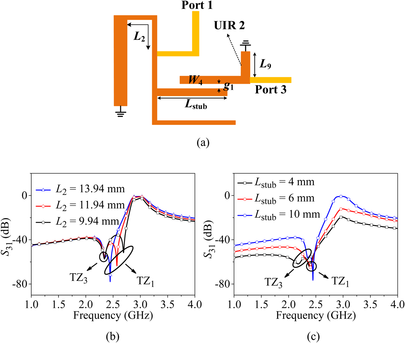
Fig. 7. (a) The structure of higher channel, (b) TZ1 changes with different length L 2 when L stub = 6 mm, W 4 = 1.5 mm, and g 1 = 0.4 mm, (c) TZ3 changes with different length L stub when L 2 = 11.94 mm, W 4 = 1.5 mm, and g 1 = 0.4 mm.
Similar to the design of Qe 2, the desired Qe can be also obtained by optimizing the tapped position of Port 3 (L 9) and the width of the UIR2 (W 4) for constructing the higher channel, as shown in Fig. 8. When the desired Qe is obtained in Port 3, the desired coupling coefficient between the SIR and UIR2 (K 13) can be obtained by easily changing g 1.

Fig. 8. The Qe of Port 3 versus different (a) L 9 when W 4 = 1.5 mm, (b) W 4 when L 9 = 1.75 mm.
The specific design procedures are as follows:
(1) According to the transmission line theory, the original frequency of f 3 and f 5 can be designed by choosing the appropriate length and Rz of the SIR. The f 5 can be altered to the desired frequency by changing the length and width of the loaded-stub (L stub and W 3);
(2) In order to produce a TZ between f 3 and f 5, the input line is tap-connected to the SIR as the feed point is loaded between the voltage-null point of f 3 and f 5. The TZ can be controlled by the location of the feed point;
(3) A λ/4 UIR is coupled to the open-end of the SIR to build the lower channel of the diplexer (at the frequency of f 3). An extra TZ (TZ2) can be generated and altered by the coupling length L 5. The desired Qe and K 12 can be obtained by the tapped-location of Port 2 (L 7), the width of the UIR1 (W 2), and the coupling gap (g 2).
(4) Similar to the design of the lower channel, another λ/4 UIR is coupled to the stub to build the higher channel of the diplexer (at the frequency of f 5). An extra TZ (TZ3) can be generated and altered by the L stub. The desired Q e and K 13 can be obtained by the tapped-location of Port 3 (L 9), the width of the UIR2 (W 4), and the coupling gap (g 1).
Based on the above analysis, the diplexer can be designed by combining the lower and higher channel filters, as shown in Fig. 3. By properly choosing the two coupled schemes and the feed position of the input port, each channel filter can generate two TZs in the vicinity of the other channel filter frequency, resulting in high selectivity and high isolation.
Simulated and measured results
The simulation and experiment of the proposed diplexer are conducted by using Ansoft HFSS and Agilent N5230A network analyzer, which can measure the mixed S parameters directly. Rogers RO4003c substrate with a dielectric constant of 3.38 and a thickness of 0.508 mm is used in this design. The structure parameters for the proposed diplexer are L 1 = 20 mm, L 2 = 13.94 mm, L 3 = 4.19 mm, L 4 = 5.55 mm, L 5 = 13.7 mm, L 6 = 17.24 mm, L 7 = 1.64 mm, L 8 = 11.84 mm, L 9 = 1.75 mm, L stub = 10 mm, W = 1.122 mm, W 1 = 2 mm, W 2 = 0.5 mm, W 3 = 1.5 mm, W 4 = 1.5 mm, d = 2.5 mm, g 1 = 0.4 mm, and g 2 = 0.1 mm. The photograph of the fabricated diplexer is shown in Fig. 9. Figure 10 shows the simulated and measured S parameter results of the proposed diplexer. The measured two passbands are centered at 2.28 and 2.95 GHz with the 3 dB fractional bandwidth of 8.9 and 9.3%. The insertion losses are 1.45 and 1.15 dB at the two center frequencies and the return losses in the two passbands are better than 12 dB. The common TZ1 between two channels is located at 2.46 GHz. The TZ2 and TZ3 in the lower and higher channel are located at 2.95 and 2.1 GHz, respectively, and then the isolations within the two passbands are better than 30 and 40 dB. The bandwidth of the lower channel in the measured result is smaller than that in the simulated result as shown in Fig. 10. That is because the coupling gap between the SIR and UIR1 (g 2 = 0.1 mm) is too small to guarantee the fabricated accuracy.

Fig. 9. The photograph of the fabricated diplexer.

Fig. 10. Simulated and measured results of the proposed diplexer.
Table 1 summarizes the performance comparison between the proposed design and the reported diplexer. It can be found that the proposed diplexer has low loss and simple design procedure due to the separate controlling of two bandpass response.
Table 1. Performance comparison with other previous diplexers

Conclusion
In this paper, a separately-designable diplexer with multiple TZs using a common stub-loaded SIR has been presented. Based on the stub-loaded stub and proper coupling scheme, the two channels can be separately designed, showing a simplified design method. Several TZs are generated to improve the selectivity and isolation. The proposed diplexer has been validated by the simulation and experiment. It owns several advantages such as low loss, good selectivity, and isolation, which would be a good candidate for many practical applications.
Acknowledgment
This work was supported by the Science-Technology Programs of Nantong, China (Grant No. MS12018004).
 Yu-Jing Zhang was born in Nantong, Jiangsu Province, China, in 1995. She received the B.Sc. Degree in electronic science and technology from Nantong University, Nantong, China, in 2017. She is currently pursuing the M.Sc. degree in electromagnetic field and microwave technology in Nantong University, Nantong, China. Her current research interests include microwave passive and reconfigurable filters.
 Jing Cai was born in Nantong, Jiangsu Province, China, in 1992. He received the B.Sc. degree in biomedical engineering from Nantong University, Nantong, China, in 2015, and the M.Sc. degree in information and communication engineering from Nantong University, Nantong, China, in 2018. His current research interests include microwave passive and reconfigurable filters.
 Jian-Xin Chen received the B.S. degree from Huai Yin Teachers College, Huai'an, China, in 2001, the M.S. degree from the University of Electronic Science and Technology of China (UESTC), Chengdu, China, in 2004, and the Ph.D. degree from the City University of Hong Kong, Hong Kong, in 2008. Since 2009, he has been with Nantong University, Nantong, China, where he is currently a Professor. He has authored or co-authored more than 100 academic papers. He holds 15 Chinese patents and three US patents. His research interests include RF/microwave differential circuits and antennas, dielectric resonator (DR) filters, and low-temperature co-fired ceramic circuits and antennas. Dr. Chen received the Best Paper Award presented at the Chinese National Microwave and Millimeter-Wave Symposium, Ningbo, China, in 2007. He was the Supervisor of 2014 iWEM student innovation competition winner in Sapporo, Japan.


