I. INTRODUCTION
The demand for using the unlicensed 60 GHz band for communication and radar applications is growing rapidly. The large available bandwidth in the 60 GHz band is appealing to high data rate multimedia communications. Furthermore, the 60 GHz band is very suitable for ultra-high-resolution imaging with short-range radar, thus it is attractive for such application as concealed weapon detection (CWD) [Reference Sheen, McMakin and Hall1]. These demands have motivated many developments in the 60 GHz systems, especially in the integrated 60 GHz front-end. The low-temperature co-fired ceramics (LTCC) technology provides an effective solution enabling integration of passive components including antennas and filters with MMICs in a single, cost-effective package. In addition, the multilayer nature of LTCC technology gives the possibility to realize three-dimensional structures such as cavities and vias. The passive components can then be placed at different layers, which enable miniaturization of modules. Therefore, the research of integrated LTCC antennas is very popular, such as in [Reference Vázquez, Holzwarth, Oikonomopoulos-Zachos and Rivera2–Reference Sun, Zhang, Chua, Wai, Liu and Gaucher4]. Challenges of realizing antennas with the LTCC material in the mm-wave region are related to fabrication accuracy and limitations on structures such as lines, metal plates, or vias. In addition, high relative permittivity of the LTCC material may limit the bandwidth of the antenna and supports excitation of the surface waves in the substrate. As a result, several attempts have been used to lower the effective dielectric constant such as using an air cavity [Reference Lamminen, Säily and Vimpari5, Reference Panther, Petosa, Stubbs and Kautio6] or punching holes [Reference Venot, Schuler and Wiesbeck7]. However, these approaches will complicate the manufacturing of the antenna, lower the yield rate, and increase cost. The operational bandwidth of LTCC antennas reported in literature is typically below 18% [Reference Panther, Petosa, Stubbs and Kautio6, Reference Methfessel8].
This paper presents a novel differentially fed UWB antenna for CWD imaging radar. The antenna should be manufactured using the LTCC technology to be ready for integration with 60 GHz MMICs for UWB front-end. To achieve sufficient down-range resolution and fully use capabilities of the front-end, the antenna operational bandwidth should be in excess of 15 GHz. Additionally, the antenna is required to have good radiation characteristics such as broadside uni-directional radiation patterns and the radiation patterns should be stable within the operational bandwidth. To allow direct integration with differential RF front-ends with 100 Ω output impedance, the antenna should be differentially fed. As no antenna has been found in literature to satisfy all these demands, a new antenna has been designed. The aperture stacked patch (ASP) antenna has been selected as the basic antenna type because it can provide reasonably large bandwidth (typically up to 18% in LTCC [Reference Panther, Petosa, Stubbs and Kautio6]), moderate gain, and low back radiation [Reference Targonski, Waterhouse and Pozar9]. In addition, the ASP antennas can be easily integrated with MMICs. However, conventional ASP antennas are single-end fed by using a microstrip line and do not posses a required relative bandwidth. Therefore, a novel differential feeding scheme that combines an H-shaped aperture with a parallel transmission line formed by pair of pins has been proposed to enable the antenna to be directly integrated with differential MMICs. A specific aperture shape (H-shape) has been selected to increase the antenna operational bandwidth. The dedicated shield following the ideas of [Reference Li, DeJean, Tentzeris, Papapolymerou and Laskar10] has been designed to suppress influence of the surface waves on the antenna radiation and to achieve the uni-directional radiations patterns. In order to measure the antenna radiation with traditional equipment with unbalanced feeding, a dedicated version of the antenna with a specially designed UWB balun has been developed.
II. ANTENNA DESIGN
A) Antenna geometry
It is challenging to realize UWB antennas using the LTCC materials, and one of the reasons is the high dielectric constant of LTCC materials. The antenna we propose avoids use of complex (and expensive for manufacturing) previously investigated techniques such as air-cavity or punching holes and demonstrates a larger than other LTCC antennas [Reference Lamminen, Säily and Vimpari5–Reference Venot, Schuler and Wiesbeck7] relative bandwidth. The antenna is based on an ASP antenna. Figures 1(a) and 1(b) show the layered view and side view of the proposed antenna. To feed antenna differentially, we have adopted the idea from [Reference Xue, Zhang and Chin11] where a parallel wire instead of a microstrip line is used to excite the aperture on the ground plane. In addition, the aperture is modified from conventional rectangular shape into an H-shape (Fig. 2) to give additional resonances, which increases the antenna impedance bandwidth [Reference Gao, Li, Leong and Yeo12].

Fig. 1. Antenna geometry: (a) layered view of the antenna and (b) side view of the antenna.

Fig. 2. Antenna feeding structure.
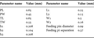
The antenna optimization is done numerically. A commercially available Electromagnetic (EM) solver Computer Simulation Technology (CST) MicroWave Studio (MWS) based on time domain finite integral technique has been used to develop the antenna numerical model and perform simulations. We performed a parametric study to investigate the influence of each antenna parameters (the antenna patch width, length, and aperture dimensions) on the impedance bandwidth. The detailed parametric study and final dimensions of the antenna can be found in [Reference Valavan, Yang, Yarovoy and Ligthart13]. The crucial antenna dimensions are shown in Table 1. Figure 3 shows the simulated optimized antenna reflection coefficient. The optimized antenna can achieve −10 dB impedance bandwidth from 50 to 78 GHz in simulations without any complicated structures such as air cavities or punching holes, which to the authors’ knowledge has never been reported in literature, especially for the differentially fed antennas.

Fig. 3. Simulated antenna reflection coefficient.
Table 1. Optimized parameters of the antenna.

B) Antenna radiation improvement
It is well known that for the patch-type antenna, the radiation characteristics can be significantly degraded by the diffraction of surface waves at the edge of the substrate, especially when the ε r of the substrate is high or the substrate size is large [Reference Li, DeJean, Tentzeris, Papapolymerou and Laskar10]. However, integrating the antenna with MMICs or adding structures such as balun for measurement purpose (Fig. 4(a)) will inevitably increase antenna size. This will cause the antenna radiation characteristics to degrade due to the strong surface wave. As a result, a semi-rectangular shield shown in Fig. 4(b) has been created to surround the antenna patches. This semi-rectangular wall consists of two via walls at the top and bottom of the antenna patches, two metal strips connecting the top and bottom walls, and the ground plane of the balun has been extended which acts as a back cap of the shield. Rectangular shield was selected due to its simplicity. The reason that two sides without via walls is to reduce the complexity and minimize the influence the cavity on antenna circuitry performance. To make the simulation comparable, both antenna models have same substrate size and same antenna structure, except the shielded antenna has slightly larger antenna ground plane (5.5 mm × 2.5 mm comparing to 3.5 mm × 2.5 mm). Simulation results (Figs 5(a) and 5(b)) showed that with this rectangular shield, the E-field is effectively confined within the shield. Thus, the edge diffraction effect of the surface wave on the gain and the radiation patterns can be alleviated. Figures 6(a) and 6(b) show the simulated radiation patterns of the unshielded and shielded antenna at 62 GHz. It can be seen that without the shield, the antenna radiation patterns have two strong side lobes. On the other hand, the radiation pattern of shielded antenna has one mainlobe with small sidelobes only. This demonstrates that with the shield, the antenna radiation patterns can be improved. Due to manufacturing limitations, the side wall of the shield is realized by interleaved connected vias. This technique has been proved to provide good emulation of solid vertical wall with vias of large pitch [Reference Yang, Vorobyov, Yarovoy, Ligthart, Rentsch and Muller14].

Fig. 4. Unshielded and shielded antenna: (a) antenna with balun but without shield and (b) antenna with balun and shield.

Fig. 5. Simulated E-field at the antenna surface at 60 GHz: (a) antenna without shield and (b) antenna with shield.

Fig. 6. Simulated radiation patterns of the unshielded antenna (a) and the shielded antenna (b) at 65 GHz.
C) Balun design
Since this antenna has differential feeding with input impedance of 100 Ω, it is not possible for us to measure it directly because differential measurement equipment that can work up to this frequency band is not available to us. Thus, a dedicated UWB balun shown in Fig. 7 was designed for the measurement purpose only (the balun is not included in the operational version of the antenna). This balun consists of a 50 Ω microstrip line input, and then the 50 Ω MS line connects to a two section Chebyshev impedance transformer to transform the impedance from 50 Ω MS line to a 25 Ω power combiner. The power combiner combines two 50 Ω MS lines with 180° phase difference. The two 180° phase difference lines are then connected to a coplanar strips with ground transmission line which connects to the antenna input. The simulation results showed that the balun provides less than −15 dB return loss and less than −1 dB insertion loss within the operational band, and the phase difference is 180 ± 30° between 55 and 65 GHz. The effect of this phase difference is that not only pure differential mode is excited, but also some common mode is excited. This result in the maximum radiation not radiated exactly at the z-direction but lean toward the x-direction. Figure 8 shows a comparison of simulated return loss of the antenna without balun, antenna with balun but without shield, and antenna with balun and shield. Several interesting features can be seen from this figure. Firstly, in the frequency range from 50 to 75 GHz, the reflection coefficient of the original antenna and the shielded antenna resembles each other, whereas the reflection coefficient of the unshielded antenna differs from the others. This demonstrates that the shield not only improves the radiation patterns, but also decreases the reflection coefficient. Secondly, there is an additional resonance at 81 GHz in the reflection coefficient of both the shielded and unshielded antenna with balun that enlarges the impedance bandwidth, but this resonance does not occur in the reflection coefficient of the original antenna. Therefore, we can conclude that this extra resonance is coming from the interaction between the balun and the antenna. However the antenna with balun is not intended to work up to 85 GHz as at such frequencies the balun no longer provides 180° phase shift, thus both common mode and differential mode will be excited, altering the antenna radiation characteristics.

Fig. 7. Layout of the balun.

Fig. 8. Comparison of simulated antenna reflection coefficient without balun, antenna with balun without shield, and antenna with balun and shield.
To realize the balun, a ground plane is necessary. The antenna itself has a ground plane at four layers (0.416 mm) below the feeding surface (h 3 in Fig. 1(b)), so ideally this ground plane should also be the ground plane of the balun. Unfortunately, 0.416 mm substrate thickness will lead to wide microstrip line width (about 0.683 mm for a 50 Ω MS line), and with this line width the 180° delay line will occupy a large area, which is a much undesired feature. As a result, we inserted an auxiliary ground plane at one layer (0.104 mm) below the feeding surface, thus the microstrip line width can be thinner (50 Ω MS line width reduces to 0.124 mm) and consequently the balun can occupy less space. By adding this auxiliary does not introduce any negative feature
III. EXPERIMENTAL VERIFICATION
The developed antennas have been manufactured to experimentally verify the simulated results. To keep the dielectric loss low, a material system optimized for high-frequency applications was employed, DuPont DP943® with tan δ = 0.002 specified for 40 GHz [15]. The measurement performed by manufacturer, Ilmenau University of Technology, revealed that the material has the real part of the dielectric permittivity of ε r = 7.54 and indicated an upper limit of tan δ = 0.01 at 60 GHz [Reference Alhouri, Rentsch, Stephan, Trabert, Müller and Hein16]. Figures 9(a) and 9(b) show the manufactured unshielded and shielded antenna. Due to manufacturing limitations, the ground plane of the balun has been realized using a 150 µm grid, but the ground plane of the antenna as well as the antenna patches are realized using solid metal to ensure proper operation of the antenna.

Fig. 9. Manufactured unshielded (a) and shielded antenna (b).
TRL calibration standards manufactured together with the antennas have been used to calibrate from the antenna connector to the microstrip line. Figure 10 shows the predicted and measured reflection coefficients of the unshielded and shielded antenna, respectively. Although in simulations it was predicted that the antennas have −10 dB reflection coefficient from 50 to 78 GHz, due to the measurement equipment limitations we can only measure up to 67 GHz. The measurement from the TRL standards showed that there is strong reflection from the connector, which is not able to be completely removed from the TRL calibration. Fortunately, large probing bandwidth enables us to separate the reflections from connectors in time domain. Thus the frequency domain measured data were transformed to time domain and use time gating technique to remove the unwanted connector reflections. This procedure, however, has decreased the upper frequency at which experimental results are reliable, to 65 GHz. The measured results showed that the shielded antenna has a −10 dB impedance bandwidth from about 51 GHz up to more than 65 GHz, and the −10 dB impedance bandwidth of the unshielded antenna is smaller, from 51.6 to 59.2 GHz. The predicted and measured reflection coefficients in general are in a good agreement with each other for both shielded and unshielded antenna. Some additional (with respect to simulations) resonances have been however observed. These resonances are mainly from the residue of the connector reflections. The better performance of the reflection coefficient of the shielded antenna demonstrates that the shield not only improves the radiation characteristics, but also provides better matching, which agrees with the results shown in Fig. 8. Although we were unable to measure the antenna up to 78 GHz (till the end of numerically predicted operational bandwidth), we trust the shielded antenna can behavior properly up to 78 GHz due to the good agreement between the predicted and measured results at the frequencies below 65 GHz.

Fig. 10. Simulated and measured reflection coefficient of the unshielded (a) and shielded antenna (b).
The antenna gain and radiation patterns were measured in mm-wave anechoic chamber with a standard gain horn. The gain and patterns are measured from 45 to 62 GHz. To measure the patterns, the antenna was mounted on a rotational cylinder. Due to the length limit of the cable, the patterns were only measured from −90 to 90°. Figure 11 shows the measured antenna broadside gain of the shielded and unshielded antenna. The gain was calculated by using three-antenna method. The gain of the shielded antenna is about 3.5–8 dBi in the band from 50 to 62 GHz. The gain of the unshielded antenna is considerably lower than that of the shielded antenna, from −5 to about 8 dBi. This demonstrates that with the shield, the antenna mainly radiates toward the broadside, while the maximum radiation direction of the unshielded antenna is unpredictable due to the influence of the surface wave. This statement is further justified by examining the antennas’ radiation patterns.

Fig. 11. Measured shielded and unshielded antenna gain at the broadside.
Figures 12 and 13 show the measured shielded and unshielded antenna radiation patterns at 50, 56, and 62 GHz, at their E-plane and H-plane, respectively. It can be clearly seen that for the shielded antenna, there is mainly one main lobe that radiates toward the broadside in both E-plane and H-plane, but for the unshielded antenna, the antenna radiates not toward the desired broadside direction but toward the side of the antenna. This is especially seen at the H-plane, because the antenna is greatly extended in the H-plane to accommodate the balun. The level of radiation patterns within ±30° (the area of interest with respect to the CWD imaging radar application) is within 5 dB, which is considered flat enough.

Fig. 12. Radiation patterns of the shielded antenna at the E-plane (a) and the H-plane (b).

Fig. 13. Radiation patterns of the unshielded antenna at the E-plane (a) and the H-plane (b).
IV. CONCLUSION
A novel LTCC differentially fed UWB ASP antenna operating in the 60 GHz range with more than 15 GHz impedance bandwidth and good radiation characteristics is presented. To achieve differential feeding with a large bandwidth, novel antenna feeding via an H-shaped aperture fed by a parallel transmission line has been developed. Special aperture shape also contributes to increase of the antenna operational bandwidth. To alleviate the influence of the surface wave (efficiently excited in LTCC due to the high value of the material dielectric constant) on the antenna radiation characteristics (such as altering the radiation patterns or raising sidelobes), a shield has been designed to surround the antenna patches. The antenna design is very simple; no complicated structures such as air cavities or punching holes have been used, which reduces the complexity and manufacturing costs. It has been demonstrated in simulations that with this feeding, the antenna can achieve a −10 dB impedance bandwidth from 50 to 78 GHz (the relative bandwidth of 44%). Thus the proposed antenna design is superior over known LTCC ASP antennas both in terms of performance and simplicity.
A dedicated version of the antenna (with integrated balun) has been developed and manufactured to verify the design experimentally. The measured results demonstrated that with the shield, the antenna outperforms the unshielded antenna in all aspects (impedance bandwidth, gain, and radiation patterns). The measured results showed that the −10 dB impedance of the shielded antenna starts from about 51 GHz and up to above 65 GHz (the highest frequency at which it was possible to measure). The good agreement between the predicted and measured results at the frequencies below 65 GHz makes us trust that the shielded antenna has impedance bandwidth up to 78 GHz (as in simulations). The antenna gain varies from 3.5 to 8 dBi within this frequency range, and the −5 dB beamwidth is about from −30 to 30° for both E- and H-planes. An integrated version of this antenna with MMIC has been designed but was not experimentally verified because the RF MMIC was unavailable at this moment.
ACKNOWLEDGEMENT
The authors would like to thank Alexander Schulz from Ilmenau University of Technology for manufacturing the antennas.
 Bill Yang received B.Sc. degree in communication engineering from Chiao Tung University, Hsin Chu, in 2002, and M.Sc. degree in Delft University of Technology, the Netherlands in 2006. Since 2006 he has been working on his Ph.D. degree in the International Research Center for Telecommunications and Radar (IRCTR) of Delft University of Technology, the Netherlands. His research interests include UWB antenna array design and signal processing for near-field imaging.
 Alexander G. Yarovoy graduated from the Kharkov State University, Ukraine, in 1984 with the diploma with honor in radiophysics and electronics. He received the Candidate Phys. & Math. Sci. and Doctor Phys. & Math. Sci. degrees in radiophysics in 1987 and 1994, respectively, at the Kharkov State University, and became a professor there in 1997. Since 1999 he is with the Delft University of Technology, the Netherlands where he leads since 2009 a chair of Microwave Technology and Systems for Radar. His main research interests are in ultra-wideband microwave technology and its applications (in particular, radars) and applied electromagnetics (in particular, UWB antennas). He has authored and co-authored some 250 scientific or technical papers, three patents and 14 book chapters. He is the recipient of a 1996 International Union of Radio Science “Young Scientists Award” and the European Microwave Week Radar Award in 2001 for the paper that best advances the state-of-the-art in radar technology (together with L.P. Ligthart and P. van Genderen). Prof. Yarovoy served as the Chair and TPC chair of the 5th European Radar Conference in 2008. He is a member of the Board of Directors of the European Microwave Association since 2008.
 Shenario Ezhil Valavan is from Madras, India. He completed his B.E. from Anna University in June 2006 and his M.S. (EE) from Delft University of Technology in April 2008. Currently, he is a Ph.D. student at IRCTR of Delft University of Technology. His research interests include phased array antennas, UWB, and antennas for radio astronomy.
 Koen Buisman received the M.Sc. degree in microelectronics from Delft University of Technology, Delft, The Netherlands, in 2004, and is currently working toward the Ph.D. degree at Delft University of Technology. Since 2004, he has been with the Delft Institute of Microsystems and Nanoelectronics (DIMES), Delft University of Technology. He was involved in the development of a pulsed DC and RF measurement system, an active harmonic load-pull system and the development of a custom in-house DIMES technology for high performance “distortion-free” varactors. His research interests are varactors for RF adaptivity, nonlinear device characterization, and compact modeling of heterojunction bipolar transistors. He has authored or coauthored over 25 papers.
 Oleksiy Shoykhetbrod was born in Odessa/Ukraine, in 1983. He received his diploma degree at University of Applied Sciences in Koblenz/Germany, in 2009, where he is currently working toward the master of system engineering degree. Since November 2009 he is also working at Fraunhofer Institute for High Frequency Physics and Radar Techniques FHR in Wachtberg. His current tasks involve simulation and measurement of the microwave and millimeter wave devices.