


I. INTRODUCTION
Slots in planar transmission lines, according to their radiation characteristics, may act as antennas [Reference Guha, Biswas, Biswas, Siddiqui and Antar1] or filters [Reference Ahn, Park, Kim, Qian and Itoh2]. In addition, they can provide high permeability as in slow wave transmission lines [Reference Safwat, Tretyakov and Raisanen3], and negative permeability as in electromagnetic (EM) band gap [Reference Hamad, Safwat and Omar4] and composite right-/left-handed structures [Reference Safwat5].
In the quest for compact size and low resonant slots, several shapes were proposed: rectangular dumbbell-shaped slot also known as “defected” ground structure (DGS) [Reference Guha, Biswas, Biswas, Siddiqui and Antar1], circular and arrow dumbbell [Reference Rahman, Verma, Boutejdar and Omar6], E, H, L, and U shapes [Reference Huang and Lee7–Reference Boutejdar, Batmanov, Awida, Burte and Omar10], and reconfigurable and tunable DGS [Reference Safwat, Podevin, Ferrari and Vilcot11–Reference El-Shaarawy, Coccetti, Plana, El-Said and Hashish13]. Although these structures shared common features, however, each one had a unique resonant behavior. Interestingly, correlation between these structures has not yet been investigated.
In terms of modeling, a simple RLC parallel resonant circuit was sufficient to capture the resonance behavior of the slot [Reference Guha, Biswas, Biswas, Siddiqui and Antar1]. However, this model could not describe the spurious frequencies that were attributed to the distributed nature of the slots [Reference Hong and Karyamapudi14]. Therefore, geometrical models based on transmission lines were proposed in [Reference Caloz, Okabe, Iwai and Itoh15–Reference Safwat, Tretyakov and Raisanen18] to explain the slot behavior over wide bandwidth. Yet and due to their complex configurations, several proposed slot shapes still lack simple geometrical circuit models.
In this paper, a systematic approach for designing and modeling letter-shaped microstrip ground slots is proposed. Twenty-three letters are patterned using 16 microstrip ground slots. For each letter, a geometrical circuit model is proposed. The structures are EM simulated and, in some cases, they are measured. Good agreement is achieved between EM and circuit simulations, and measurements. Interestingly, several characters have their own EM print.
II. THEORY
The proposed procedure of patterning a letter on the ground of a microstrip line, shown in Fig. 1(a), is very similar to the traditional seven-segment display, however, the seven segments are replaced by 16 segments as shown in Fig. 1(b). Each has 0.5 mm width. The length of the slot depends on its location. Slots in the transverse direction have 10 mm length, those in the longitudinal direction have 5 mm length, and those in the diagonal direction have 11.2 mm length. Letters are constructed using the appropriate combination of these slots, e.g. Fig. 1(c) shows letters A (eight slots) and K (four slots). In this paper, 23 letters are investigated. They are A, B, C, D, E, F, G, H, I, J, K, L, M, N, P, R, S, T, U, W, X, Y, and Z. Letters O, Q, and V are not studied since they look similar to letters D and U, respectively.

Fig. 1. (a) Conventional microstrip line, (b) locations of the slots to generate the letter-shaped structures, (c) letters A and K as drawn in HFSS.
The geometrical circuit models of these structures are divided, according to the type of the transition, into two categories. (1) Transitions with single mode where the slot is in the transverse direction, as shown in Fig. 2(a). This is a microstrip-to-slot line transition [Reference Safwat, Tretyakov and Raisanen18] as the current distribution on the ground indicates. (2) Transitions with two modes where the slot is in the longitudinal direction and it is etched beneath the strip symmetrically. Along the slot, the structure has three conductors, one on the top layer and two on the bottom layer, hence two modes that have even and odd symmetry, as shown in Fig. 3, can co-exist.

Fig. 2. (a) L-shaped slot, L 1 and L 2 (dotted lines) are the lengths of the two stubs, dark solid line shows the direction of the current, (b) equivalent circuit model, Z c, Z c,s are the characteristic impedances of the host line and slot line stub, respectively, and ɛ eff, ɛ eff,s are the effective dielectric constants of the host line and slot line stub, respectively.

Fig. 3. (a) Microstrip line with a slot in the longitudinal direction, (b) even and odd modes at the cross section AA′.
Simulations of the geometrical circuit models are shown in Figs 4 and 5, which also show the schematic of the letter in the inset. The height of the substrate is 1.6 mm and the relative dielectric constant is 4.4. The host microstrip line has 2.8 mm width and 40 mm length. For simplicity, both dielectric and conductor losses were neglected. To confirm the theory, the structures were simulated on the commercial EM software HFSS version13. The EM simulated s-parameters are also shown in Figs 4 and 5. The good agreement between the EM and circuit simulations indicates that the models are capable of capturing the main features of the structures. In the next sections, a quantitative description of the geometrical models is presented.

Fig. 4. Circuit versus EM simulations for different letter-shaped microstrip ground slots, the inset shows the structure schematic.
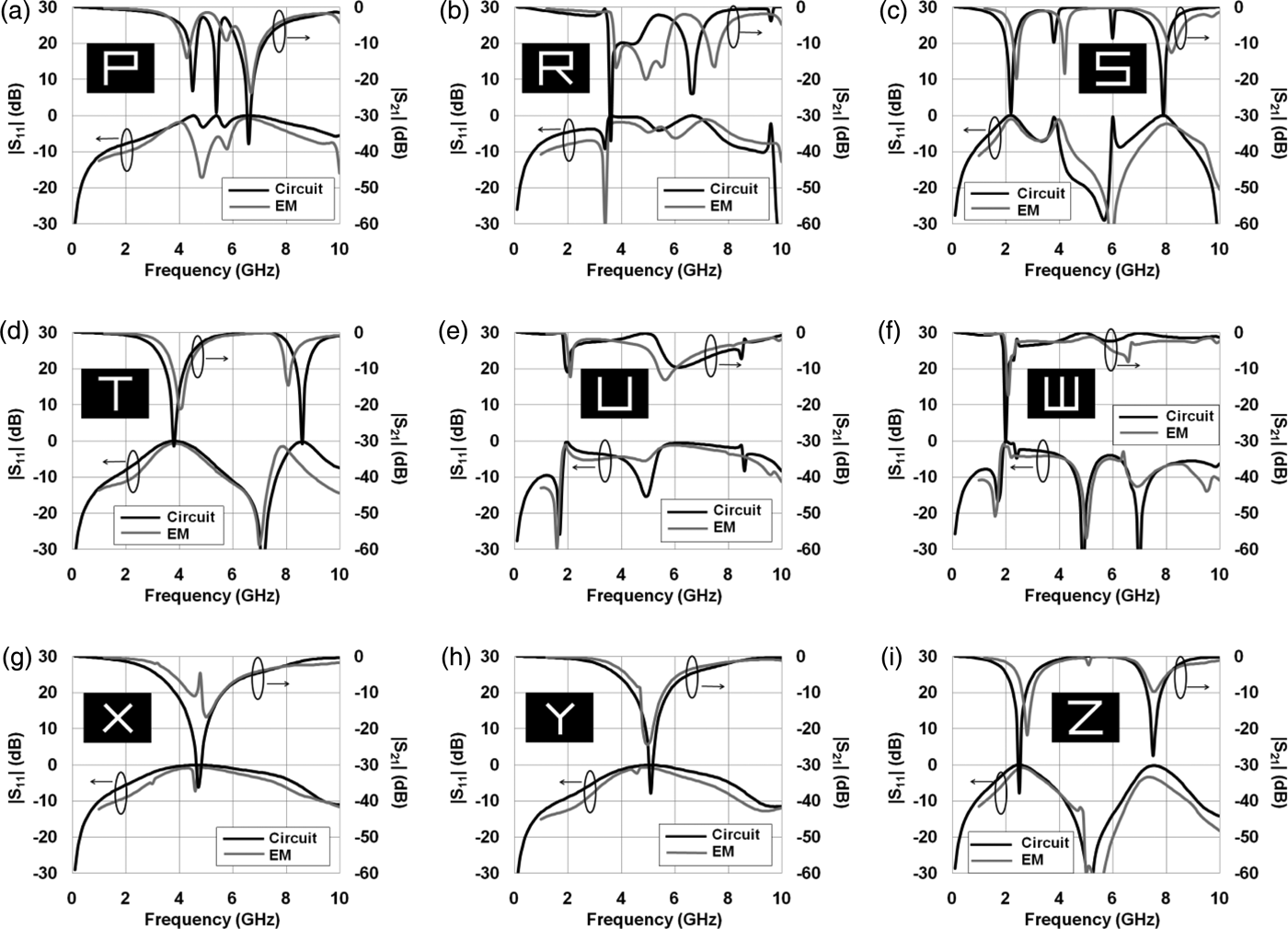
Fig. 5. Circuit versus EM simulations for the rest of the letter-shaped microstrip ground slots, the inset shows the schematic structure.
A) Category I: transitions with single mode
This category has the following letters: C, D, I, J, K, L, M, N, T, U, W, X, Y, and Z. Figure 2 shows the letter “L” when patterned on the ground. The current, shown in solid line, indicates two series stubs connected in parallel. In this case, the lengths of the stubs, L 1 and L 2, are 10 and 20 mm, respectively, and the characteristic impedance, Z c,s, is 100 Ω, and the effective dielectric constant, ɛ eff,s, is 2.3 corresponding to 0.5 mm slot width.
While the widths of the stubs are constant, their lengths and number depend on the letter. For example, letter C, shown in Fig. 4(c), has two identical stubs, similarly, are the letters I and Z, shown in Figs 4(g) and 5(i), respectively. Some letters have more than two stubs at the transition. Letter K has four stubs, two have 10 mm length and two have 11.2 mm length. They are parallel to each other and are connected in series to the host line. Letter X has four identical stubs each has 11.2 mm length, and letter Y has three stubs, two have 11.2 mm length and the third one has 10 mm length.
Some letters in this category have more than one transition. Letters M and U have two transitions and letters N and W have three transitions. Since there is a single mode at these transitions, the model still holds. For example, letter N has three transitions, separated by 5 mm. Each transition consists of two stubs connected in series to the transmission line and parallel to each other, i.e. there are six stubs connected together to form the letter N. Letter M has the same number of stubs, however, the connection is different. Similarly, is the case of letter W.
B) Category II: transitions with two modes
This category has the following letters: A, B, E, F, G, H, P, R, and S. They are all characterized by the presence of a slot beneath the strip symmetrically and in the longitudinal direction. Other slots are in the transverse direction and they form with the former slot a cross transition as shown in Fig. 6(a). The equivalent circuit of this transition relies on the present modes. As explained earlier, a slot in the longitudinal direction allows the generation of two modes that posses even and odd symmetry. At the cross transition, these two modes transform to the slot line mode and vice versa. By applying Kirchoff's current law and Kirchoff's voltage law as shown in Fig. 6(b) the following voltage and current equations are obtained:
 $$V_{sa} = \lpar V_{e\comma 2} - V_{e\comma 1} \rpar - {V_{o\comma 2} - V_{o\comma 1} \over 2}\comma \; \eqno\lpar 1\rpar$$
 $$V_{sb} = \lpar V_{e\comma 2} - V_{e\comma 1}\rpar + {V_{o\comma 2} - V_{o\comma 1} \over 2}\comma \; \eqno\lpar 2\rpar$$
 $$I_{sa}=I_{o\comma 2} - {I_{e\comma 2} \over 2} = - I_{o\comma 1} - {I_{e\comma 1} \over 2}\comma \; \eqno\lpar 3\rpar$$
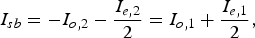 $$I_{sb} = - I_{o\comma 2} - {I_{e\comma 2} \over 2} = I_{o\comma 1} + {I_{e\comma 1} \over 2}\comma \; \eqno\lpar 4\rpar$$
where V e,1, V o,1, V e,2, and V o,2 are the even and odd voltages at ports 1 and 2, respectively, I e,1, I o,1, I e,2, and I o,2 are the even and odd currents at ports 1 and 2, respectively, V sa, V sb, I sa, and I sb are the voltages and currents at the two slot lines.
Fig. 6. (a) Microstrip line with cross slot, (b) voltages and currents distribution on the top and bottom conductors, for the sake of clarity the width of the slot is exaggerated to look wider than the strip, (c) equivalent circuit model of the transition.
These equations are identical to those presented in [Reference Ribo and Pradell19], where a coplanar waveguide (CPW) to slot line cross transition was proposed. This is expected since a microstrip on a slot can be seen as a CPW that has the center conductor located on the top layer of the substrate while the ground is located on the bottom layer. Accordingly, the equivalent circuit model proposed in [Reference Ribo and Pradell19] and shown in Fig. 6(c) corresponds to a microstrip-to-slot line cross transition as well.
This transition reduces to a simple microstrip-to-slot line one, category I, when the letters are symmetric with respect to the strip, e.g. letters B, E, and H. In these structures, the odd mode does not exist, and the slot, which lies beneath the strip, changes slightly the characteristic impedance of the transmission line that connects the two transitions. Nevertheless, this effect is negligible since the slot width is small. For 0.5 mm slot width the characteristic impedance of the host line, Z c, is 54 Ω, which is very close to a microstrip without slot, Z c is 52 Ω, and the effective dielectric constant, ɛ eff, which is equal to 3.4, does not change. This explains why letters B and E behave identical to letters D and C, respectively.
Letter F, shown in Fig. 4(d), is not symmetric with respect to the strip and, hence, the odd mode is generated. At the left transition, one port has a microstrip mode that has even symmetry, i.e. the odd mode is short circuited in the circuit model. The two slot lines in the transverse direction form two stubs of different lengths (20 and 10 mm, respectively). The other port, which has the slot in the longitudinal direction, has the even and odd modes. Their characteristic impedances, Z c,e and Z c,o, are 54 and 100 Ω, respectively, and their dielectric constants, ɛ eff,e and ɛ eff,o, are 3.4 and 2.3, respectively. The two modes propagate a distance that is equal to the length of the slot (10 mm = 2 × 5 mm). At its end, there is a second transition. The two slot lines have zero length and are short circuited, similarly is the odd mode, and the even mode transforms back to the microstrip mode.
Letter S, shown in Fig. 5(c), is similar to letter F. However at the left transition, there is one slot line, the other one is short circuited. The even and odd modes in the longitudinal slot propagate 10 mm (2 × 5 mm). At the second transition, there is also one slot line, the odd mode is short circuited, and the even mode transforms back to the microstrip mode.
Letters A, P, and R, shown in Figs 4(a), 5(a), and 5(b) respectively, are asymmetric as well. Hence, the odd mode is present. Moreover, they share an extra common feature that is the presence of a rectangular slot line loop that connects the two transitions. Three arms of the loop are slot lines, each has 10 mm length, and the fourth arm is the slot beneath the strip. Letter P is the basic structure in this group. It consists of the loop and a 10 mm length short-circuited slot line connected to the first transition. Letter A is identical to letter P except that it has an extra 10 mm slot line at the second transition. Letter R is similar to letter P, in addition it has a third transition located at the middle of the slot beneath the strip. Connected to this transition is an extra slot line that has 11.2 mm length.
Letter G, shown in Fig. 4(e), belongs to categories I and II. The first transition, the one at the left, is a simple microstrip-to-slot line transition, category I. The two slot lines form two stubs, one is short circuited and has 20 mm length and the second is connected to the third transition. The second transition is after 5 mm, the microstrip mode transforms to the even and odd modes due to the presence of the slot. At this transition, the slot lines have zero length and they are short circuited. The third transition appears after another 5 mm. One slot line has zero length, the second slot line, which has 30 mm length, is connected to the first transition, and the odd mode is short circuited.
C) Discussion
In general, the equivalent circuit models agree well with the EM simulations. However, little discrepancies appear in some simulations. These may be due to the following reasons: the circuit models are implemented on microstrip, while the slot lines are modeled as four-terminal transmission lines that have constant characteristic impedance and effective dielectric constant. Consequently, dispersion effects in slot lines are not considered. Also, the circuit models, and for the sake of simplicity, do not take into account the effect of the discontinuities, e.g. slot line bend. These simplifications result in a frequency shift between circuit and EM simulations. Fortunately, this effect appears in most of the structures after 6 GHz.
Dielectric and conductor losses are neglected in both circuit and EM simulations. However, in the latter the structures are surrounded by a radiation box, hence, radiation losses are included. This affects the magnitude of the s-parameters for letters B, D, and P as the presence of a closed loop increases radiation.
In letters X and Y, the slots are very close at the transition and, hence, they couple. The coupling reduces in the transverse direction because the separation between the slot lines increases. This coupling manifests itself as a notch in the s-parameters. Fortunately, the coupling is not significant as the notch is very small.
D) Applications
Several structures behave as band stop filters, e.g. letters C, E, I, X, and Z are single band stop filters, letters J, K, L, T, and Y are dual band stop filters, letters F, G, and S are triple band stop filters, and letter H is a wide band stop filter. Other letters, e.g. B, D, and P have good radiation characteristics. Due to the circuit models, novel applications can also be foreseen, e.g. a word that has a specific frequency response or new radio frequency identification (RFID) structures.
III. EXPERIMENTAL VERIFICATION
Six structures are fabricated on FR4 (h = 1.6 mm, ɛ r = 4.4, and tan δ = 0.02). They are: A, F, N, R, U, and X, i.e. three structures from category I and three structures from category II. In the EM simulations, both dielectric and conductor losses are included. Figure 7 shows the EM simulations and measurements. Very good agreement is achieved. Results are consistent with circuit simulations, which confirm the developed theory.

Fig. 7. EM simulations versus measurements, inset shows the fabricated structure.
IV. CONCLUSION
Twenty-three letter-shaped structures were patterned on microstrip ground. For every structure, a geometrical circuit model based on novel microstrip-to-slot line transitions was developed. Results were compared with EM simulations. Good agreement was observed. Among these structures, 21 have unique EM behavior (EM print). Six structures were fabricated and measured. Measurements are in a very good agreement with theory. This new concept may pave the way to realize other structures and new applications, e.g. EM-based character recognition or new RFID structures.
 Amr M. E. Safwat received the B.Sc. and M.Sc. from Ain Shams University in 1993 and 1997, respectively, and the Ph.D. from University of Maryland at College Park, in 2001 in electrical engineering. From August 2001 to August 2002, he was with Cascade Microtech Inc. In August 2002, he joined the Electronics and Communication Engineering Department, Ain Shams University, where he is currently an associate professor. Dr. Safwat had held visiting professor positions at the Otto-Von-Guericke University, Magdeburg, Germany (September 4–November 4), the “Institut National Polytechnique de Grenoble”, Grenoble, France (September 5–November 5), and the Radio Laboratory and MilliLab, Helsinki University of Technology, Finland (July 6–June 7). In 2008, he was awarded the Egyptian encouragement state prize for engineering sciences. His research interests include metamaterial, microwave passive planar structures, and microwave photonics.


