I. INTRODUCTION
Modern millimeter-wave and submillimeter-wave semi-conductor technologies with cut-off frequencies of more than 500 GHz [Reference Lai1–Reference Leuther3] are opening up new types of high-resolution active and passive imaging systems, high data rate wireless communication links as well as ultra-wideband transmitter and receiver components, e.g. for use in spectroscopy or measurement instrumentation. In comparison to visible and infrared radiation, a particular benefit of millimeter- and submillimeter-waves is the penetration of dust, fog, rain, snow, and even clothes. The favorably usable frequencies are around 94, 140, 220, 340, 410, 480, 660, and 850 GHz, where the transmission of the atmosphere exhibits local maxima. The higher operating frequency allows for precise geometrical resolution due to high absolute bandwidth and small wavelength. Furthermore, it reduces the size and weight of components and antennas, making them especially suitable for space and airborne systems. All of these applications raise the demand for low-noise amplifier MMICs with high gain, large bandwidth, and low-power consumption [Reference Samoska4–Reference Tessmann9].
High electron mobility transistors (HEMTs) are currently the most advanced devices for the next generation of millimeter- and submillimeter-wave monolithic integrated circuits (MMIC, S-MMIC). HEMTs deliver high gain at very high frequencies and produce the lowest noise figure of any active device. Several HEMT-based MMICs and S-MMICs operating at frequencies up to 700 GHz were published up to now [Reference Deal, Mei, Leong, Radisic, Sarkozy and Lai10, Reference Tessmann, Leuther, Massler and Seelmann-Eggebert11].
InP, GaAs, or even Si can be used as substrates for the epitaxial growth of InGaAs/InAlAs heterostructures. In the case of different lattice parameters in the substrate and the active device layers, the devices are called metamorphic HEMTs. Major advantages of the metamorphic approach are cost and quality of GaAs wafers as well as ease of the wafer handling.
For fabrication of integrated circuits operating up to 600 GHz and above, InGaAs/InAlAs metamorphic HEMT technologies with gate lengths of 100, 50, 35, and 20 nm based on 100-mm semi-insulating GaAs wafers have been developed at Fraunhofer IAF.
In this paper, we report on the development of two coplanar H-band (220–325 GHz) low-noise amplifier circuits, using our advanced 50 and 35 nm gate length metamorphic HEMT technologies. The utilized grounded coplanar waveguide (GCPW) technology is very attractive at millimeter-wave and submillimeter-wave frequencies, due to the high isolation between adjacent lines, the low source inductance of the active devices, and the suppression of unwanted substrate modes. For low-loss packaging of the amplifier circuits, a set of waveguide-to-microstrip transitions has been realized on 50-µm-thick GaAs substrates, covering the entire H-band frequency range from 220 to 325 GHz.
II. TECHNOLOGY
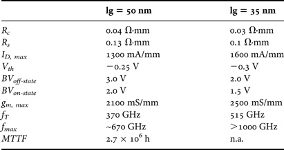
For fabrication of the amplifier MMICs, two metamorphic InAlAs/InGaAs based HEMT technologies have been employed [Reference Leuther3, Reference Leuther12]. The first technology features 50 nm gate-length in combination with an In0.52Al0.48As/In0.80Ga0.20As/In0.53Ga0.47As composite channel structure, resulting in an extrinsic transit frequency f T of 370 GHz and a maximum extrinsic transconductance g m, max of 2100 mS/mm. For the second metamorphic high electron mobility transistors (mHEMT) technology the gate length was reduced to 35 nm and a single InGaAs channel with an In content of 80% was used. These modifications result in an f T of more than 500 GHz and an extrinsic g m, max of 2500 mS/mm. The metamorphic HEMTs were grown on conventional 4″ semi-insulating GaAs wafers using molecular beam epitaxy (MBE). For the metamorphic buffer, a linear graded InxAl0.48Ga0.52-xAs (x = 0→ 0.52) transition was used. The gate definition of the 50 nm mHEMTs was performed using electron beam lithography in a four-layer resist (PMMA) process, whereas for the 35-nm devices the gate was defined in a two-step e-beam process. Additionally, the transistors are encapsulated in a low-k BCB layer to minimize the parasitic gate capacitance, and passivated with 250 nm chemical vapor deposited silicon nitride for good reliability and robustness. The electrical DC- and RF-parameters of the 50- and 35-nm mHEMT technology are summarized in Table 1.
Table 1. Electrical DC- and RF-parameters of the metamorphic HEMT technologies (w g = 2 × 10 µm).

Owing to the very compact design of the submillimeter-wave amplifier circuit, we had to adjust our grounded coplanar waveguide technology. Thus, the GCPW transmission lines were realized using the 300-nm-thick first metal only and the ground-to-ground spacing was reduced to 14 µm. To achieve a 50-Ω line impedance in this 14 µm environment a center conductor width of 7.4 µm was chosen. Furthermore, to suppress unwanted substrate modes, we developed a capacitor on via-hole process enabling the distribution of numerous through substrate vias over the entire chip area. Finally, the via-hole diameter was reduced from 35 to 20 µm.
III. H-BAND LOW-NOISE AMPLIFIER MMICS
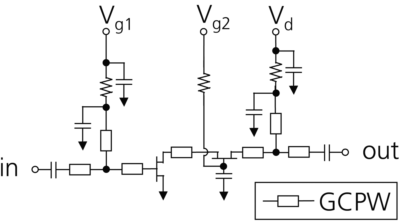
The four-stage H-band amplifier S-MMICs were designed to achieve high gain and large bandwidth in combination with very low-noise figure. Therefore, a cascode configuration, consisting of a series connection of one HEMT in common source and one in common gate configuration was utilized. The schematic diagram of a single cascode amplifier stage is shown in Fig. 1. The utilized transistors have a gate width of 2 × 10 µm.
Fig. 1. Schematic diagram of a single 243 GHz cascode amplifier stage (GCPW, grounded coplanar waveguide).
Figure 2 shows a chip photograph of the realized 50 nm H-band amplifier MMIC. The use of space saving grounded coplanar waveguide technology resulted in an over-all die size of only 0.5 × 1.5 mm2. On-wafer S-parameter measurements were performed using an Agilent PNA four-port network analyzer, two Oleson WR-3 T/R frequency extension modules and two Cascade i325 microwave probes. For an LRL-type calibration at the probe tip, a Cascade 138–356 calibration substrate was chosen.
Fig. 2. Chip photograph of the four-stage 50-nm H-band cascode amplifier MMIC. The chip size is 0.5 × 1.5 mm2.
A) Experimental results of 50-nm LNA MMIC
The simulated and on-wafer measured S-parameters of the four-stage 50 nm cascode amplifier circuit are depicted in Fig. 3, in the frequency range from 210 to 300 GHz. A linear gain of 31 dB was achieved at 243 GHz, by applying a drain voltage of V ds = 1.6 V, a second gate voltage of V g2 = 0.9 V, and a gate voltage of V g = 0.1 V. The total drain current at this bias point was I d = 35 mA. Between 218 and 280 GHz, we measured a small-signal gain of more than 28 dB. The input return loss S 11 and the output return loss S 22 were better than −10 dB at 243 GHz. The simulated noise figure at room-temperature (T = 293 K) was 5.1 dB at 243 GHz.
Fig. 3. Simulated and on-wafer measured S-parameters of the four-stage 50-nm H-band cascode MMIC amplifier (V ds = 1.6 V, V g2 = 0.9 V, V g = 0.1 V, I d = 35 mA).
B) Experimental results of 35 nm LNA MMIC
In addition to the 50 nm low-noise amplifier circuit, a 35-nm version was fabricated demonstrating increased gain performance, larger bandwidth and lower noise figure. As shown in Fig. 4, the 35-nm H-band amplifier MMIC achieved a small-signal gain of 35.7 dB at 243 GHz and more than 35 dB between 220 and 286 GHz, when applying a drain voltage of V d = 1.6 V, a second gate voltage of V g2 = 0.95 V, a gate voltage of V g = 0.15 V, and a drain current of I d = 31 mA (386 mA/mm). The strong ripple in the measured S-parameters is caused by unwanted crosstalk between the two RF-probes and disappears after packaging the millimeter-wave circuit into the waveguide module. The simulated room-temperature (T = 293 K) noise figure of the 35-nm LNA MMIC was 4.7 dB at 243 GHz.
Fig. 4. Simulated and on-wafer measured S-parameters of the four-stage 35-nm H-band cascode MMIC amplifier (V ds = 1.6 V, V g2 = 0.95 V, V g = 0.15 V, I d = 31 mA).
IV. WAVEGUIDE-TO-MICROSTRIP TRANSITIONS
In addition to the design of the H-band amplifier circuit, efforts were taken to develop a low-loss packaging solution for improved millimeter-wave performance. Thus, a set of H-band waveguide-to-microstrip transitions has been realized on 50-µm-thick GaAs substrates ensuring thickness compatibility with the LNA MMIC [Reference Hurm13]. Figure 5 shows a computer-aided design (CAD) drawing of the waveguide-to-microstrip transition in back-to-back configuration, which was optimized to cover the entire frequency range between 220 and 325 GHz. To couple the signal to and from the waveguide, a patch-antenna type probe was placed on the substrate, and aligned to the waveguide in longitudinal manner, i.e. along the direction of propagation. The backside metallization was removed on the part of the substrate, which protrudes into the waveguide.
Fig. 5. CAD drawing of a 50-µm-thick GaAs H-band waveguide-to-microstrip transition in back-to-back configuration.
To simulate the transitions, the high-frequency structure simulator HFSS of Ansys was used. The measured and simulated S-parameters of a GaAs transition in back-to-back configuration are shown in Fig. 6. We obtained an insertion loss S 21 of approximately 1 dB for two GaAs transitions in back-to-back configuration, leading to an insertion loss of approximately 0.5 dB for a single transition. The length of the microstrip line between the two GaAs transitions was 0.5 mm. The return loss S 11 and S 22 of the test structure stays well below 10 dB up to 325 GHz.
Fig. 6. Measured and simulated insertion loss (S 21) and return loss (S 11, S 22) of a 50-µm-thick GaAs (ε r = 12.9) H-band waveguide-to-microstrip transition in back-to-back configuration.
V. PACKAGING OF LOW-NOISE AMPLIFIER MODULES
A) Broadband 50 nm H-band low-noise amplifier module
For future use in a 243 GHz direct detection radiometer, the 50-nm low-noise amplifier circuit was packaged in a WR-3 waveguide module. Therefore, the 50-μm-thick GaAs waveguide-to-microstrip transitions, described in detail in the previous chapter, have been monolithically integrated in the amplifier circuit. This approach eliminates the need for wire bonds in the RF signal path and significantly simplifies the assembly of millimeter-wave ICs. Furthermore, to prevent leakage from the waveguide power into the chip channel as well as to suppress the excitation of higher order modes, we have developed a laser dicing singulation process, which enables the realization of non-rectangular chip dies. This process is used to narrow the GaAs waveguide transitions and therefore minimize the channel width while simultaneously enabling a larger overall MMIC die size. Figure 7 shows a chip photograph of the 243 GHz amplifier MMIC with integrated E-plane probe transitions after completion of the laser dicing singulation process.
Fig. 7. Chip photograph of H-band low-noise amplifier MMIC with integrated on-chip transitions after the laser dicing singulation process. The width of the E-plane probes is 185 µm and the overall die size is 2.44 × 0.5 mm2.
Before laser dicing, the low-noise amplifier MMICs with integrated waveguide transitions were characterized by contacting the probe tips on the coplanar RF-input and -output pads. In Fig. 7, the contact point of the probes on the signal pads have been marked by dashed lines. The on-wafer measured and simulated S-parameters of a 50-nm low-noise amplifier circuit with integrated on-chip transitions are shown in Fig. 8. It is to note, that the integrated E-plane probes act as two shunt stubs if they are not placed inside the rectangular waveguide. At 245 GHz, the open-circuited shunt stubs of five-quarter wavelength act as short-circuits. Therefore, the gain S 21 drops to a value below 0 dB at this frequency point during on-wafer characterization.
Fig. 8. Simulated and on-wafer measured S-parameters of the four-stage 50-nm H-band LNA MMIC with integrated waveguide transitions.
The smooth lines in Fig. 8 indicate the results of circuit simulations. The part of the LNA MMIC between the coplanar RF-pads (Ref. lines in Fig. 7) has been modeled using Agilent's Advanced Design System (ADS). The remaining on-chip transitions on the GaAs wafer have been simulated using HFSS. The measured and simulated S-parameters show a good agreement. Owing to the high gain and the large bandwidth of the amplifier circuit, it is possible to fully characterize the LNA MMIC on wafer before laser dicing, despite of the gain notch. This enables us to select only good chip dies and leads to a high yield of the complete packaging process.
A photograph of the assembled MMIC amplifier module is shown in Fig. 9. The gold-plated brass module was realized in conventional split-block configuration. The total module size is 13.5 × 30 × 36 mm3. The low-noise amplifier module is operated with a single external supply voltage of 5 V. Within the module, we use a microprocessor-controlled bias circuitry, which simultaneously ramps-up all necessary MMIC voltages. Furthermore, a reverse voltage protection and an electrostatic discharge circuit protection were integrated in the low-noise amplifier module.
Fig. 9. Photograph of the assembled H-band low-noise amplifier module.
The simulated and measured S-parameters of the 50 nm H-band LNA module are shown in Fig. 10. The amplifier module achieved a small-signal gain of 30.6 dB at 243 GHz and more than 28 dB from 217 to 285 GHz, both demonstrating an excellent millimeter-wave capability of the realized H-band microstrip-to-waveguide transitions and the WR-3 waveguide package. The agreement between measured and simulated S-parameters is very good in the characterized frequency band from 210 to 300 GHz.
Fig. 10. Measured and simulated S-parameters of the 50-nm H-band low-noise amplifier module.
Additionally, noise figure measurements were performed at room temperature (T = 293 K) using the commonly known Y-factor or hot/cold method [Reference Gaier7]. The measured and simulated noise characteristic of the 50-nm LNA module is shown in Fig. 11. An average noise figure of 5.6 dB was obtained between 240 and 270 GHz. By subtracting the waveguide and transition loss of approximately 0.5 dB at the amplifier input, a noise figure of 5.1 dB was calculated for the monolithic 248-GHz cascode amplifier circuit.
Fig. 11. Measured and simulated room temperature (T = 293 K) noise figure of the 50-nm H-band low-noise amplifier module.
Figure 12 shows the measured power performance of the amplifier module. A maximum output power of 0.7 dBm with an associated gain of 25.7 dB was measured at 243 GHz for an input power of −25 dBm. The output power at 1 dB gain compression was −3.6 dBm.
Fig. 12. Measured gain (S 21) and output power (P out) of the four-stage 50-nm H-Band low-noise amplifier module as a function of input power (P in). Measurement frequency is 243 GHz.
B) Broadband 35 nm H-band low-noise amplifier module
In addition to the 50-nm LNA circuit, also a four-stage 35 nm low-noise amplifier MMIC was packaged in a WR-3 waveguide module for future use in ice cloud imagers, ultra-wideband communication links and high-resolution radar-imaging systems. A close-up view of the open H-band amplifier module is shown in Fig. 13. The monolithic amplifier circuit with integrated on-chip transitions was mounted in face-up configuration into the gold-plated brass module using a silver-filled epoxy glue.
Fig. 13. Close-up view of the assembled 35-nm H-band low-noise amplifier MMIC with integrated on-chip transitions.
The S-parameter measurement of the 35-nm LNA module was performed in the WR -4 (170–260 GHz) waveguide band as well as in the WR-3 (220–325 GHz) waveguide band, as shown in Fig. 14. The packaged amplifier circuit achieved a maximum gain of 35.2 dB at 232 GHz, by applying a single external voltage of V ext = 5 V and a total current of I = 48 mA.
Fig. 14. Measured S-parameters of the 35-nm H-band low-noise amplifier module from 180 to 300 GHz.
Between 210 and 280 GHz, we measured a small-signal gain of more than 32 dB. Both input return loss S 11 and output return loss S 22 were better than −10 dB at 243 GHz.
The noise figure of the 35-nm amplifier module has also been measured at room temperature (T = 293 K) using the Y-factor or hot/cold method. For this purpose, a WR-03 horn antenna has been mounted at the input flange of the low-noise amplifier module. The horn antenna has been exposed alternatingly to an RF absorber material at room temperature (hot load) and to an RF absorber material immersed into liquid nitrogen prior to the measurement (cold load). The output signal of the LNA module has been down-converted with a sub-harmonically driven WR-03 receiver to the input of a noise figure analyzer. Figure 15 shows the measured noise figure of the 35-nm LNA module. The data have been corrected for the noise contribution of the measurement system. Owing to the low-loss packaging, the H-band amplifier module achieves an excellent noise figure of only 5.0 dB between 243 and 273 GHz.
Fig. 15. Measured room temperature (T = 293 K) noise figure of the 35-nm H-band low-noise amplifier module. Smooth line, simulated noise figure.
As the amplifier module will be used in a direct detection radiometer, also the linearity of the LNA is of particular importance. Therefore, the large-signal performance of the millimeter-wave module was measured as a function of input power, as shown in Fig. 16. The low-noise amplifier module achieved a maximum output power of 2.5 dBm for an input power of −25 dBm. The output power at 1 dB gain compression (Pout, −1 dB) is −3.7 dBm at 243 GHz.
Fig. 16. Measured gain (S 21) and output power (P out) of the 35-nm H-Band low-noise amplifier module as a function of input power (P in). Measurement frequency is 243 GHz.
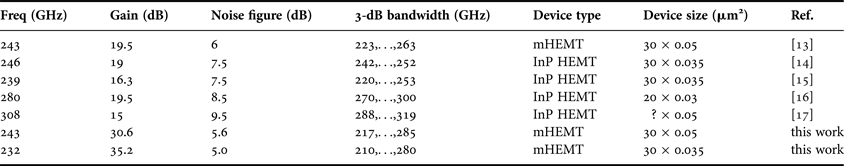
Table 2 shows a comparison of published results of WR-03 (220–325 GHz) low-noise amplifier modules. This overview is dominated by InP-based devices. By applying our metamorphic 50 and 35 nm HEMT technologies, we could successfully realize two very broadband LNA modules, demonstrating an excellent small-signal gain in combination with a state-of-the-art room temperature noise performance.
Table 2. Comparison of reported WR-03 low-noise amplifier modules*.
*Room temperature results.
VI. CONCLUSION
Two low-noise amplifier MMICs based on 50- and 35-nm metamorphic HEMT technology have been developed for operation in the high millimeter-wave frequency regime at 243 GHz and even beyond. To assemble the LNA circuits, a set of waveguide-to-microstrip transitions has been realized on 50-µm-thick GaAs substrates demonstrating an insertion loss of less than 0.5 dB between 210 and 300 GHz. The packaged 50 nm low-noise amplifier module achieved a small-signal gain of more than 28 dB between 218 and 280 GHz and a room temperature noise figure of 5.6 dB at 243 GHz. By applying the 35-nm mHEMT technology a second amplifier module was successfully fabricated, demonstrating a considerably improved small-signal gain, larger operation bandwidth as well as an excellent noise performance. The 35-nm H-band low-noise amplifier module achieved a linear gain of more than 32 dB between 210 and 280 GHz and a state-of–the-art noise figure of only 5.0 dB between 243 and 273 GHz. These results impressively demonstrate that advanced mHEMT technology is highly suitable for the realization of the next-generation active and passive millimeter-wave sensors.
ACKNOWLEDGEMENTS
The authors would like to thank their colleagues from the Fraunhofer IAF Epitaxy and Technology Department for excellent wafer growth and processing. This research was supported by the European Space Agency (ESA).
Axel Tessmann received the Dipl.-Ing. degree in Electrical Engineering from the University of Karlsruhe, Germany, in 1997 and the Ph.D. degree in Electrical Engineering from the University of Karlsruhe, Germany, in 2006. In 1997, he joined the High Frequency Devices and Circuits Department, Fraunhofer Institute for Applied Solid State Physics (IAF), Freiburg, Germany, where he is involved in the development of monolithically integrated circuits and subsystems for high-resolution imaging systems. His main research areas are the design and packaging of millimeter-wave and submillimeter-wave ICs using high electron mobility transistors on GaAs, GaN, and InP as well as circuit simulation and linear and nonlinear device modeling. He is currently Group Leader of the millimeter-wave packaging and subsystem group at the Fraunhofer IAF.
Volker Hurm was born in Schwäbisch Gmünd, Germany, in 1953. He studied Physics at the University of Tübingen and received the Diploma degree in 1979. In 1979 he joined the Fraunhofer Institute for Applied Solid State Physics in Freiburg where he worked initially on the modeling and characterization of silicon devices. He received his Doctor of Science degree from the University of Freiburg in 1983. Then he was engaged in the research and development of II/VI materials, the development of monolithic and hybrid integrated photoreceivers for up to 80 Gbit/s digital transmission systems, the design of 200 GHz GaAs Schottky diode frequency doublers, and the packaging of distributed amplifiers for 100 Gbit/s modulator driver operation. He is currently with the research division of High Frequency Devices and Circuits as a member of the scientific staff, where he is engaged in the development of MMICs and waveguide modules with operating frequencies up to 1 THz.
Arnulf Leuther received the Dipl. Phys. degree and the Ph.D. degree in Physics from the Technical University of Aachen. He is with the Fraunhofer Institute for Applied Solid State Physics (IAF), Freiburg, Germany, since 1996. The major working area is the development of HEMT technologies for sensor and communication systems up to 600 GHz.
Hermann Massler was born in Radolfzell, Germany, in 1965. He studied Electrical Engineering at the Technical University Karlsruhe, Germany, where he graduated in 1993. While working on his diploma degree at the Kernforschungszentrum Karlsruhe (KfK) he did quasi-optical measurements at 140 GHz. He continued these studies as Research Assistant in the KfK for one more year. Since 1994 he has been with the Fraunhofer Institute for Applied Solid State Physics (IAF) in Freiburg working on transistor- and IC-characterization up to 1.1 THz.
Rainer Weber was born in Offenburg, Germany, in 1978. He received the Dipl.-Ing. (FH) degree in Electrical Engineering from the University of Applied Sciences Offenburg, Germany, in 2003. He then joined the High Frequency Devices and Circuits Department of the Fraunhofer Institute for Applied Solid-State Physics (IAF), Freiburg, Germany, where he is involved in the MMIC design of amplifiers, oscillators, multipliers, and mixers up to 600 GHz.
Michael Kuri was born in Freiburg, Germany, in 1971. He received the diploma degree in Electrical Engineering from the University of Furtwangen, in 1996. From 1996 to 2000 he was with Storz, Kenzingen, Germany, where he was engaged in the design and routing of high-speed and high-frequency digital and analog circuits. In 2000, he joined the High Frequency Devices and Circuits Department, Fraunhofer Institute for Applied Solid State Physics (IAF), Freiburg, Germany, where he is involved in the design, measurement and packaging of analog and digital ICs.
Markus Riessle was born in Freiburg, Germany, in 1962. He received the certified engineer degree in Mechanical Engineering from the Gewerbeschule Freiburg, Germany, in 1994. From 1995 to 1999 he was with Raymond, Weil, Germany, where he was engaged in the design and layout of injection molding components for the automotive industry. In 2000, he joined the High Frequency Devices and Circuits Department, Fraunhofer Institute for Applied Solid State Physics (IAF), Freiburg, Germany, where he is involved in the packaging of millimeter-wave and submillimeter-wave modules and subsystems.
Hans-Peter Stulz was born in Lahr, Germany, in 1972. He received the certified engineer degree in Electrical Engineering from the Deutsche Angestellten Akademie, Karlsruhe, Germany, in 2002. From 1990 to 2009 he was with Marconi, Offenburg, Germany, where he was engaged in the characterization and optimization of linear and nonlinear circuits as well as radio link components and subsystems. In 2009, he joined the High Frequency Devices and Circuits Department, Fraunhofer Institute for Applied Solid State Physics (IAF), Freiburg, Germany, where he is involved in the packaging and characterization of millimeter-wave modules.
Martin Zink was born in Freiburg, Germany, in 1981. He received the certified engineer degree in mechanical engineering from the Deutsche Angestellten Akademie, Karlsruhe, Germany, in 2010. In 1999 he joined the Fraunhofer Institute for Applied Solid State Physics (Fraunhofer IAF), Freiburg, Germany, where he is involved in the computer-aided design and the microassembly of MMIC modules from 100 MHz to 1.1 THz.
Michael Schlechtweg received his Dipl.-Ing. degree in Electrical Engineering from the Technical University Darmstadt in 1982, and the Dr.-Ing. degree from the University of Kassel in 1989. He joined the Fraunhofer Institute for Applied Solid State Physics (IAF) in Freiburg, Germany, working on the design of millimeter-wave integrated circuits, and on nonlinear characterization and modeling of active RF devices. In 1994, he became head of the Simulation and Modeling Group at Fraunhofer IAF. Since 1996, he leads the High Frequency Devices and Circuits Department, focusing on the design and the characterization of devices and integrated circuits based on III–V compound semiconductors for RF applications, as well as the development of integrated circuits and modules for sensor and communication systems up to 500 GHz and above. Michael Schlechtweg received the Fraunhofer Prize in 1993, and the European Microwave Prize in 1998. He has co-authored about 200 scientific publications, and holds two patents.
Oliver Ambacher received his Dipl.-Phys. and Ph.D. degrees with honors from the Ludwig-Maximilians and Technical University Munich, in 1989 and 1993, respectively, where he was involved in the deposition and characterization of amorphous silicon for solar cells. In 1992, he received a German Science Foundation Graduate Research Fellowship. In 1993, he joined the Walter Schottky Institute of the TU-Munich to investigate the epitaxial growth of group-III nitrides based heterostructures. Since 1995 the research of his group is focused on fabrication of GaN based devices such as UV detectors, surface acoustic wave devices, or microwave amplifiers as well as on the understanding of polarization-induced effects in group-III nitride heterostructures and quantum wells. 1998/99, he spent 1 year at Cornell University, Ithaca, NY, as an Alexander von Humboldt fellow, where he was involved in the optimization of polarization-induced AlGaN/GaN HEMTs for high-frequency and high-power applications. He became a Professor of Nanotechnology and head of the Institute for Solid State Electronics located at the Technical University of Ilmenau in 2002. In 2004, he was elected as head of the new Center of Micro- and Nanotechnologies. Since 2007 he is the head of the Fraunhofer Institute of Applied Solid State Physics and Professor for Compound Microsystems in Freiburg, Germany.