I. INTRODUCTION
The radio frequency identification (RFID) systems have been rapidly growing technology over the decade, which uses RF signal for automatic identification of objects. RFID finds many applications in various areas such as agriculture, healthcare, airport, libraries, military, passport, supply chain, inventory, aircraft industry, mobile payment [Reference Xavier, Hikage, de Paula Pessoa and Fleury1], and smart parking application [Reference Pala and Inan2]. Several standards for RFID systems are currently in use (ISO, Class 0, Class 1 and Gen 2).
Globally, each country has its own frequency allocation for RFID. For example, RFID ultra high frequency (UHF) bands are: 866–869 MHz in Europe, 902–928 MHz in North and South America, and 950–956 MHz in Japan and some Asian countries. A typical passive RFID transponder called “tag” consists of an antenna and an application specific integrated circuit (ASIC) chip. These RFID tags can be active (with batteries), semi active or passive (battery less). A passive RFID system operates in the following way. A base station (reader) transmits a modulated signal with periods of unmodulated carrier signal, which is received by the passive tag antenna. The RF voltage induced on antenna terminals during unmodulated period is converted into dc. This induced voltage powers up the chip, which sends back the information by varying its front end complex RF input impedance. This impedance typically toggles between two different states, between conjugate match and some other impedance and as a result effectively modulating the back-scattered signal [Reference Seshagiri Rao and Nikitin3].
Several papers have been reported on RFID antennas including a tag antenna using meandered dipole and dual meandered dipole with reduced size [Reference Seshagiri Rao and Nikitin3–Reference Ma, Jiang, Xi and Ye6]. A RFID tag based on a planar inverted-F antenna is presented in [Reference Liu, Shen, Liu, Wu, Su and Liu7, Reference Hirvonen, Pursula, Jaakkola and Laukkanen8]. A dipole-based RFID tag antenna design consisting of folded dipole and ring structure at the end points has been observed to reduce the size of antenna [Reference Choi, Kim and Choi9–Reference Deleruyelle11]. Further, some tag antennas using slots on patch [Reference Deleruyelle and Pannier12–Reference Svanda and Polivka14] and miniaturized antenna design using patch [Reference Mirchandani, Deshpande and Khan15] have been discussed. Other tag antennas using meandered dipole with T-matched and inductive coupled feeding techniques [Reference Deleruyelle11, Reference Pumpoung, Wongsiritorn, Phongcharoenpanich and Kosulvit16–Reference Dhaoudi, Mabrouk, Vuong, De Souza and Ghazel23] have been reported for effective conjugate matching of input impedance. Double and triple split ring antenna topologies have also been reported to reduce the electric length of tag antenna [Reference Polivka, Holub, Vyhnalik and Svanda24], which further reduces the effective size of the antenna. Details on conjugate matching for RFID tag antenna is found in literature [Reference Marrocco25]. To increase the electrical length of the tag antenna, the meander line structure is utilized and method for calculating resonance frequency is detailed in literature [Reference Zhonghao and Cole26]. Out of the various techniques used for size reduction, dipole-based meandering size reduction and inductive coupled feeding techniques are reported to result better performances [Reference Deleruyelle11, Reference Pumpoung, Wongsiritorn, Phongcharoenpanich and Kosulvit16–Reference Dhaoudi, Mabrouk, Vuong, De Souza and Ghazel23].
The present work is focused on size reduction of RFID tag antenna for UHF band on low cost FR4 substrate. As a result, for the first time, the design of a smallest size (43 mm × 10 mm) antenna for UHF band on FR4 substrate is presented. The inductive coupled feed technique is used to improve the impedance matching and size reduction of the tag antenna. An EPC global class 1 Gen 2 Higgs 4 IC chip manufacturing by Alien Technology, USA [27] is used to design the proposed tag antennae with large resistor of 1.8 KΩ in parallel with a small valued capacitor of 0.95 pF. The circuit model of the RFID IC impedance is shown in Fig. 1.

Fig. 1. Circuit model of the RFID IC impedance.
The impedance of IC can be calculated at centre frequency 866 MHz of Indian RFID frequency band (865–867 MHz), which follows the European standard as:
 $$\eqalign{Z_{IC} = & R\;{\rm II}\;X_C \cr X_C = & \displaystyle{{ - j} \over {2\pi f_rC}} = \displaystyle{{ - j} \over {2\pi \times 866 \times 1.8 \times {10}^6 \times 0.95 \times {10}^{ - 12}}} \cr&= - j{\rm 193}.{\rm 45} \cr Z_{IC} = & {\rm 1}.{\rm 8}\;{\rm K}\Omega \;{\rm II} - j{\rm 193}.{\rm 45} \cr = & {\rm 2}0.{\rm 55} - j{\rm 191}.{\rm 45}\;\Omega.} $$
So the calculated impedance for Higgs 4 IC chip is 20.55 − j191.45 Ω.
II. CONJUGATE IMPEDANCE MATCHING METHOD
Let the effective power transmitted by the reader is EIRP R and the sensitivity is P c of the tag's transponder. P c is the minimum threshold RF power required by the chip to turn on and to perform back-scattering modulation. If there is a polarization matching between the reader and tag antennas, the maximum activation distance of the tag along the (θ, φ) direction is then given [Reference Seshagiri Rao and Nikitin3] by
 $$d_{max}(\theta, {\rm} \varphi ) = \displaystyle{c \over {4\pi f}}\sqrt {\displaystyle{{EIRP_R} \over {P_c}}\tau G_{tag}(\theta, \varphi )}, $$
where G tag (θ, φ) is the tag gain. The factor
 $$\tau = {\rm 1} - [\Gamma ]^2 = \displaystyle{{4R_cR_A} \over { \vert Z_{c +} Z_A \vert ^2}} \le {\rm 1,}$$
τ is the power transmission coefficient [Reference Seshagiri Rao and Nikitin3], where 0 ≤ τ ≤ 1 and Γ is the reflection coefficient, which accounts for the impedance mismatch between the antenna Z A = R A + jX A and chip impedance Z c = R c + jX c .
 $$\Gamma = \displaystyle{{Z_c - Z_A\;} \over {Z_c + Z_A}}.$$
The chip impedance depends on the input power, and frequency, since the transponder includes an energy-storage stage, so its input reactance is capacitive. As there is no direct 50 Ω transmission line so the antenna impedance should be inductive in order to achieve conjugate matching with chip impedance (20.55 − j191.45 Ω). Beyond d max , the power collected by the tag decreases below the microchip sensitivity, which further results the difficulty in detection of RFID tag. Figure 2 illustrates a passive RFID system operation.

Fig. 2. RFID System Operation. The backscattered signal is modulated by changes in chip impedance Z c .
In order to design a low-cost compact tag, an external matching networks involving lumped components is not a viable solution, therefore, the impedance matching network is proposed to build within the tag's antenna layout. Thereafter, the loop feeding technique based on inductive coupling is used to minimize the tag geometries.
III. ANTENNA DESIGN
The design schematic of the proposed meandered dipole antenna is shown in Fig. 3. The proposed meandered dipole antenna has three layers. The top metallic layer is the radiating element of thickness 30 µm is used to radiate the electromagnetic field, the middle layer is a low cost FR4 substrate with relative permittivity, ε r of 4.4 and tangential loss, tan δ of 0.02 and having thickness (h) of 1.6 mm, width W and length L and the bottom layer is ground layer having same dimension as that of substrate.

Fig. 3. Schematic of the proposed meandered dipole tag antenna.
The radiating element has several key parameters: “ma” is width of the meander, “ml” is height of the meander, ‘‘N’’ is number of meander used in antenna, “aw” is width strip line of antenna and “s” is the overall length of antenna as shown in Fig. 3(b).
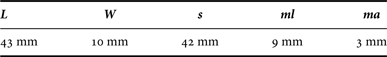
An initial design is to determine the size of the antenna to achieve intended tag size. So, initially, all the parameters of N = 2 × 3 meander line antenna are assumed, as presented in Table 1 and analyzed using approximate formulae given in [27].
Table 1. Assumed parameters of meander line antenna.
Based on the initially assumed value of the antenna parameters, the antenna was simulated using electro-magnetic simulator Ansoft HFSS v13. The impedance observed at 866 MHz is 2 + j1.5 Ω. This value is less than the desired impedance, which is needed to conjugate the chip impedance (20.55 − j191.45 Ω) at the same frequency. Thereafter, the width of meanders “ma”, and height of meanders “ml” are analyzed. It is observed from simulation results in Figs 4(a), 4(b), and 3(c) that antenna impedance increases by increasing these parameters for constant length (s) of meander line antenna.

Fig. 4. Variation of antenna impedance with frequency; (a) resistance as a function of meander width ma; (b) reactance as a function of meander width ma, and (c) reactance as a function of meander height ml.
Antenna resistance and reactance is controlled by changing the parameters of meander line antenna. From Fig. 4(c), the height of the meander ”ml” is studied by varying from 9 to 16 mm. The impedance of the antenna increases as “ml” increases. The suitable impedance with 7.28 + j195 Ω is chosen for “ml” is equal to 16.5 mm as imaginary part of this value is nearly equal to desired value. The return loss S 11 of −29 dB at 866 MHz for “ml” equals to 16.5 mm is observed as shown in Fig. 5 The resistance of the tag antenna is still relatively low and the size of antenna also increases with the increase of meanders height “ml” of antenna. Therefore, the inductive coupled loop technique is used to improve the impedance matching and size reduction of antenna.

Fig. 5. Simulated return loss of the proposed meandered dipole antenna at 866 MHz resonance frequency.
A) Antenna feeding using inductive coupled loop
The schematic of the proposed meander line antenna structure along with feeding loop arrangement is shown in Fig. 6. The antenna consists of a small rectangular loop for feeding and a meandered dipole, which are inductively coupled. The coupling is adjusted by the distance between the rectangular loop and the meandered dipole and the area of the loop. The inductive coupling is modeled by a transformer. The input impedance of the antenna in Fig. 6 is governed by equation (3):
 $$Z_{in} = Z_{loop} + \displaystyle{{{(2\pi fM)}^2} \over {\; Z_{md}}},$$
where Z loop = j2πf L loop and Z md are the individual impedances of the meandered dipole and rectangular loop for feed, respectively. M is the mutual inductance between them, as discussed in [Reference Sun, Xie and Cao22, Reference Polivka, Holub, Vyhnalik and Svanda24].

Fig. 6. Schematic of feeding loop of inductive coupled meander line antenna.
Independent of the condition that whether the dipole is at resonance or not, the total input reactance depends only on the loop inductance, L loop , while resistance is related to the transformer mutual inductance, M:
 $$\eqalign{R_{in}(\; f_o) = & \displaystyle{{{(2\pi f_oM)}^2} \over {\; R_A(f_o)}}, \cr X_{in}(\; f_o) = & 2\pi \ f_o\; L_{loop}.} $$
Therefore, input resistance and input reactance at the resonant frequency can be adjusted independently.
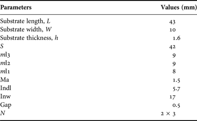
The geometry of the proposed inductive coupled meander line antenna is shown in Fig. 6. The length of antenna (s = 42 mm) is kept constant and the length of the meanders “ml1, ml2, and ml3” and meander width ma of the proposed meandered dipole antenna are determined by performing numerous parameter sweeps. To match the proposed meandered dipole antenna impedance Z A to the chip impedance Z c , inductive coupled loop feeding is used as shown in Fig. 7. Keeping meanders height ml3, ml2, ml1, and meander width “ma” and conductor spacing “s” constant, a parameter sweep is performed for “indl” and “inw”. When “indl” = 5.7 mm and “ind” = 17 mm the simulated results of impedance is 0 + j 98.6 Ω at 866 MHz, which is added to the impedance of radiating elements according to equations (3) and (4). The impedance is matched by varying the separation distance “gap” as shown in Fig. 8, between the radiating element and feed loop element from 0.5 to 1.5 mm.

Fig. 7. Geometry of proposed rectangular feed loop.

Fig. 8. Simulated model of inductive coupled meander line antenna.
The detailed and optimized parameters of Inductive coupled meandered line antenna shown in Fig. 16 is presented in Table 2.
Table 2. Optimized design specification of the proposed Inductive Coupled Meander Line Tag Antenna.
Figures 9 and 10 show the simulated input resistance and reactance, respectively, against UHF frequency of the proposed antenna with various separation distances, gap.

Fig. 9. Simulated input resistances as a function of frequency of the proposed inductive coupled meander line antenna with separation distances, gap.

Fig. 10. Simulated input reactance against UHF frequency of the proposed inductive coupled meander line antenna with various separation distances, gap.
It is clear that the input resistance and reactance can be increased or decreased by varying gap. Figure 11 shows the simulated return losses against UHF frequency of the proposed inductive coupled meander line antenna with various separation distances, gap.

Fig. 11. Simulated return losses against UHF frequency of the proposed inductive coupled meander line antenna with various separation distances, gap.
After examining parameter sweep results, it is observed that when gap = 0.5 mm, the antenna input resistance, R A is 27.9 Ω and input reactance, X A is 195.6 Ω. This shows that the proposed meandered dipole antenna input impedance is complex conjugately matched to the input impedance of the chip, i.e. R c is 20.55 Ω and X c is 191.45 Ω.
The variation of return loss of the proposed Inductive coupled meandered line antenna resonating at 866 MHz is shown in Fig. 12.

Fig. 12. Simulated return loss of the proposed inductive coupled meander line antenna at 866 MHz resonance frequency.
The minimum value of the simulated return loss [S 11] at the resonance frequency is −39.1 dB. The simulated −10 dB bandwidth of the proposed antenna is 134 MHz, from 748 to 882.3 MHz. With this bandwidth, the proposed tag antenna can be used in the UK and Europe UHF RFID systems.
The gain of the tag antenna is −16 dBi given in Fig. 13(a) considered at the center frequency of 866 MHz band (UHF RFID following frequency band standard of India). The radiation pattern of the proposed tag antenna is the omni-directional beam as shown in Fig. 13(b).

Fig. 13. Radiation pattern of Inductive coupled meander Line Antenna. (a) Radiation pattern of inductive coupled meander line antenna. (b) 3D polar gain of meander line antenna.
It is noticed that the antenna gain of inductive coupled meander line antenna is very less. This is due to the presence of ground and if the ground is removed from antenna design then gain of antenna increases as shown in Fig. 14, but the removal of ground causes deviation in the resonating frequency. So to achieve resonance at the same frequency, size of the antenna has to increase. Therefore there is a tradeoff between gain or size of antenna. The deviation of resonant frequency after removal of ground is shown in Fig. 15.

Fig. 14. Variation in gain of antenna by removing ground of antenna.

Fig. 15. Deviation in resonance frequency by removing ground of antenna.
Figure 14 presents the gain comparison between the antenna with ground and antenna without ground. When ground is removed from antenna the gain of antenna increases from −16.5 to −5 dB, but the resonant frequency gets shifted from 866 MHz to 1.31 GHz due to change in input impedance of antenna as shown in Fig. 15. So to get resonance frequency at 866 MHz the size of antenna has to be increased.
IV. FABRICATION AND MEASUREMENT
The prototype antenna is fabricated by using the designed parameters. The tags have size of 43 mm × 10 mm. The photograph of the proposed antenna is depicted in Fig. 16.

Fig. 16. Fabricated prototype inductive coupled meander line antenna.
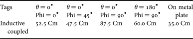
The maximum read range was measured by using integrated reader with the antenna gain of 9 dBi. Reading range of the tag at different orientations is given in Table 3. The maximum sensing reading range observed for the tag is nearly 87.5 Cm (max.) and decreases to 35 Cm (min.) when placed on metal platform/metallic housing.
Table 3. Reading range of Inductive coupled meander line antenna at different orientations.

In efforts to minimize the tag size, various design approach with their performance parameters has been tabulated as shown in Table 4.
Table 4. Various design approach with their performance parameters.

In view of the reported works, on the design and implementation of RFID tag for UHF band on FR4 substrate of thickness 1.6 mm, the overall antenna size (43 mm × 10 mm) in the present work is smallest among the tag antenna reported on FR4 substrate for UHF band applications. In the proposed design, the reduced antenna size is understood as a consequence of joint effect of increasing the permittivity and the presence of inductance line. The observed value of reading range varies from 87.5 to 35 Cms depending on mounting on non-metal and metal packages, respectively. The approach used for the design of compact tag, as presented above may also be tried on other flexible substrates for RFID identification of flexible packages.
V. CONCLUSION
In this paper, we have presented low cost compact antenna designing by two different methods. Both the antennae are designed for 865–867 MHz. The size of the antenna is 0.028λ × 0.12λ. The impedance matching is achieved by using Inductive coupled feed technique. The radiation pattern of the antenna is omni-directional beam. The effect of ground on gain and size of antenna are analyzed. The gain of antenna increases if the ground is removed but it shifts the resonance frequency. We measured the reading range at different orientations. The reading range of antenna in free space is nearly equal to 87.5 cm (max.) in free space and 35 cm (min.) on metal plate. Reading range of the tag is less because of the poor antenna gain and partially due to the large port gap (2 mm) of the antenna. The proposed tag having smallest size as reported before, particularly on the low cost FR4 substrate can be suitably used for short distance tagging applications in UHF band.
ACKNOWLEDGEMENTS
The authors want to thank the Wavelinx Technologies Pvt. Ltd., New Delhi, (India) for their kind support in experimental measurements. The work is financially supported by the World Bank assisted project TEQIP-II (subcomponent 1.1). Pvt. Ltd.
 Abhishek Choudhary received his B.Tech degree in 2013 and M.Tech. degree in Electronics and Communication Engineering from University Institute of Engineering and Technology, Kurukshetra University, Kurukshetra, India in 2015. His main research interests are RFID and antennas.
 Krishan Gopal received his Bachelor of Technology from Kurukshetra University, Kurukshetra, Haryana, India in 2007, and received Masters of Engineering from Thapar University, Patiala, Punjab, India in 2010. He is currently working as Assistant Professor and pursuing Ph.D. Degree in the department of Electronics and Communication Engineering from University Institute of Engineering and Technology, Kurukshetra University, Kurukshetra, Haryana, India. His areas of interest include Microwaves, Microstrip Antennas and filters, Wireless communications. He published five papers in various Journals.
 Deepak Sood received his B.Tech (ECE) degree in 2002 and M.Tech (ECE) in 2007. He is currently pursuing his P.hD from UIET, Kurukshetra University, Kurukshetra. He is currently working as an Assistant professor in the Department of Electronics & Communication Engineering of UIET, Kurukshetra University, Kurukshetra (Haryana), India. He has more than 25 research papers at national and international level in various fields of RF engineering. His research interests include design and development of Metamaterial-based microwave absorbers for millimeter and THz range, Frequency selective surface development, Microstrip Antenna design, Planar integrated waveguide design & development. He is a reviewer of various journals.
 Dr. Chandra Charu Tripathi received his B.Sc.(Honors) Physics) and M.Sc. (Solid State Electronics Devices) degrees from Bannaras Hindu University, Varanasi, India in 1985 and 1987, respectively, followed by Master in Engineering (Microelectronics) from BITS, Pilani, India in 1991. He worked at IDDC – a R&D center of Haryana State Electronics Development Corporation (HARTRON) from 1991 to 2003. He received his Ph.D. in Electronics from Kurukshetra University, Kurukshetra, India in the year 2009 and serving as a professor in Kurukshetra University. His research interests include optoelectronics products, optical networks, Optical devices, optical fiber communications, sensor networks, MANETS, microwave propagation, antenna, VLSI devices/ technology Bio-MEMS/RF MEMS devices. He has supervised more than 30 M.Sc. and M. Tech. students, and presently supervising seven numbers of Ph.D. students. He has more than 25 papers in refereed journals and 40 in national/international conferences. He is a semiconductor technologist and a reviewer for many journals.