Introduction
Ultra-wideband (UWB) antennas are more and more appreciated in the recent years after determining 3.1–10.6 GHz by the US Federal Communications Commission (FCC) [1]. In [Reference Li and Luk2], a differential-fed technique is used to design UWB antenna with unidirectional radiation patterns. In [Reference Kang, Shi and Liang3], a new substrate-integrated magneto-electric dipole antenna is presented for UWB applications. In [Reference Qu, Chan and Xue4], a composite cavity-backed folded structure is proposed to design a bowtie UWB antenna. Wide bandwidth (BW) is one of main features of the UWB antennas [Reference Yeboah-Akowuah, Kosmas and Chen5–Reference Mighani, Akbari and Felegari10]. In [Reference Emadian, Mirmozafari, Ghobadi and Nourinia11], two L-shaped stubs on the back side of the substrate are introduced for BW enhancement. In [Reference Emadian and Ahmadi-shokouh12], two semi-circle slots in the ground plane are employed to enhance the BW up to 23 GHz. In [Reference Naser and Dib13], to improve the impedance BW, a notch is cut from the ground plane and the edges of the radiation patch are chamfered with specific dimensions. In [Reference Ojaroudi, Ojaroudi and Ojaroudi14], by cutting two pairs of U-shaped slots in the ground plane, additional (third and fourth) resonances at 11 and 14 GHz are excited and much wider impedance BW can be produced. However, this ultra-wide frequency range of UWB systems leads to interference with narrow band wireless communication systems like Wireless Local Area Network (WLAN) that works on frequencies of 5.15–5.35 and 5.725–5.825 GHz as well as X-band working on frequencies of 7.25–7.75 GHz for satellite applications. Hence, an especial UWB antenna is required to remove interfering bands.
There are many methods to remove interfering bands such as using slot in the ground plane and main patch of the antenna [Reference Abazari Aghdam15–Reference HU, Chen, Law, Shen, Zui, Zhang and Due17] and adding resonators on the ground plane or main patch of the antenna [Reference Sarkar, Srivastava and Saurav18, Reference Siddiqui and Antar19]. In [Reference Emadian and Ahmadi-shokouh20], a T-shaped and a pair of L-shaped stubs are added to UWB antenna structure to reject WiMAX and WLAN spectrum. In [Reference Bahmani, Mazloum and Ojaroudi21], an inverted X-shaped slot and a pair of coupled C-shaped parasitic structures are employed to achieve band-notched characteristics. In [Reference Emadian, Ahmadi-shokouh, Raeesi, Askani and Nazari22], by employing an inverted T-shaped stub connected to the ground plane and two U-shaped and Ω-shaped slots in the modified patch, triple band-notched properties are obtained. In most recently reported articles, only frequency characteristics of UWB antennas are investigated.
In impulse radio (IR) UWB systems, UWB antennas should be able to transmit and receive extremely narrow pulses. Therefore, the time-domain performance of an UWB antenna should be considered in designing process. This paper presents a new UWB antenna with dual band-notched characteristics. By adding two L-shaped stubs to the narrow rectangular radiation patch, the first notched band in WLAN spectrum is obtained. The second notched band in X-band spectrum is achieved using narrow straight strip placed on the back side of the substrate. Two small parasitic strips are also connected to the narrow rectangular radiation patch to enhance the impedance BW of the antenna. The effect of the proposed antenna structure on transmitting and receiving of different UWB pulses such as Rayleigh, modulated Gaussian (MG), and square root raised cosine (SRRC) pulses in different scenarios is fully investigated. The results are compared in term of system fidelity factor (SFF), which is the similarity factor between different signals. Moreover, the impulse response of the proposed antenna system in indoor propagation channel is fully investigated. A sub-band divided ray-tracing (RT) approach is applied to simulate indoor channel characteristics. Also, a frequency-domain measurement setup is applied to measure the impulse response of the proposed antenna system in an anechoic chamber and indoor environment. Table 1 compares several recently reported UWB antennas with the proposed dual band-notched UWB antenna. As seen from the table, the proposed antenna has a compact and small size with very wide operation BW from 2.7 up to 14 GHz. The gain of the proposed antennas varies from 0.5 to 3.5 dB over the frequency BW. The low gain values of the proposed antenna at low frequencies are due to the relatively small electrical size of the antenna at these frequencies.
Table 1. Comparison of different recently reported UWB antennas

Antenna structure
The geometry and structure of the proposed antenna is shown in Fig. 1. The antenna is realized on FR4 sub-layer with aspects of 20 mm × 20 mm, thickness of 0.8 mm, and relative dielectric constant of 4.4. A large slot with a size of 19 mm × 12 mm is created as a radiation slot in the ground plane. The proposed antenna includes a simple narrow rectangular patch connecting to a 50 Ω microstrip feed line, the feed line dimensions are 1.35 mm × 5.2 mm. As shown in Fig. 1, two small parasitic strips with given values are connected to the radiation patch and a small rectangular slot with dimensions of 1.6 mm × 4 mm is etched out from the ground plane. Two L-shaped stubs with a horizontal arm of 5.4 mm and a vertical arm of 5 mm are positioned alongside the antenna rectangular radiation patch. Finally, a rectangular backed plane stub with a length of 11 mm and a width of 0.2 mm is added to the antenna structure.

Fig. 1. Geometry of proposed antenna (units: millimeters).
Design procedure and frequency-domain characteristics
ANSYS-HFSS 15 based on the finite element method is applied to optimize and simulate the proposed antenna in frequency domain. Figure 2 demonstrates the design steps of the dual band-notched UWB slot antenna, and the simulated S 11 curves corresponding to these steps are shown in Fig. 3. In the first step, a simple rectangular microstrip line and a rectangular slot with proper size in the ground plane are applied to excite the dominant mode at lower frequencies as shown in Fig. 3. A small rectangular slot is etched out from the ground plane just below the microstrip line for better impedance matching. In the next step, two L-shaped stubs are added to the rectangular patch to obtain band-notched property in WLAN spectrum. As seen from Fig. 3 in this step, the impedance matching of the antenna is also improved especially at middle frequencies of the band (6–11 GHz).

Fig. 2. Proposed antenna designing steps.

Fig. 3. Simulated S 11 of different steps shown in Fig. 2.
This is due to the fact that more electrical current paths and resonance features are created using these L-shaped stubs. At notch frequencies, the antenna works in transmission line-like mode.
At first notch frequency (5.5 GHz), the two L-shaped stubs act as quarter wavelength resonator, and as shown in the next section, the surface currents on these stubs and narrow rectangular radiation patch are in opposite direction, and therefore they neutralize the effects of each other, and hence band-notched characteristics can be achieved.
In step 3, a narrow rectangular stub is positioned on the rear side of the antenna to reject X-band spectrum. This stub acts as half a wavelength resonator at 7.5 GHz. At this frequency, the surface currents are highly concentrated on the straight stub backed plane and are in opposite direction with those on the rectangular radiation patch leading to band-notched properties in X-band downlink satellite systems. Finally, in step 4, two parasitic strips are added to the radiation patch to further enhance the antenna BW. In fact, the coupling between the radiation patch and the rectangular radiation slot can be tuned by using these parasitic stubs. As shown in Fig. 3, a new resonance around 13 GHz can be created in step 4. Figure 4 shows the simulated and measured S 11 (return loss) of the proposed antenna. The photo of the fabricated antenna is also shown in the figure. The results are in good agreement and the proposed antenna has very wide impedance BW from 2.7 up to 14 GHz with dual band-notched characteristics in WLAN and X-band spectrums. Figure 5 shows the gain of the proposed antenna. The antenna gain is low at lower frequencies. It can be due to the small size of the antenna, but the gain increases as the frequency increases, because at higher frequencies, the radiation patterns of the antenna are somewhat directed. It can clearly be seen that there are two nulls in the gain diagram at around 5.5 and 7.5 GHz. These nulls occur due to the performance of the L-shaped stubs and straight conductor backed plane in WLAN and X-band. The filtering structures have no effects on the other frequencies, and the gain is almost constant over the UWB band as shown in Fig. 5.

Fig. 4. Measured and simulated S 11 of the proposed antenna.
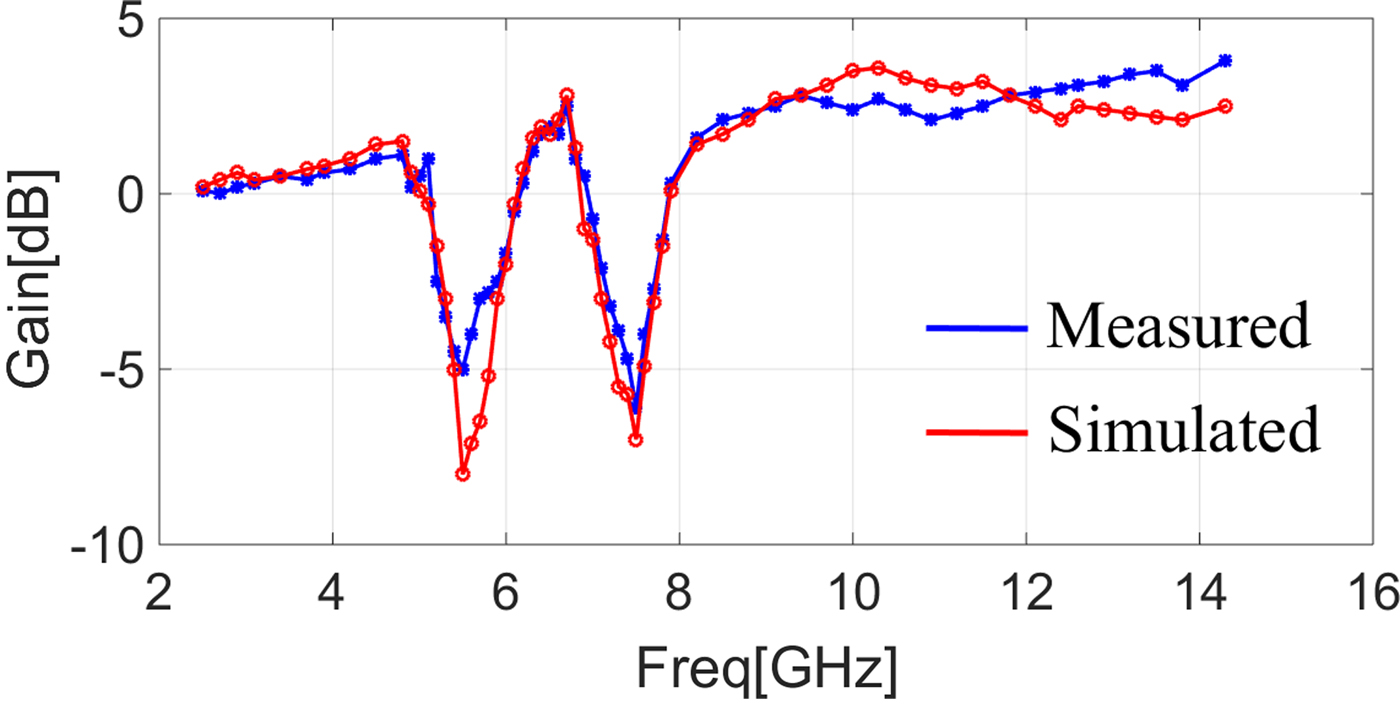
Fig. 5. Measured and simulated gain of the proposed antenna.
Figure 6 shows the radiation patterns of the proposed antenna in two cut planes: H-plane (X–Z) and E-plane (Y–Z). It can be seen that the proposed antenna has omnidirectional radiation patterns in the X–Z plane and dipole-like radiation patterns in the Y–Z plane. The radiation patterns have more distortions at higher frequencies compared with lower frequencies, it could be due to the excitation of higher modes at higher frequencies.

Fig. 6. Measured radiation patterns of the proposed antenna at (a) 4, (b) 6.5, and (c) 9.5 GHz.
Conceptual equivalent circuit model of proposed antenna
To better understand the dual band-notched characteristics, first the current distribution of the proposed antenna at different notched bands is illustrated as shown in Fig. 7. Figure 7(a) demonstrates the simulated current distribution at the first notch frequency (5.5 GHz) related to the WLAN band and Fig. 7(b) illustrates the current distribution at the second notch frequency (7.5 GHz) related to the X-band. It is observed that the surface current is more concentrated on the L-shaped stubs at 5.5 GHz and more concentrated on the backed plane straight resonator at 7.5 GHz. At notched frequencies, the surface currents on the main patch and filtering structures are in opposite direction as shown in Fig. 7 with dashed lines; therefore, they neutralize the resultant fields of each other, which lead to the band rejection properties at 5.5 and 7.5 GHz.
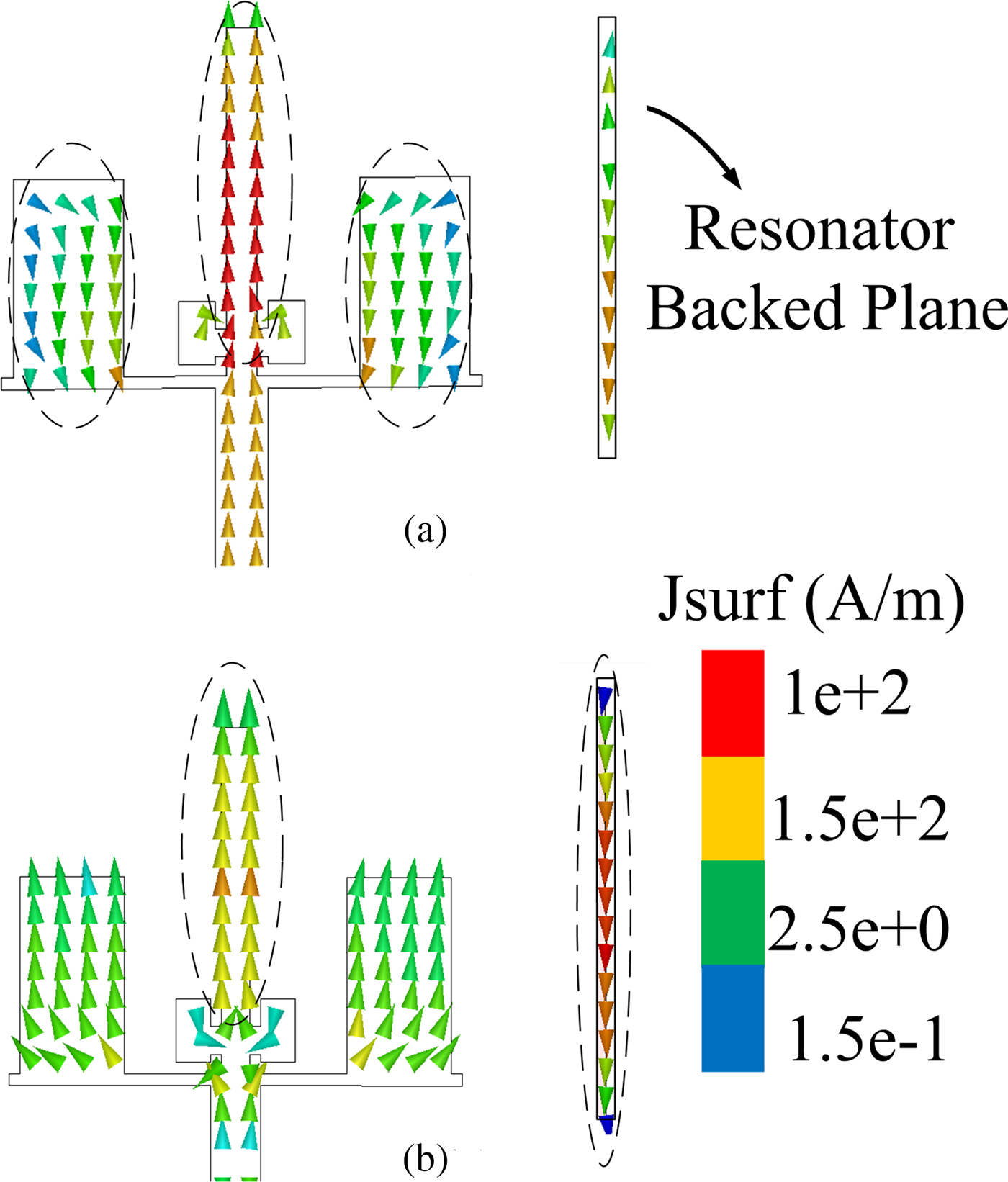
Fig. 7. Simulated current distribution of the proposed antenna at (a) 5.5 and (b) 7.5 GHz.
In this section, a lumped element equivalent circuit model is applied to provide an accurate explanation for the input impedance of the proposed antenna. It is noted that the input impedance of the proposed dual band-notched antenna is equivalent to the input impedance Z a of the reference UWB antenna without band-notched structures (L-shaped and straight stubs) connected with series and/or parallel resonant circuits at the center frequencies of the notched bands. If a UWB antenna is well matched, it can be modeled as a 50 Ω load. Figure 8 shows the simulated and measured input impedance of the proposed antenna. From the simulated or measured input impedance data, it is evident that the resistance is about 50 Ω and the reactance is close to zero over the UWB BW except at the notched bands. In WLAN band, the input resistance is low about 20 Ω at 5.2 GHz, while it is very high about 300 Ω at 5.6 GHz; while the reactance curves are varying from negative to positive and positive to negative values, respectively. It demonstrates a parallel resonance properties around 5.2 GHz and a series resonance properties about 5.6 GHz. Similarly, in X-band, the resistance is high about 120 Ω at 7.4 GHz and relatively low about 29 Ω at 7.8 GHz, while the reactance curves are varying from positive to negative section and negative to positive section indicating parallel and series resonance properties, respectively.

Fig. 8. Input impedance of the proposed antenna: (a) resistance and (b) reactance.
According to the above illustrations, the band-notched structures can be modeled by RLC resonant components as shown in Fig. 9. To determine the parallel and series RLC components (R pn, C pn, L pn, R sn, C sn, L sn, where n = 1,2) the BW of the corresponding notched band should be determined. For a parallel RLC resonant circuit, BW is the limit where the resistance is equal to or higher than 0.707 of the peak value. It can be determined from the results shown in Fig. 8. The RLC components of a parallel resonant circuit can be obtained as follows: [Reference Gheethan and Anagnostou23]
 $$BW_p = \displaystyle{1 \over {R_PC_p}},$$
 $$f_{0p} = \displaystyle{1 \over {2\pi \sqrt {L_pC_p}}}, $$
where R p, L p, and C p are the resistance, inductance, and capacitance of the parallel resonant circuit, respectively, and f 0p is the center frequency of the band related to the parallel resonant feature. For a series RLC resonant circuit, BW is the range where the resistance is equal to or lower than 1/0.707 of the minimum value. The RLC components of a series resonant circuit can be achieved using following equations:
 $$BW_s = \displaystyle{{R_s} \over {L_s}},$$
 $$f_{0s} = \displaystyle{1 \over {2\pi \sqrt {L_sC_s}}}, $$
Fig. 9. Lumped element equivalent circuit model of the proposed antenna.
where R s, L s, and C s are the resistance, inductance, and capacitance of the series resonant circuit, respectively, and f 0s is the center frequency of the band related to the series resonant property. The approximate values of the lumped elements of the parallel and series RLC circuits are determined initially using above equations. Afterwards, the lumped element equivalent circuit model is adjusted and optimized using ADS 2016 software package.
The input impedance properties of the equivalent circuit model are also shown in Fig. 8 and compared with those obtained from the measurement and HFSS simulation of the proposed antenna. It can be seen that the results are in good agreement. The discrepancy is mainly because of the inaccurate modeling of the UWB antenna. The calculated and optimized values of RLC components obtained by ADS are given in Table 2.
Table 2. Optimum values of lumped elements in equivalent circuit model

Antenna characteristics in time domain
CST Microwave Studio software based on a time-domain finite integration technique is applied to investigate the time-domain performance of the proposed antenna. The antenna system considered for time-domain analysis includes two identical proposed dual band-notched monopole antennas separated with a distance of 50 cm from each other in the face-to-face and the side-by-side scenarios. A frequency-domain measurement setup is used to measure the antenna system transfer function in the anechoic chamber. Thereafter, the impulse response of the proposed antenna system can be obtained from the transfer function by applying inverse fast Fourier transform. As indicated in [Reference Koohestani, Zürcher, Moreira and Skrivervik24], frequency-domain measurements have the advantage of ability to describe different excitation signals. This method is free from ambiguity. Different pulses to be transmitted are defined in Matlab, and then by applying a fast Fourier transform, their frequency response can be achieved. By multiplying these data with the transfer function of the antenna system, the frequency response of the received signals can be achieved. Finally, using the inverse Fourier transform, the received signals in time domain are obtained. In this case, the measurements are performed in the anechoic chamber in order to achieve only the antenna effects and eliminate the multipath effects of the surrounding environment. Before analyzing the time-domain performance, the phase of transfer function of the antenna system (phase of S 21) is simulated and measured for both the scenarios and shown in Fig. 10. It can clearly be seen that the phase is almost linear over the entire UWB band, which is suitable to achieve constant group delay for sending and receiving of ultra-short pulses without distortion. As shown in Fig. 10, two phase distortions occur at the two notch frequencies because of the filtering structures in the antenna geometry leading to the pulse shape distortion at these frequencies. Figure 11 shows the group delay of the proposed antenna in face-to-face and side-by-side cases. It is observed that the group delay is chiefly constant over the desired BW except at two notch frequencies.
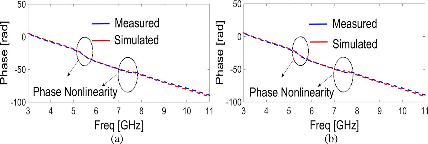
Fig. 10. Phase of the proposed antenna system in (a) face-to-face and (b) side-by-side scenarios.
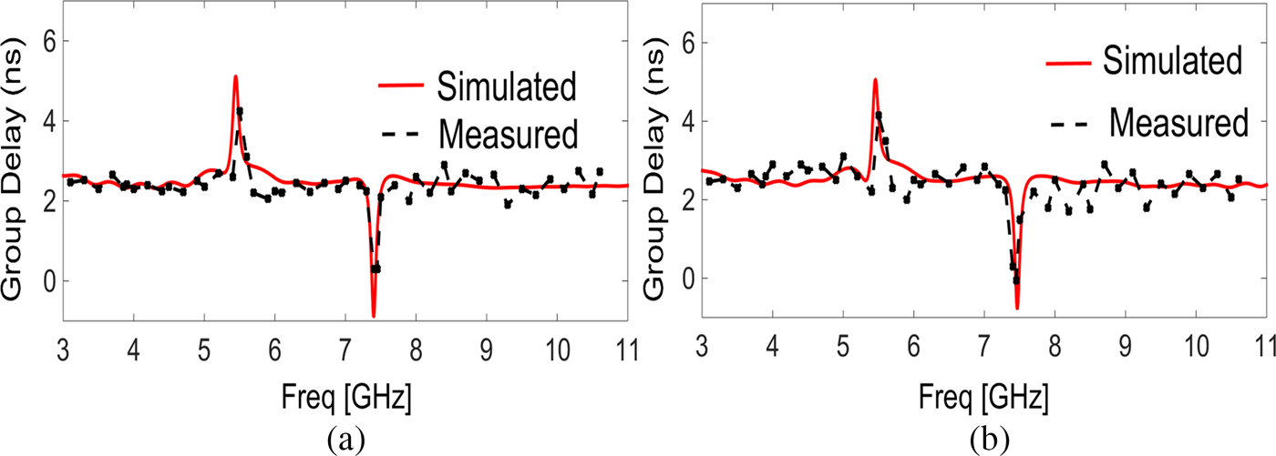
Fig. 11. Group delay of the proposed antenna system in (a) face-to-face and (b) side-by-side scenarios.
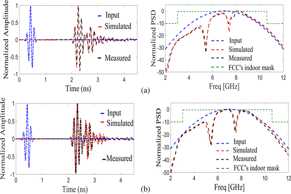
The group delay highly varies at notch frequencies. It can be described by the results shown in Fig. 10 where the phase non-linearities and band-notched characteristics occur at these frequencies. Because of the above-mentioned advantage of describing different input signals, in this paper, Rayleigh, MG, and SRRC pulses are applied as excitation signals and different received pulses are compared in term of SFF. These signals BW is between 3 and 11 GHz. Figures 12–14 demonstrate the input and received different signals and their power spectral densities (PSDs) in dB for both face-to-face and side-by-side cases. The FCC indoor mask is also shown in these figures for comparison. It is seen that the PSDs of the received MG and SRRC signals fully comply with power spectrum-limited mask defined by FCC, while the PSD of the received Rayleigh pulse does not agree well with the limited mask, especially at lower frequencies. The received signals experience few ripples and fluctuations in its duration time due to the antenna structure and band-notched characteristics. Two sharp decreases occur in their PSD diagram at the two notch frequencies indicating that the part of the input signals that covers these frequency bands is distorted and the antenna cannot radiate effectively; therefore, band-notched characteristics can be achieved at these frequencies. To evaluate different received signals in both the scenarios, the SFF [Reference Quintero, Zürcher and Skrivervik25], which describes the correlation between the input and received signals, is computed and its values are tabulated in Table 3. The SFF changes between 0 and 100%. A SFF value of 100% demonstrates that the received signal is fully matched with the input signal, while a value of 0 shows that the received signal is fully different than the input signal. A distortion higher than 50% can cause the pulse approximately unrecognizable [Reference Quintero, Zürcher and Skrivervik25]. It is seen from Table 3 that the similar results are obtained in the face-to-face and the side-by-side scenarios showing again that the proposed antenna radiates omnidirectionally. The obtained SFF values for MG pulses are more than those of Rayleigh and SRRC pulses. It is because of the wider BW and high-level power of Rayleigh and SRRC pulses under the influence of more filtering effects of the proposed antenna. However, for different pulses and scenarios, the results show that the SFF values are quite acceptable (>50%) for UWB impulse communication [Reference Quintero, Zürcher and Skrivervik25].

Fig. 12. Input and received Rayleigh signals and their PSD (dB) in (a) face-to-face and (b) side-by-side scenarios.

Fig. 13. Input and received MG signals and their PSD in (a) face to face and (b) side by side scenario.

Fig. 14. Input and received SRRC signals and their PSD in (a) face to face and (b) side by side scenario.
Table 3. SFF values of proposed antenna system for different pulses in different scenarios

Indoor propagation channel characteristics
Because of low-power constraint of UWB systems, which is determined by FCC, these systems are applied chiefly in indoor environments. Therefore, in designing of such systems, investigations and analyses on indoor propagation channels should be performed. In this section, the indoor propagation channel characteristics of the proposed antenna in a typically indoor office will be analyzed. An RT approach based on the geometrical optics and uniform theory of diffraction is applied to simulate the impulse response of the UWB propagation channel. The conventional RT methods can only be used for narrow band systems where the antenna radiation characteristics and electrical properties of materials are assumed constant over the desiring frequency BW. However, UWB systems do not follow the narrowband assumptions. This method requires to be changed for UWB applications. In our study, a sub-band divided RT approach is applied to cover the channel characteristics over the UWB BW. The steps of a sub-band divided RT method is shown in Fig. 15.

Fig. 15. Steps of sub-band divided ray tracing method.
These steps are as follows:
(1) The total BW is divided into several sub-bands, each of which should be narrow enough for assuming same frequency characteristics.
(2) The traditional RT method is used to obtain the corresponding delay profiles at the center frequency of each sub-band.
(3) Afterwards, the Fourier transform is used for achieving the channel transfer function at each sub-band; the accurate parts are extracted and combined together to obtain a new frequency response for the entire BW.
(4) Ultimately, the frequency responses are transformed back to the time domain applying an inverse Fourier transform to obtain a delay profile that is valid for the entire BW.
The total BW is divided to 15 sub-bands. The channel impulse responses (CIRs) at each sub-band are achieved by considering the propagation phenomena (reflections, diffractions, and refractions). At each sub-band, the simulated frequency-dependent radiation patterns of the proposed antenna is incorporated in the RT model. It can be easily done since in the RT approach the angle of arrival and the angle of departure are given. Also at each sub-band, the electrical characteristics of the environment materials derived from the literature [Reference Safaai-Jazi, Riad, Muqaibel and Bayram26] are inserted in the RT model. The realistic indoor environment selected for simulation and measurement is shown in Fig. 16. It consists of a room with four walls, a ceiling and floor constructed from the concrete, a glass window, wooden door, and wooden shelves. A wooden table and a comfortable chair are placed at the left side of the room as well as an office desk with an armchair are positioned in the room as shown in Fig. 16. The constructed three-dimensional RT model is also shown in Fig. 16. The overall size of the room is 4.7 m × 5.2 m × 2.8 m. In order to achieve an accurate model for realistic indoor propagation channel, the simulations and measurements should be computed for a large amount of points. A grid of receivers with 10 × 10 points are placed over the same 10 cm × 10 cm area on the table with 1 cm resolution. The transmitter is placed at the right side of the room below the shelves with a distance of 2.85 m from the center point of the receivers. The height of the transmitter and receiver is the same in order to avoid polarization mismatch loss. For truncating the simulation time, in the RT model, only the rays with one diffraction and three reflections or less are considered, because the higher order reflected or diffracted rays have no significant energy and can be ignored. Figure 17 demonstrates the CIR of the proposed scenario (indoor UWB channel) at the center point of receivers when the two proposed antennas are applied as transmitter and receiver antennas. The power of transmitter and noise floor are 10 and −90 dBm, respectively. For the better view, the CIRs of the sub-bands numbered by 1, 5, 7, 9, and 12 are only shown. We know from Friis formula that signals experience more free space loss at high frequencies compared with the low frequencies. However, because of higher gain values of proposed antennas at higher frequencies, it is seen from Fig. 17, comparing the first received impulses (line of sight ray) at different sub-bands, the signal amplitudes are almost fixed except at notched sub-bands. At notch frequencies (sub-bands 5 and 10), because of the band-notched properties of the proposed antenna, the amplitude and number of multipath components are very low as desired. A frequency measurement setup is used to measure CIRs and power delay profile (PDP) of the proposed scenario. Because of the Fourier transform relation between the channel's impulse response and transfer function, it is possible to achieve the CIR by measuring the channel transfer function (S 21). This method is to be accurate like many time domain approaches when time-variant channel and long distance are not taken into account [Reference Ghassemzadeh, Jana, Rice, Turin and Tarokh27].
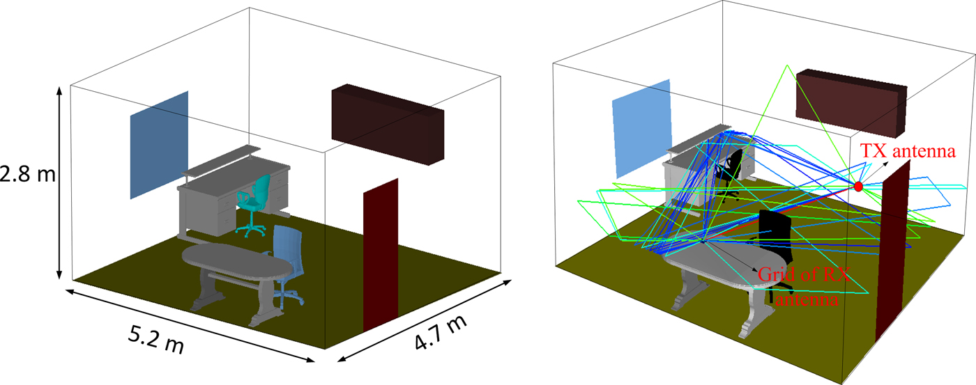
Fig. 16. Geometry of indoor propagation channel and ray tracing reconstruction model.
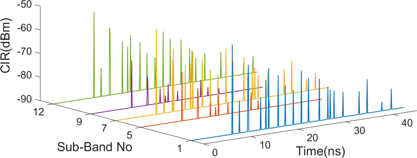
Fig. 17. Channel impulse response of different sub-bands.
A vector network analyzer (VNA) is applied to measure the magnitude and phase of the channel transfer functions by connecting two proposed antennas to the ports of the VNA in the proposed indoor channel. Afterwards, the CIR can be achieved using the inverse Fourier transform method. The TX antenna is fixed while the RX antenna is moved on the grid mentioned earlier through the rail controlled by a laptop. The transmitted power is 10 dBm and the noise floor is −90 dBm.
The frequency measurements are preformed over the UWB frequency range (3.1–10.6 GHz) with a frequency step of Δf = 4.86 GHz leading to 1601 frequency samples. From this frequency sample interval of 4.68 MHz, a time response about 200 ns duration is achieved by inverse Fourier transform option. Several multipath properties such as average delay, RMS delay spread, and maximum excess delay can be achieved from PDP. The PDP is the power of a signal received at the receiver through a propagation channel as a function of time delay. The PDP is achieved from averaging the square values of the normalized CIRs obtained over all the grid points and removing the propagation delay. Figure 18 demonstrates the PDP extracted from the sub-band divided RT method and measurement data. A good agreement between simulation and measurement results is achieved. The small difference between results is because of the approximation of material electrical properties used from the literature, the high-order propagation mechanism (reflection, diffraction, and refraction) which are not considered by the RT model, and the angular spatial resolution which determines the direction of launched rays in the RT model. The angular spatial resolution selected in our RT model is 1°. The lower values of angular spatial resolution lead to more precision. Moreover, the number of sub-bands is an important parameter on accuracy of simulation results. By increasing the number of sub-bands, more accurate results can be achieved but the computational time increases greatly.

Fig. 18. Simulated and measured power delay profile of indoor propagation channel.
Conclusion
In this paper, a novel compact UWB slot antenna with a size of 20 mm × 20 mm is introduced. The proposed antenna has a wide BW ranging from 2.7 up to 14 GHz and two notched bands in WLAN and X-band. By adding a pair of L-shaped stubs to the main rectangular patch, the first band-notched property in the 5–6 GHz band (WLAN band) can be achieved. Moreover, by employing these stubs, impedance matching of the antenna is highly improved specially at middle frequencies of the band. The second band-notched characteristic is obtained in the 7–8 GHz band (X-band) by inserting the straight resonator printed on the back side of the substrate. Finally, a pair of small parasitic strips are connected to the main patch to further enhance the BW of the antenna. In order to show the mechanism of the proposed antenna, a lumped element equivalent circuit model is presented and studied. The proposed antenna shows satisfying radiation characteristics in both the H-plane and the E-plane. The time-domain performance of the proposed antenna in the face–to-face and the side-by-side scenarios with different excitation pulses is also investigated in detail. The results show that the proposed antenna is a suitable candidate for UWB IR applications. Moreover, the indoor CIR of the proposed antenna in the simple office room is fully investigated and the simulated and measured results are compared.
 Seyed Ramin Emadian received the B.Sc. degree in electrical engineering from the University of Mashad, Mashad, Iran, in 2008, the M.Sc. degree in electrical engineering from the University of Urmie, Urmie, Iran, in 2011. He is currently working toward the Ph.D. degree at the University of Sistan and Baluchestan, Zahedan, Iran. From 2013, he is with the Department of Electrical Engineering, University of Sistan and Baluchestan. His research concerns include millimeter-wave and ultra-wideband systems, analysis and design of multi band microstrip antennas, circular polarization patch antennas, multiple input and multiple output antennas, and multi band-notched UWB antennas.
 Javad Ahmadi-Shokouh received the B.Sc. degree in electrical engineering from Ferdowsi University of Mashhad, Mashhad, Iran, in 1993, the M.Sc. degree in electrical engineering from the University of Tehran, Tehran, Iran, in 1995, and the Ph.D. degree in electrical engineering from the University of Waterloo, Waterloo, ON, Canada, in 2008. From 1998 to 2003, he was with the Department of Electrical Engineering, University of Sistan and Baluchestan, Zahedan, Iran, as a Lecturer, where he is currently an Assistant Professor. He was also with the Department of Electrical Engineering University of Manitoba, Winnipeg, MB, Canada (2008–2009) as a Postdoctoral Fellow. His research interests are antenna and microwave systems for all applications, millimeter-wave and ultra-wideband systems, smart antennas, and optimal and adaptive MIMO systems.