I. INTRODUCTION
In the recent years, two frequency spectrums, the unlicensed 60 GHz and the sparsely licensed E-band, have increased in significance due to advancement in point-to-point wireless communications. Multi-gigabit communication systems using these frequencies bands can outperform their optical fiber counterparts and will likely become the industry standard [Reference Dyadyuk1]. In general, millimeter-wave systems have much smaller device footprints and allow wider bandwidths.
It is well known that radio frequency micro-electro-mechanical system (RF MEMS) devices offer attractive characteristics in microwave frequencies. They also exhibit similar advantages in millimeter-wave spectrum in terms of high isolation, low insertion loss, low DC power consumption, and excellent linearity [Reference Rebeiz2]. In [Reference Grant, Denhoff and Mansour3], RF MEMS switches have been comprehensively compared with semiconductor switches and have shown to be optimal for millimeter-wave applications.
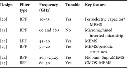
Bandpass filters are the critical components in modern communication systems. Reconfigurable or tunable microwave filters will be even more indispensable as multi-channel systems are becoming possible. Several different types of RF MEMS tunable filters emerged in the past decade and different frequency bands use and capability became possible [Reference Chan, Foulardi, Ramer and Mansour4–Reference Ou and Rebeiz11]. Some of the challenges in microwave tunable filters have already been tackled. Many tunable designs focused on using lower frequency and high-Q bandpass filters [Reference Fouladi, Huang, Yan and Mansour12–Reference Cheng and Rebeiz16]. Other research groups developed techniques for tunable bandpass filters with bandwidth control [Reference El-Tanani and Rebeiz17–Reference Naglich, Lee, Peroulis and Chappell19]. Different technologies and techniques have been offered, including ferroelectric capacitors, RF MEMS, superconducting MEMS, and complementary metal-oxide-semiconductor (CMOS) MEMS, all in the millimeter-wave domain [Reference Lugo, Wang, Papapolymerou, Zhao, Wang and Hunt20–Reference Hsieh, Chen, Lin and Chang25].The key features of these designs are summarized in Table 1.
Table 1. Previous work: millimeter-wave MEMS and micro-machined filters.

BPF, bandpass filter; LPF, lowpass filter; BSF, bandstop filter.
However, up to date, only a limited work has been reported beyond 60 GHz. Designing functional reconfigurable bandpass filters in millimeter-wave spectrum, in the 60 GHz band and beyond still remains a challenge. In addition, at millimeter-wave frequency, conduction loss, radiation, and unwanted propagation modes are significant. Tuning such reconfigurable filters is considerably more difficult.
This paper presents detailed designs of millimeter-wave reconfigurable bandpass filters that use RF MEMS technology. Filters that can switch between 60 GHz and E-band and can provide good channel isolation are presented. New technique for reconfiguring filter frequency band, without tuning or reconfiguring coupling inverter, is described.
II. BANDPASS FILTER DESIGN
In the millimeter-wave spectrum, metal loss, and radiation loss are critical when designing planar circuits as they affect the overall filter performance. While only minimal improvement could be effected to compensate for metal loss, radiation loss can definitely be minimized by adopting coplanar waveguide technology (CPW) and inductively coupled filter designs [Reference Everard and Cheng26]. These designs employ CPW short-circuited stubs with their equivalent lump circuits of inductors. These designs are capable of achieving a Q-factor of about 50 at 95 GHz [Reference Aryanfar and Sarabandi27]. CPW offers an easy access to the ground, good integration and compatibility with our in-house RF MEMS fabrication process [Reference Chan, Daneshmand, Mansour and Ramer28]. Inductively coupled structures are among the few known planar filters that minimize radiation loss in the millimeter-wave range. They do not suffer radiation loss that is seen in the capacitive edge-coupled filters.
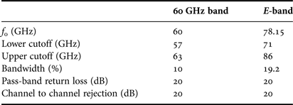
For demonstration, a three-pole bandpass filter was selected. The designs used 250 µm thick quartz substrate with relative permittivity ε r = 3.78 and gold metal layer; the CPW with dimensions 30 µm/300 µm/30 µm (G/S/G) was chosen. Two three-pole inductively coupled CPW filters were designed. The filter specifications are listed in Table 2. The out-of-band rejection was defined so that the 60 GHz band filter had rejection better than 20 dB in the E-band, with a symmetric arrangement for the E-band filter.
Table 2. Bandpass filter design specifications.
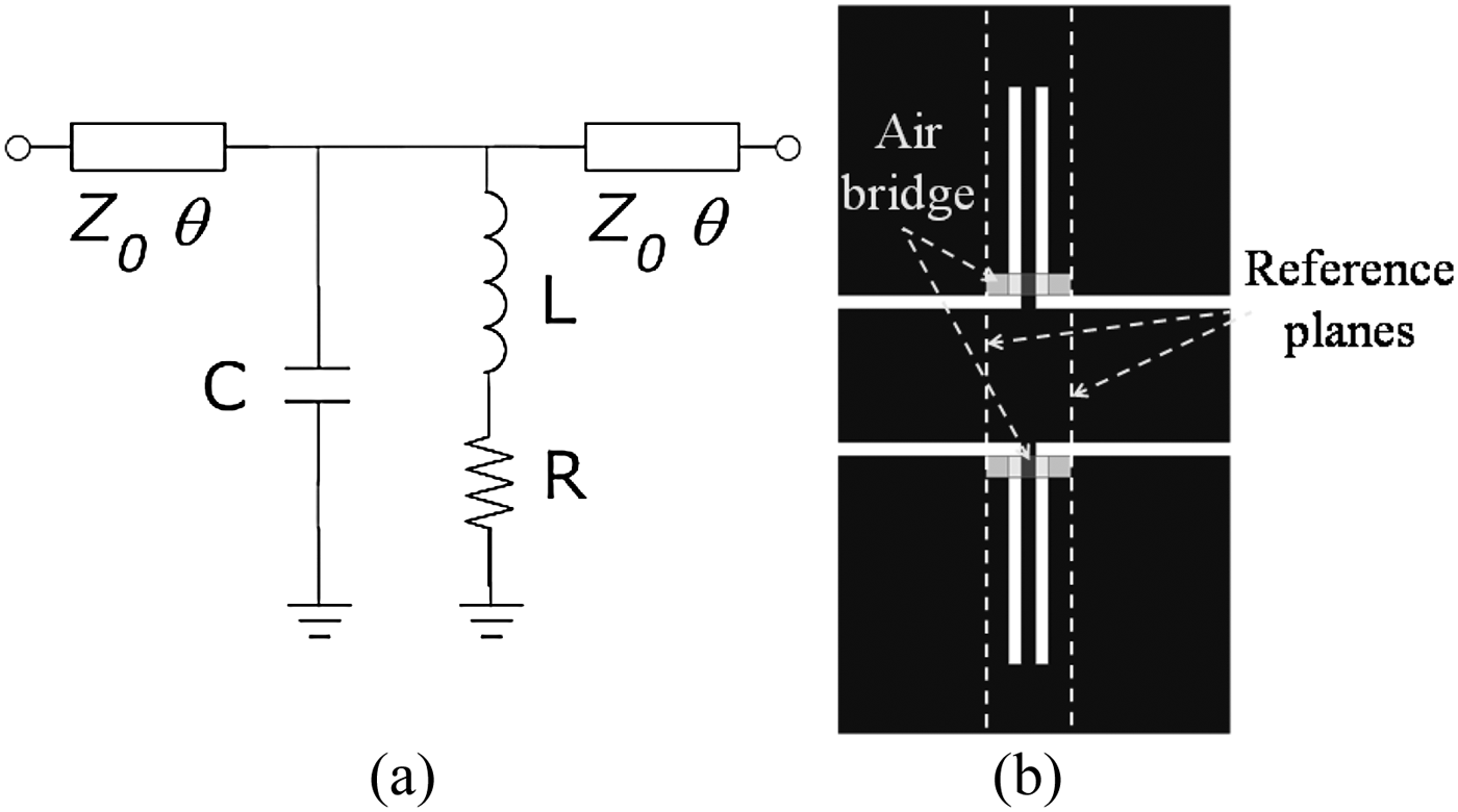
Shunt inductors are used as inverters for the filter. A shunt inductor has dimensions 30 µm/30 µm/30 µm (G/S/G) with 50 µm × 60 µm air-bridges. To increase the efficiency, the inverter circuit modeled after the electromagnetic (EM) was employed. The circuit model, shown in Fig. 1(a), is a modification of the model introduced in [Reference Chan, Daneshmand, Mansour and Ramer28]. The additional capacitance C leads to a much wider frequency bandwidth, while the resistance R corresponds to the loss. An optimization procedure can be used to acquire the circuit parameters such as Z 0, θ, C, and R. These values can be used to establish the relationship between inductance L and the shorted stub length, needed for simulation. In general, a 20 GHz bandwidth can be accurately modeled. The layout of the inductively coupled inverter is given in Fig. 1(b).
Fig. 1. Inductively coupled inverter: (a) circuit model; (b) layout.
To improve skirt rejection, a cascaded bandstop filter design was used. This had the advantage of maintaining the physical size of the overall filter while the pole number remaining unchanged. The bandstop filter could be modeled as a short-circuited stub, similar to the inductive inverter. However, as the stubs are much longer than the inductive inverters, air-bridges of size 20 µm × 360 µm, had to be placed between the two CPW grounds, in order to eliminate higher order modes. Lastly, to achieve a wide band, the circuit model, shown in Fig. 2(a), had to be altered and the inductor was replaced with a transmission line. The layout of the short-circuited stub is given in Fig. 2(b). The final circuit model of the inductively coupled filter, with cascaded bandstop filter and its layout, is illustrated in Figs 3(a) and 3(b). Circuit simulations of these two filters were performed with Agilent ADS. The parameters used in the simulations are listed in Table 3. These ADS circuit parameters were then translated into the physical layout dimensions, listed in Table 4, using space mapping techniques. EM simulations were performed using ANSYS HFSS. The filters with the cascaded bandstop filters were matched against the equivalent filters without the cascade in the corresponding frequency bands. The results appear in Fig. 3(c), where traces labeled S11SS and S21SS are the simulation results with the cascaded bandstop filter. It is seen that the filter skirt performance is improved. However, this comes with an increase in insertion loss, as an extra 1.5–2.0 dB loss is introduced. In simulations, these filters achieve Q-factor of 40 and the loss in the pass band is better than 4.4 dB, both for 60 GHz and E-band filters. Note that if the pole number were to increase to four, the insertion loss could only be better than 5 dB with the Q-factor of 40 and the skirt performance could not be matched to the proposed designs.
Fig. 2. Bandstop stub: (a) circuit model; (b) layout.
Fig. 3. Inductively coupled filter with cascaded bandstop filter: (a) topology; (b) layout; (c) simulated RF performance in the 60 GHz and E-band.
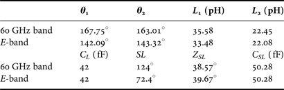
Table 3. Inductively coupled inverter bandpass filter parameters.
θ 1, θ 2 are the lengths of the resonators in degrees; L 1, L 2 are the inductances of the inverters; C L, C SL are the bridge capacitances of the inverter and bandstop filter; and Z SL is the length of the shunt short in degrees.
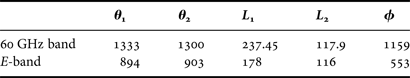
Table 4. Inductively coupled inverter bandpass filter physical dimensions.

All the dimensions are in μm. θ 1 and θ 2 are the physical lengths of the resonators; L 1 and L 2 are the lengths of the inductive inverters; and ϕ is the length of the shunt short circuit.
III. RECONFIGURABLE BANDPASS FILTER DESIGN
In order to achieve a fully reconfigurable bandpass operation that can switch between the 60 GHz and the E-bands within a single filter structure, the basic building blocks of a bandpass filter have to be altered. Three criteria need be fulfilled and, as we have two bandpass filters with different center frequencies, bandwidths and skirt performance, each of them must be addressed individually.
To address the difference in the center frequency, the half-wavelength resonators must be able to switch between the two bands. Here, an MEMS switched capacitor is used. When the MEMS switched capacitor is in its up-state, the resonator has to resonate at 78.15 GHz, while when it is in the down-state, it has to resonate at 60 GHz. We found that, in order to shift the resonance from 78.15 to 60 GHz, an up/down capacitance for the MEMS switched capacitor has to be 3.35. For a typical MEMS process, this ratio is controlled by the switched capacitor dimensions and the material used, and it is not very accommodating. Therefore, the fixed metal-air-metals (MAMs) have to be added in series with the MEMS switched capacitor to adjust the overall up/down capacitance ratio. Here the dimensions of the MEMS bridge are 20 µm in width and 360 µm in length with a simulated actuation voltage of 6 V. Both the switched capacitor and the MAM capacitors have an air gap of 2.5 µm. The MEMS switched capacitor also has an additional silicon nitride layer (0.3 µm) in the gap, to avoid the direct contact between the two metals, and a dielectric constant ε r = 7. Figure 4 shows the circuit model and the layout of this structure.
Fig. 4. Resonator with MEMS switched capacitor and MAM capacitors: (a) circuit model; (b) layout.
To deal with the difference in the percentage bandwidths, hence different coupling coefficients or inductance values, a novel inductive inverter is proposed and shown in Fig. 5. As can be seen in Fig. 5(a), a C MAM is connected in series with the inductor L. The added capacitor has the effect of altering the overall impedance of the inverter with respect to frequency. Instead of admittance 1/jωL + jwC b, the overall admittance is now jωC MAM/(1 − ω Reference Rebeiz2LC MAM) + jwC b, where C b is the unwanted parasitic from the air-bridge. With the correct selection of C MAM and L, it is possible to obtain the required coupling coefficients for both 60 GHz and E-band filters with fixed C MAM and L values. Therefore, no reconfigurable elements are needed for the inverters. It should be noted that this design method has a limitation; in order to have the correct combination of C MAM and L values for the different bands, the overall impedance of the inverter must increase with frequency. On the other hand, from a filter design perspective, the percentage bandwidth increases with the frequency; this is the case in our designs.
Fig. 5. Inductively coupled inverter: (a) circuit model; (b) layout.
To achieve a better roll-off at the rejection bands in both 60 GHz and E-band filters using a single layout, the bandstop stubs also require modification. In our design, MEMS switched capacitors are used in these stubs to provide different shunt-shorted lines for different frequency bands. Figure 6 shows the circuit model and the layout of this reconfigurable bandstop stub. As the circuit model illustrates, the shunt-shorted length is adjusted using the MEMS switched capacitor C MEMS to switch between ϕ 1 and ϕ 1 + ϕ 2 for E-band and 60 GHz band, respectively. These MEMS switched capacitors are of cantilever beam type, 20 µm wide and 220 µm long with 6 V actuation voltage.
Fig. 6. MEMS shunt shorted stubs: (a) circuit model; (b) layout.
Figure 7 shows the topology, layout and simulated RF performance, while Table 5 shows the list of dimensions of the RF MEMS reconfigurable inductively coupled bandpass filter. Simulation results showed that the insertion loss of better than 6.5 dB, and return loss of better than 15 dB can be achieved, both using this single reconfigurable structure. The isolation between these two modes is still better than 20 dB, similar to the case of each individual filter with the inserted bandstop filters. This MEMS reconfigurable filter corresponds to a three-pole filter with Q-factor around 20, but without the cascaded bandstop filters. In theory, this MEMS reconfigurable filter has a Q-factor around 35 when allowing for an extra 1.5–2.0 dB loss introduced by the cascaded bandstop filter to improve the skirt performance.
Fig. 7. RF MEMS reconfigurable inductively coupled filter with cascaded bandstop filters: (a) topology; (b) layout; (c) simulated RF performance in the 60 GHz and E-band.
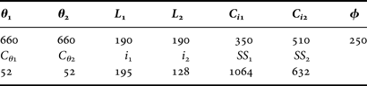
Table 5. Inductively coupled inverter bandpass filter physical dimensions.

All the dimensions are in μm. θ 1 and θ 2 are the physical lengths of the resonators in; L 1 and L 2 are the lengths of the inverters; C i1 and C i2 are the lengths of the MAM capacitors in the inverters; C θ1 and C θ2 are the lengths of the MAM capacitors in the resonators; i 1 and i 2 are the lengths of the inductive inverters; SS 1 and SS 2 are the lengths of the shunt short circuit.
IV. SWITCHABLE BANDPASS FILTERS
In order to analyze the performance of the fully integrated reconfigurable bandpass filter, a switchable bandpass filter is designed. To design a reconfigurable bandpass filter that is capable of switching between two ordinary filters at different bands, a RF MEMS single-pole double-throw (SPDT) switch is designed for up to 100 GHz. Figures 8(a) and 8(b) show the RF MEMS SPDT design and its simulated RF performance. A CPW G/S/G dimension of 10 µm/70 µm/10 µm and a back-to-back cantilever switches are used in this SPDT design. The MEMS cantilever switch has the beam length 160 µm and the width 70 µm. Isolation between all ports is better than 20 dB, up to 100 GHz. Simulations show better than 20 dB return loss and 1.5 dB insertion loss, both for 60 GHz and E-band; the simulated actuation voltage is 18 V.
Fig. 8. RF MEMS SPDT: (a) 3D model; (b) RF performance.
Figures 9(a) and 9(b) illustrate the layout of the RF MEMS switchable bandpass filter and the RF performance. The switchable bandpass filter is simulated when the 60 GHz and the E-band are individually activated. The RF MEMS SPDT offers a superior RF performance, and the switchable bandpass filter, both in 60 GHz and E-band operations, achieves a similar RF performance.
Fig. 9. RF MEMS switchable bandpass filter: (a) layout; (b) simulated RF performance showing the individual operation in the 60 GHz and E-band.
V. THE FABRICATED DEVICES AND MEASUREMENTS
The proposed structures are fabricated using a multi-layer gold deposition process. Figures 10(a) and 10(b) show the photographs of the fabricated 60 GHz and E-band switchable and compact reconfigurable bandpass filters. The size of the switchable filter is 8.35 mm × 5.45 mm while the compact reconfigurable filter is only 4.75 × 3.75 mm, which is about one quarter of the area size of the former. Figure 11 illustrates the measured RF performance for both filters, each operating separately at both bands; then compares them to their corresponding simulation results.
Fig. 10. Pictures of the fabricated filters: (a) reconfigurable; (b) switchable bandpass filters.
Fig. 11. Measurement results: (a) reconfigurable bandpass filter; (b) switchable bandpass filter.
A) Reconfigurable bandpass filter
The reconfigurable bandpass filter is successfully reconfigured, and designed to work in 60 GHz band and E-band using the embedded RF MEMS switched capacitors, without any reconfigurable filter inverters. The resonator switched capacitors were actuated to switch from E-band to 60 GHz, while the cantilever switched capacitors were actuated when the filter is in E-band mode. Actuation voltage of 10 V was used for all the switched capacitors in this design. It is seen that in the E-band mode (with the resonator-switched capacitors in the up-state, and the bandstop-switched capacitors actuated), insertion loss matches the simulation very well, except around the lower band edge. The measured insertion loss is better than 6.7 dB. The increase in the return loss around the lower frequency band edge could be due to the bandstop stubs switched capacitors performance. The down-state capacitance could be different compared with the simulation. This is due to the dielectric constant and layer thickness fabrication variations and tolerance of the silicon nitride. The measured return loss is better than 8 dB; this compared with over 17 dB in the simulation. This could be the result of the different capacitance in the inverter capacitances in the simulation. It can be seen in Fig. 11(b) that the inverter capacitors show different light reflections under the camera, which suggests that the upper metal layer of the capacitors is not completely flat.
A much higher discrepancy can be noticed between the simulation and the measured RF performance in the 60 GHz band mode. A center frequency shift and increase in the bandwidth can be noticed. The upper band edge had shifted by 2 GHz, from 63 to 65 GHz. This could be a combination of the explained inverter capacitance as well as the silicon nitride layer thickness and dielectric constant variations during the all three resonator-switched capacitors actuation. The performance of this filter is summarized in Table 6.
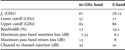
Table 6. Fabricated reconfigurable bandpass filter performance.
B) Switchable bandpass filter
The switchable filter measurements show very good correlation with the simulations, as illustrated in Fig. 11(b). The filter was switched to different bands using the RF MEMS SPDT switch and the actuation voltage was 25 V. The measured performance when switched to 60 GHz band, shows 1 GHz shift to lower frequency compared to simulation. The measured insertion loss of this filter is better than 7.2 dB when compared with 5 dB in the simulation. The E-band rejection is better than 30 dB. It could mainly be due to the fabrication tolerance, as the 60 GHz band filter is much narrower in the bandwidth. However, at 60 GHz band mode, the out-of-band S11 shows a dip at 85 GHz, to 10 dB, which was not noticed in the simulation. This suggested that the circuit is radiating at this frequency range.
The measured E-band filter performance also matches the simulation very well except at around the upper band edge. Their measured performance shows insertion loss better than 5.8 dB and return loss better than 15 dB. Again, the discrepancy could be mainly due to the fabrication tolerances. The performance of this filter is summarized in Table 7.
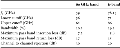
Table 7. Fabricated switchable bandpass filter performance.
VI. CONCLUSION
To the best of the authors’ knowledge, this is the first ever attempt to design and fabricate a filter tunable in 60 GHz and E-band. A novel mechanism is introduced in detail to reconfigure bandpass filter with different percentage bandwidth without tuning the inverters. Two reconfigurable bandpass filters, one fully integrated version targeting compactness, and one switchable version making use of RF MEMS SPDTs with back-to-back cantilevers, were designed, simulated, fabricated and tested. Both filters show good channel-to-channel isolation and are capable of operating between 60 GHz and E-band spectrums. They are demonstrated using RF MEMS switches and switched capacitors. New circuit models and designs were proposed for the inductively coupled inverters and for the short circuit bandstop filters, to achieve their reconfigurability. Measurement results show close agreement with the simulations.
King Yuk (Eric) Chan received his B.Sc. (with first class honors) and M. Eng. Sc. degrees in Electrical Engineering from the University of New South Wales (UNSW), Sydney, Australia in 2005 and 2006. He then continued his Ph.D. degree in Electrical Engineering under a joint project between the University of New South Wales (UNSW) and the Centre for Integrated RF Engineering (CIRFE), University of Waterloo, Canada. From 2007 to 2008, he was a research assistant at CIRFE, the University of Waterloo. He received a Postdoctoral Fellowship from UNSW and CSIRO ICT Centre in 2010 and 2011. He is currently a Research Associate at UNSW. His expertise includes, design skills on RF, microwave and millimeter-wave circuits, microfabrication process and development for RF and MEMS devices, and RF and MEMS devices data acquisition test bench skills.
Rodica Ramer (SM’06) received her Ph.D. degree in Solid State Physics from the University of Bucharest. Prior to this she was a senior Research Scientist in the Microwave laboratory in the National Centre for Nuclear Energy of Romania. From 1989 to 1992 she was a Visiting Professor and Research Associate in the Superconductivity laboratory at the University of Alabama, Microwave Laboratory at Colorado State University and in the School of EE at the University of Oklahoma. From 1993 she has been continuously with the School of Electrical Engineering and Telecommunications, at the University of New South Wales in Sydney Australia, where she is currently a Professor. During this time she spent extended sabbatical periods as Visiting Professor at the Microwave laboratory at Chiba University and at the National Taiwan University Electromagnetics laboratory. Her current research activities include the development of RF MEMS, new tunable structures, and radiowave propagation for wireless devices.