


I. INTRODUCTION
Space-division-multiplexing (SDM) wireless communication technology is attractive when constructing ubiquitous mobile networks supporting many wireless terminals and equipment with broadband wireless services by use of only a limited frequency band. Especially in millimeter-wave (MMW) frequency ranges, SDM technology is very effective owing to the straight propagation characteristics of MMW signals in a free space. Combination with the multiple-input and multiple-output (MIMO) technology is also attractive to secure numerous broadband wireless services. However, MMW signals are affected by relatively large propagation loss in air compared with microwave (MW) frequency ranges.
Radio-over-fiber technology is attractive for MMW wireless systems to transfer and relay MMW signals by use of silica optical fibers, which have the lowest propagation loss of 0.2 dB/km in any data transmission cable and have huge transmission bandwidth over THz [Reference Seeds and Williams1–Reference Iezekiel3]. Utilizing advanced photonic devices, such as wide-band optical amplifiers, high-precision optical frequency/phase shifters, high-speed vector modulators, high-extinction-ratio optical switches, and sharp-cut/narrow-band optical filters, the control of MMW signals in photonic domains is also possible with high accuracy. Therefore, the combination of MMW wireless technology with photonic technology is a promising way to construct ubiquitous broadband mobile communication networks in the future [Reference Seeds and Williams1–Reference Iezekiel3].
In order to construct MMW mobile communication systems combined with photonic technology, a device to convert MMW wireless signals to optical signals is very important. An interesting scheme is the integration of MMW planar antennas and high-speed electro-optic (EO) modulators on the same substrate [Reference Bridges, Sheehy and Schaffner4–Reference Wijayanto, Murata and Okamura7]. These are called “optical modulators using antenna-coupled electrodes”. Optical modulators using antenna-coupled electrodes for MMW frequency signals have many advantages; MMW signals received by planar antennas can be transferred to the electrodes for optical modulation with small loss and negligible crosstalk since the antennas and modulators are integrated on the same substrate and can be connected to each other with a short connection line. In addition, MMW signals received by an antenna array can be synthesized through successive EO modulation of lighwaves during their propagation under the antenna-coupled electrodes. Therefore, MMW signal synthesis circuits with precise tunings of amplitudes and phases for an array antenna are not necessary. Unwanted decay, coupling, and distortion of MMW signals, which might be caused by attenuations, transmissions, and reflections in MMW synthesis circuits with complicated delay lines, are eliminated and high-quality MMW signal synthesis can be obtained by photonic technologies.
Recently, we have proposed and developed a new antenna-coupled-electrode EO modulator utilizing a polarization-reversed structure of ferroelectric crystal substrates [Reference Murata, Suda and Okamura8]. This device can receive MMW signals and convert them to lightwave signals with low loss, low-crosstalk, and high-quality synthesis. In addition to these advantages of the optical modulator using antenna-coupled electrodes, this device can also discriminate between several wireless SDM signals, which are irradiated to the device, into different optical signals according to their irradiation angles at the same time owing to the selective conversion characteristics in polarization-reversed EO modulators. The basic operations of the proto-type device in MW frequency ranges have been reported in the experiments [Reference Murata, Suda and Okamura8–Reference Murata, Suda, Miyanaka and Okamura10]. However, the operational frequency of these devices remained low in MW frequency ranges; 15 GHz for [Reference Murata, Suda and Okamura8] and 25 GHz for [Reference Murata, Suda and Okamura9, Reference Murata, Suda, Miyanaka and Okamura10], although the SDM technique is more attractive in MMW frequency ranges.
In this paper, a new device operated in MMW frequency ranges around 40 GHz is reported on for the first time as far as we know. Conversion from wireless 40 GHz signals to optical signals was confirmed successfully. Wireless SDM signal discrimination with spatial channel isolation over 13 dB was also demonstrated using a fabricated device of only 30 mm long.
In the following sections, the structure of the proposed device, its operation principle, analysis, design, fabrication, and experimental demonstration are presented.
II. DEVICE STRUCTURE
Figure 1 shows the basic structure of the EO modulator, with the antenna-coupled electrodes and polarization-reversed structures, we have proposed. It consists of several (2–4) straight single-mode optical waveguides and an array of antenna-coupled modulation electrodes fabricated on a ferroelectric optical crystal substrate such as LiNbO3 or LiTaO3. EO polymers with controlled poling distributions of polarized molecules are also applicable for the substrate material. Several types of planar antennas, such as a patch antenna, a dipole/monopole antenna, a bow-tie antenna, and a slot antenna, are applicable for receiving wireless signals. Polarization-reversed structures are also fabricated into the ferroelectric optical crystal substrate along the optical waveguides to compensate for the degradation of the modulation effect by the transit time effect [Reference Yariv11] and to realize wireless signal discrimination according to their irradiation angles to the device [Reference Murata, Suda and Okamura8]. The number of straight optical waveguides corresponds to the number of SDM signal channels to enable discrimination.

Fig. 1. Basic structure of the proposed device.
Wireless MMW signals are received by the array of planar antennas and the received MMW signals are transferred to each of the connected modulation electrodes. Then, lightwaves propagating in the optical waveguides are modulated by the MMW signals successively in each modulation electrode. Therefore, the synthesis of the MMW signals received by the array of antennas and the signal conversion from MMW to lightwave are obtained. In this synthesis process, the polarization reversal structures enable us to make selective conversion of a MMW signal to a lightwave signal according to the irradiation angle along the optical waveguide. Therefore, the discrimination of wireless SDM signals is obtainable by adopting different polarization reversal patterns for the optical waveguides.
In this work, patch antennas, which are composed of a square micro-strip structure, were adopted as planar antennas, and resonant standing-wave modulation electrodes, which are composed of a coupled-micro-strip line (CMSL) with shorted ends, were adopted for the modulation electrodes as shown in Fig. 1. Each square patch antenna was connected to the resonant standing-wave electrode by use of a micro-strip feed line with an intrinsic impedance of 50 Ω.
III. OPERATION PRINCIPLE
The operation principle of the proposed device can be understood by considering the change in the modulation polarity caused by the polarization reversal in the ferroelectric crystal substrate. The top of the drawing in Fig. 2 shows the cross-sectional view of the device along the optical waveguide when a wireless MMW signal is irradiated to the device at an angle of θ. The wireless MMW signal is received by an array of equidistant antennas and the received MMW signal is transferred to a modulation electrode. Then, a standing-wave electric field is induced in each modulation electrode.

Fig. 2. Cross-sectional view of the proposed device along the optical waveguide, modulation electric fields on modulation electrode observed from a static system, modulation electric fields as would be observed at the propagating lightwave, and induced refractive index changes through the Pockels effect.
The standing-wave electric field in the modulation electrode can be expressed by the following equation:
where E 0 is the amplitude of the electric field, f m(x, z) is the distribution function of the MMW electric field in the x–z plane, n m is the effective refractive index of the MMW in the modulation electrode, k m is the wave number of the MMW in vacuum, and ω m is the angular frequency of the MMW signal.
Therefore, the modulation electric field Ehm at the hth standing-wave electrode can be expressed by the following equation when the supplied signals to modulation electrodes are at the same amplitude and are in the same phase:
where S is the separation between the antenna-coupled electrodes.
When the wireless MMW signal is irradiated to the device with an array of antenna-coupled electrodes at an angle of θ, the temporal phases of the MMW signals supplied to the modulation electrodes are changed according their separation S and the irradiation angle θ. By taking into account the temporal phase changes, the modulation field Ehm can be expressed by the following equation:
where n 0 is the refractive index of the MMW in air (=1). Equation (3) indicates that the temporal phase of the electric fields in the successive standing-wave electrodes changes according to the irradiation angle, θ, along the optical waveguide and the electrode separation, S, as shown in Fig. 2.
However, it takes finite time for the lightwave to pass through the waveguide, so the modulation electric field that would be observed by the wavefront of the lightwave propagating in the optical waveguide is not the same as the field observed by a person in the static system. The field, as would be observed at the lightwave, can be expressed by the following equation, taking into account the transit time of lightwave [Reference Yariv11]:
where n g is the group index of the lightwave, and ϕ (=− n gk my′) corresponds to the phase of the MMW signal when the lightwave was launched at the device. In equation (4), the sine function represents the spatial distribution of the standing wave along the resonant electrode. The cosine function represents the temporal and spatial phase change of the MMW signal as the lightwave propagates in the waveguide.
Typical examples of the electric fields expressed by equations (3) and (4) are also plotted in Fig. 2 when n g ~ n m/2. (This condition corresponds to the case of using a standard single-mode optical waveguide and thin metal-film-based coplanar/micro-strip line electrodes on a LiNbO3/LiTaO3 substrate [Reference Murata, Morimoto, Kobayashi and Yamamoto12].) In Fig. 2, the electric field as would be observed at the propagating lightwave contains positive and negative regions. The induced index change through the Pockels effect is proportional to the electric field. The total modulation index (depth) is obtained by the integral of the induced index change over all the modulation electrodes using the electric field that would be observed by the wavefront of the propagating lightwave instead of the electric field that would be observed in a static system. Therefore, it is rather degraded. So, the polarization reversal structures are introduced. By reversing the direction of spontaneous polarization at the regions with the reversed arrows in Fig. 2, the signs of the refractive index change become positive in all regions and a large modulation index is obtained. The modulation index (depth), D, in the polarization-reversed device can be expressed by the following equation:
where λ is the wavelength of the lightwave in vacuum, n e is the refractive index of the substrate material, r 33 is the Pockels coefficient for the substrate material, Γ is the overlapping factor between the lightwave guided mode distribution and the modulation electric field distribution (f m(x, z)), L e is the resonant electrode length, and N is the total number of the antenna-coupled electrodes. P(y) expresses the pattern of spontaneous polarization along the optical waveguide. P(y) is defined as +1 at a non-reversed region and −1 at a polarization-reversed region. The modulation index, D, is also a function of the angle of incidence, θ, since the phase of the electric field in each modulation electrode depends on the angle, θ. As a result, the directivity in the conversion from MMW signals to lightwave signals can be calculated using equation (5).
Typical examples of the calculated directivity in the conversion from MMW signals to lightwave signals are shown in Fig. 3(a). The corresponding polarization patterns are also shown in Fig. 3(b). By merely changing the polarization reversal patterns, the discrimination of wireless SDM signals are obtainable as shown in Fig. 3.

Fig. 3. Designed directivities in MMW-lightwave conversion (a) and corresponding polarization patterns (b) when S = 3.76 mm, L e = 1.7 mm, f m = 38 GHz, n m = 4.64, and n g = 2.2.
IV. ANALYSIS AND DESIGN
The antenna-coupled modulation electrode is a key component in the proposed device. Especially, precise tuning resonant frequencies and matching impedance values of the antenna and electrode are necessary for effective operation. Therefore, it was analyzed in detail by use of three-dimentional field analysis software, Ansoft HFSS.
First, the operational frequency was set at 38 GHz and the substrate material was assumed as 0.25-mm-thick z-cut LiTaO3. The length of the square patch antenna was also set at half a wavelength, and the length of the CMSL standing-wave electrode was set at one wavelength with short connections as shown in Fig. 4(b) (the second-order resonance condition). Both the antenna-coupled and ground electrodes were assumed to be composed of a 1-μm-thick Al film. A 0.2-μm-thick SiO2 buffer layer was also assumed to be set between the antenna-coupled electrode and the LiTaO3 substrate.

Fig. 4. Calculated surface electric field distribution on the antenna-coupled electrode under the normal irradiation of the linearly polarized MMW signal at the designed frequency of 38 GHz (a). The direction of the MMW signal polarization is indicated by the arrow. The designed pattern and parameters of the antenna-coupled electrodes (b).
Next, the patch antenna and the CMSL modulation electrodes were uncoupled and dummy input ports were attached to them with 50 Ω micro-strip feed lines. After that, they were analyzed independently in detail and their conditions for the resonance at 38 GHz and impedance matching at 50 Ω were derived.
Finally, a tuned patch antenna and CMSL were connected to each other by use of a 50 Ω micro-strip line, and the resonance characteristics were checked again under the irradiation of the plane wave MMW signals from the free space above the antenna. Figure 4(a) shows the calculated surface electric field under the normal irradiation of a linearly polarized 38 GHz MMW signal. It is shown that a strong standing-wave electric field is induced in the CMSL at 38 GHz. The designed parameters of the antenna-coupled electrodes are also shown in Fig. 4(b).
V. DEVICE FABRICATION
Based on the design, an SDM 38 GHz signal discrimination device was fabricated using z-cut congruent LiTaO3 crystal as a substrate material.
First, the polarization reversal patterns were fabricated onto a z-cut LiTaO3 crystal substrate of 0.25 mm thick and 30 mm long. The polarization reversal patterns of (B) and (C) in Fig. 3 were adopted for the fabrication. Therefore, discrimination between SDM wireless signals at an irradiation angle difference of 15° is expected by use of the device. For the fabrication of the polarization reversal structures, the pulse-voltage applying method [Reference Yamada, Nada, Saitoh and Watanabe13] was adopted. The pulse-voltage signal with a large amplitude and low repetition frequency (~1 kHz) was applied to the substrate. The required voltage was 5.5 kV to reverse the spontaneous polarization in the 0.25-mm-thick LiTaO3 crystal, which coincided well with the calculated value from the standard coercive force in LiTaO3 of 22 kV/mm [Reference Liu, Kitamura and Terabe14].
Next, straight single-mode optical channel waveguides were fabricated on the polarization-reversed substrate by use of the annealed proton-exchange method with melted benzoic acid at 240°C [Reference Tada, Murai, Nakabayashi, Iwashima and Ishikawa15, Reference Murata and Okamura16]. The core width and depth of the fabricated waveguides were 3.0 µm and 1.5 µm, respectively. The guided-mode characteristics in the fabricated waveguides were verified by use of the prism coupling method in the preliminary experiments [Reference Murata and Okamura16]. The waveguide separation was 30 µm, which was enough to isolate the two-channel optical waveguides.
Finally, an eight-element array of 1-μm-thick Al antenna-coupled electrodes was formed onto the optical waveguides after a deposition of a 0.2-μm-thick SiO2 buffer layer for optical waveguides. The SiO2 film was formed by use of magnetron RF sputtering and the Al film was formed by use of electron-beam vapour deposition. For the patterning of the antenna-coupled electrodes, a standard photolithography technique was used. The reverse side of the substrate was also covered by a 1-μm-thick layer of Al film for the ground electrode. The photograph of the fabricated device just before the final deposition of the reverse side for the ground electrode is shown in Fig. 5.

Fig. 5. Photograph of the fabricated device.
VI. EXPERIMENTS
The performance of the fabricated device was measured using the experimental set-up shown in Fig. 6. The CW lightwave with a narrow spectrum from a distributed-feedback laser of 1.55 µm was divided and launched to the optical waveguides of the fabricated device by use of single-mode optical fibers. At the same time, a MMW signal from an oscillator was amplified and irradiated to the device by use of a standard horn antenna (Flann Microwave Ltd. Model 22240-20, Gain ~20 dB at 38 GHz, Aperture size 35 × 25 mm2). The optical spectrum of the output lightwaves was monitored by use of an optical spectrum analyzer. We then changed the MMW signal polarization, frequency, power, irradiation angle θ, and distance between the horn antenna and the device.

Fig. 6. Experimental set-up.
Figure 7 shows typical examples of the measured optical spectrum when the MMW frequency and power were 38 GHz and 18 dBm with θ = 0° (normal to the device). Optical modulation sidebands were observed clearly when the polarization of the MMW signal was along the X-direction shown in the inset of Fig. 7. On the contrary, no optical sideband was observed when the MMW polarization was along the Y-direction as shown in Fig. 7. This clear polarization dependence completely matched that of the designed antenna-coupled electrode, where the antenna and the modulation electrode are connected with the micro-strip line parallel to the X-direction.
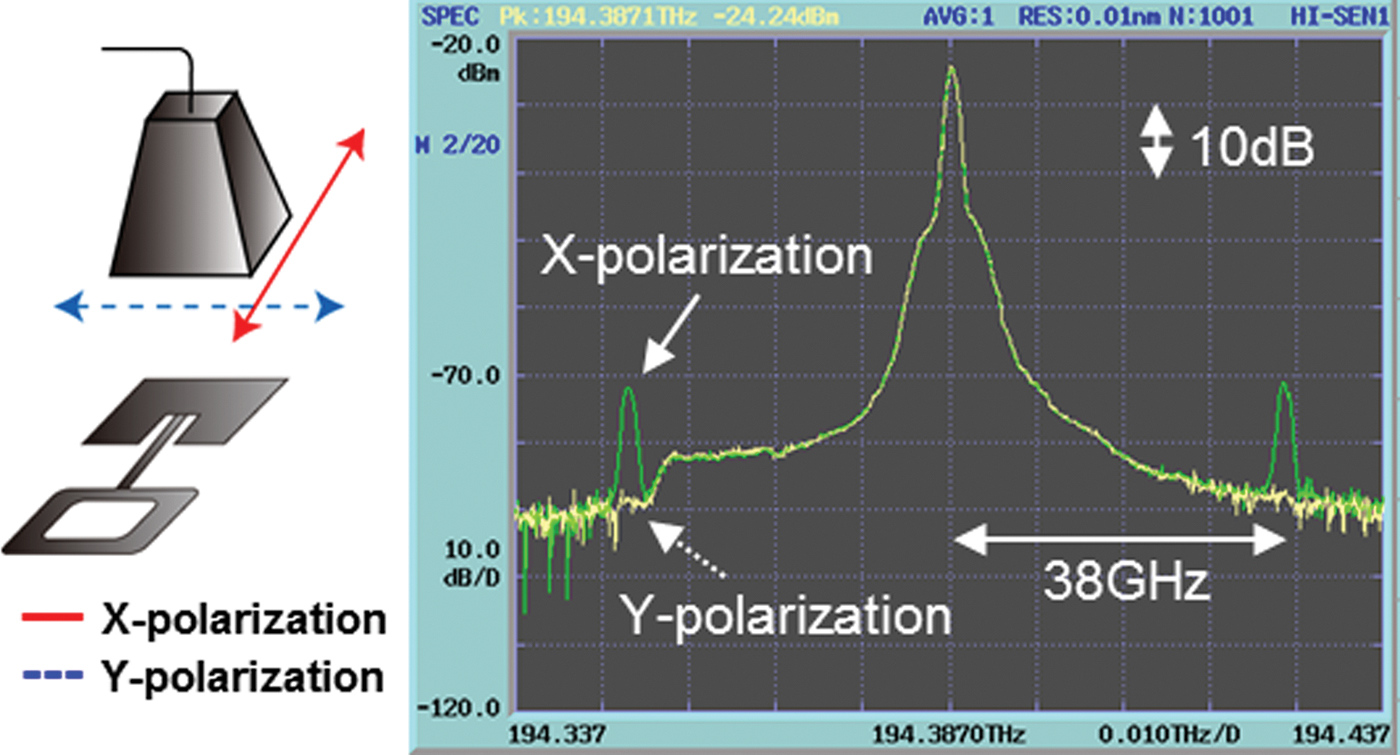
Fig. 7. Measured optical spectra for X- and Y-polarized MMW irradiation.
Figure 8 shows the measured dependence of the modulation efficiency by the distance between the device and the emitting horn antenna. The fabricated device was an optical phase modulator. Therefore, a modulation index can be adopted as a measure for modulation efficiency, and a modulation index is calculated from the spectrum ratio between the optical carrier and the first sideband as long as the modulation index value is rather smaller than unity. Optical modulation sidebands were observed under the irradiation of a 38 GHz signal of 18 dBm with a separation up to 1 m between the emission horn antenna and the device. Figure 9 shows the measured frequency dependence of optical modulation efficiency (the ratio between the optical carrier and first sideband intensities). The peak modulation frequency was in good agreement with the designed operational frequency of the antenna-coupled electrode.

Fig. 8. Measured dependence of the fabricated device to the distance between the emission horn antenna and the device.

Fig. 9. Measured frequency dependence of the fabricated device.
Figure 10 shows the change of the optical modulation spectra at 38 GHz by the polarization reversal patterns. For the 38 GHz signal irradiation normal to the device (θ = 0°), clear optical modulation sidebands were observed from the optical waveguide with the polarization reversal pattern of (C) defined in Fig. 4, and negligible sidebands were observed from the optical waveguide with the pattern of (B) as shown in Fig. 10(a). On the contrary, when the irradiation angle was θ = 15°, clear optical sidebands were observed from the optical waveguide with the pattern (B), but almost no sidebands were observed from the optical waveguide with the pattern (C) as shown in Fig. 10(b). Figure 11 shows the measured directivity in the conversion from the 38 GHz MMW signals to optical signals for the polarization reversal patterns of (B) and (C). These are in good agreement with the theoretically calculated ones. The measured spatial channel isolation was over 13 dB with a device of 30 mm long. Therefore, the basic operation of the proposed device was confirmed successfully.

Fig. 10. Measured optical spectra from the two optical waveguides with different polarization reversal patterns of (B) and (C) shown in Fig. 4. The irradiation angle to the device was θ = 0° (a), and θ = +15° (b).

Fig. 11. Measured directivities in MMW-lightwave conversion for patterns (B) and (C).
The measured modulation efficiency (modulation index) was rather small compared to standard optical phase modulators for optical communication systems and MW photonics systems. However, by utilizing advanced photonic devices, such as sharp-cut optical filers and optical amplifiers, effective optical modulation efficiency can be rather enhanced (>20 dB), which was also verified in the experiments using the fabricated device and clear demodulated 38 GHz signals were obtained with a carrier to noise (C/N) ratio over 25 dB. The details of the enhancement of the effective modulation efficiency and reconversion to MMW signals will be reported elsewhere.
By increasing the number of antenna-coupled electrodes and tuning the polarization reversal patterns, the SDM channel isolation can be enhanced further and the irradiation angle difference to be discriminated can be narrow. For example, using an array of antenna-coupled electrodes with 12 elements at 38 GHz, the SDM signal discrimination with an irradiation angle difference of 10° is obtainable. The number of SDM channels to be discriminated corresponds to the number of optical waveguides under the modulation electrodes. Four optical waveguides can be adopted in the proposed device as shown in Fig. 1, and four SDM channels can be discriminated between at the same time. By using other modulation electrode structures based on coplanar MW/MMW waveguides and double-electrode structures, 6–12 SDM channels can be discriminated between.
VII. CONCLUSIONS
We proposed a new EO device for both converting wireless MMW signals to optical signals and discriminating between SDM signals according to their irradiation angle along an optical waveguide. The synthesis conditions of wireless signals through EO modulation can be tuned almost arbitrarily by use of the polarization reversal structure of the ferroelectric optical crystals. The discrimination of the 38 GHz wireless SDM signals using the proposed antenna-coupled-electrode EO modulator was demonstrated successfully. By utilizing advanced photonic devices for fiber communication systems such as sharp-cut optical filers and optical amplifiers, effective optical modulation efficiency can be greatly enhanced (>20 dB), which was also verified in the experiments using the fabricated device. Two-dimentional SDM signals may also be discriminated between multiple combinations of the proposed devices and with external optical interferometer circuits.
Now, further improvement of the conversion efficiency is underway by using different substrate materials; a low-dielectric constant material is used for the antennas and a ferroelectric crystal is used for the optical modulation. The application to SDM MIMO systems is another topic for future research.
ACKNOWLEDGEMENTS
The authors thank Drs. Tetsuya Kawanishi and Hidehisa Shiomi for their helpful advice on the analysis and experiments. This work was supported in part by the Grants-in-Aid for Scientific Research from the Ministry of Education, Science, Sports and Culture, Japan.
 Hiroshi Murata received the B.Eng., M.Eng., and D.Eng. degrees in electrical engineering from Osaka University, Osaka, Japan in 1988, 1990, and 1998, respectively, for studies on the guided-wave systems with third-order optical nonlinearity and their applications to all-optical functional devices. In 1991, he joined the Department of Electrical Engineering, Faculty of Engineering Science, Osaka University, where he is now Associate Professor in the Division of Advanced Electronics and Optical Science. His work is concerned with integrated optics, nonlinear optics, and microwave photonics. He is the author or co-author of more than 100 technical publications in these areas and also holds several patents. Prof. Murata is an Associate Editor of the IEICE Electronics Express (ELEX) in the IEICE, Japan and was the Guest Editor of the Journal Advances in OptoElectronics in the Special Issue: “Progress in Domain-Engineered Photonic Materials”, in 2007–2008. He is also a member of the EuMA, the IEEE Photonics and MTT societies, the OSA, the JSAP, the IEICE, and the Laser Society of Japan. Prof. Murata was the recipient of the 35th European Microwave Conference Microwave Prize in 2005.
 Ryota Miyanaka received the B.Eng. and M.Eng. degrees in electrical engineering from Osaka University, Osaka, Japan in 2009 and 2011, respectively, for studies on the electro-optic modulator using antenna-couple electrodes and polarization reversal structures. In 2011, he joined Panasonic Corporation. His works are concerned with the development of electric appliances and related technologies.
 Yasuyuki Okamura received the B.Eng., M.Eng., and D.Eng. degrees in electrical engineering from Osaka University, Osaka, Japan in 1973, 1975, and 1978, respectively, for studies on the anisotropic optical waveguides. From 1978 to 1981 he worked for Kokusai Denshin Denwa Corporation (KDD), where he was engaged in developing ultra-low loss optical fibers. From July 1981 to March 1996, he was with the Department of Electrical Engineering, Faculty of Engineering Science, Osaka University. From April 1996 to March 2003, he was a Professor of the Department of Optomechatronics, Faculty of Systems Engineering, Wakayama University, Wakayama, Japan. From April 2003, he has been a Professor of the Division of Advanced Electronics and Optical Science, Graduate School of Engineering Science, Osaka University. He is now Dean of the Graduate School of Engineering Science at Osaka University. His current work has been concerned with optical engineering, electro-magnetic theory, microwave circuits and antennas, and random media. Prof. Okamura is a member of the Institute of Electrical and Electronics Engineers, the Japan Society of Applied Physics, and the Institute of Electronics, Information and Communication Engineers.


