


I. INTRODUCTION
The need to increase the performance and speed in complementary metal-oxide semiconductor (CMOS) technology has required new strategies extending beyond the traditional scaling of device dimensions. For example, the application of strain within the current-carrying regions of CMOS devices can be tailored to improve the carrier mobility. The link between the resistivity and the applied stress in semiconductors, described by Bardeen and Shockley (Reference Bardeen and Shockley1950) and quantified by Smith (Reference Smith1954), also relates the carrier mobility to the local state of strain. In order to exploit this effect to enhance the carrier mobility, CMOS devices can be manufactured using strained layers adjacent to the current-conducting paths in the Si. Existing methods employed to induce strain in the channel regions involve either the deposition of heteroepitaxial SiGe or SiC into Si trenches or the deposition of stressed films above the transistors. In the first case, regions containing SiGe, which possess a larger lattice parameter than that of Si, induce a compressive strain in the plane of the Si channel (Rim et al., Reference Rim, Hoyt and Gibbons2000), whereas SiC regions, with a smaller equilibrium lattice parameter, create a tensile in-plane strain. A corresponding increase in hole mobility, required for PFET devices, can be produced through the use of compressively stressed Si (Thompson et al., Reference Thompson, Armstrong, Auth, Cea, Chau, Glass, Hoffman, Klaus, Ma, McIntyre, Murthy, Obradovic, Shifren, Sivakumar, Tyagi, Ghani, Mistry, Bohr and El-Mansy2004). For the case of stressed overlayer films, such as silicon nitride (Ito et al., Reference Ito, Namba, Hirata, Ando, Koyama, Ikezawa, Suzuki, Saitoh and Horiuchi2002), the edges of the gate and spacer regions above the Si channel create stress concentrations, resulting in strain distributions in the channel region of the SOI that possess the same sign of in-plane strain as in the stressed film.
The experimental determination of strain fields within individual CMOS structures requires significant effort. While micro-Raman spectroscopy is capable of measuring deformation at a submicron resolution (DeWolf et al., Reference DeWolf, Norstrom and Maes1993), the technique relies on an a priori assumption of the dimensionality of the strain tensor within the measurement volume. It also requires a calibration to correlate peak shifts to stress values in contrast to X-ray diffraction which directly determines the Si lattice spacing. The laser-induced heating of the sample can also lead to errors in peak shift measurements particularly in the case of individual structures in silicon-on-insulator (SOI) layers (Georgi et al., Reference Georgi, Hecker and Zschech2007). Although transmission electron microscopy (TEM) based techniques, such as convergent beam electron diffraction (CBED), possess an extremely small spot size (on the order of several nanometers), the significant sample preparation required to produce an electron-transparent specimen modifies the stress state of the original features. CBED also represents a correlative technique, where simulations of high order Laue zone (HOLZ) line shifts are required to deduce the lattice deformation (Hue et al., Reference Hue, Hytch, Bender, Houdeliier and Claverie2008), a procedure that becomes difficult for SOI-based structures due to HOLZ line splitting. Among the techniques that allow for in situ detection at a submicron scale, synchrotron-based X-ray microbeam measurements (Murray et al., Reference Murray, Yan, Noyan, Cai and Lai2005; Murray et al., Reference Murray, Saenger, Kalenci, Polvino, Noyan, Lai and Cai2008; Murray et al., Reference Murray, Ren, Ying, Polvino and Noyan2009), which determine components of the local elastic

Figure 1. Cross-sectional TEM image of (a) e-SiC/SOI channel device and (b) sample geometry near an edge in the overlying Si3N4 feature.
strain tensor along particular directions, are better suited.
Traditional device modeling often applies the simplification of uniform stress distributions within the CMOS devices. Because the actual channel regions possess heterogeneous strain distributions in both of these implementations, a more comprehensive modeling of the band structure realignment is required to determine the overall device response. In addition, the modeling of the piezoresistive behavior in Si-based systems, which strongly depends on the substrate doping and carrier density in the inversion channel (Colman et al., Reference Colman, Bate and Mize1968), would benefit from a more accurate description of the strain fields. The measurement of the distribution of strain across the current-carrying paths of the device and the surrounding environment is critical to predicting device performance. This paper describes our work on the experimental mapping and mechanical modeling of strain distributions induced in semiconductor features based on the two approaches.
II. EXPERIMENTAL
Devices possessing embedded stressor materials were fabricated from boron doped 55-nm thick SOI layers on 300-mm diameter Si (001) substrates. The source and drain regions were recessed by approximately 40 nm from the SOI surface followed by epitaxial growth of Si1−xCx with a C content, x, of 1.1%. The remaining SOI thickness under the e-SiC features, approximately 15 nm thick, was kept as a template onto which the strained e-SiC could be deposited. Because C has a smaller lattice parameter than that of Si, the e-SiC structures possess in-plane tensile stress, which is transferred into the adjacent SOI. The devices under investigation consisted of 60 nm long SOI channels with adjacent e-SiC source and drain regions approximately 1.85 μm in length. The width of the device, corresponding to the distance between the horizontal gate contacts, was approximately 17.5 μm. Gates consisting of polycrystalline silicon and silicon oxide spacers were also fabricated above the SOI channel. The cross-sectional TEM image in Figure 1a depicts the SOI channel region surrounded by the e-SiC features, which are approximately 40 nm in thickness and the underlying buried oxide (BOX) layer that isolates the SOI from the Si substrate. To obtain a reference value for the unrelaxed SiC strain, square pads 200 μm in length, consisting of silicon-carbon that was heteroepitaxially deposited on SOI, were also characterized. Measurements of the Si (008) (2θ∼109.19°) and e-SiC (008) (2θ∼110.56°) diffraction peaks were obtained during the same θ/2θ scan in regions when the incident X-ray beam intercepted both types of features.
To investigate the stress fields due to overlying stressor features, compressively stressed Si3N4 films of approximately 105-nm thickness were deposited onto 200-mm diameter SOI substrates. Features were lithographically defined in a photoresist layer and then transferred to the Si3N4 layer by reactive ion etching resulting in a matrix of rectilinear features possessing lengths of 2048 μm and widths ranging from 1 to 2048 μm. The cross-sectional geometry of the features includes a 140-nm thick BOX composed of SiO2 between the SOI and the underlying Si substrate, as seen in Figure 1b. X-ray microdiffraction measurements were conducted at several locations across the Si3N4 features to determine the strain distributions within the SOI layer. Four sites were chosen consisting of Si3N4 features possessing widths of approximately 1.0, 1.5, 2.5, and 2048 μm. In all cases, a plane strain assumption could be made due to the geometry of the Si3N4 features, whose lengths were over 2 mm. Strain mapping within the SOI layer was performed by acquiring θ/2θ scans and translating the sample in 0.2-μm increments.
The diffraction facilities at the 2ID-D beamline at Argonne National Laboratory’s Advanced Photon Source were used for the X-ray microdiffraction measurements. A description of the experimental setup can be found in Murray et al. (Reference Murray, Yan, Noyan, Cai and Lai2005). Fresnel zone plate focusing optics produced a beam footprint on the sample of approximately 0.25 by 0.3 μm. Diffraction optics consisted of vertical receiving slits of approximately 300-μm spacing, corresponding to an acceptance angle of 0.026° for the embedded features and 100-μm spacing for the overlying stressor structures, placed directly in front of a scintillation detector. A beam energy of 11.2 keV (λ=1.1070 Å) was chosen so that the angle of the Si (008) diffraction peak could be measured at a relatively large value (2θ∼109°). Because the crystallographic orientations of the substrate and SOI layers were offset by at least 0.24°, diffraction information from the sample could be separately resolved between both of these regions.
III. MODELING
It is necessary to establish a correlation between the X-ray diffraction measurements and mechanical models to properly interpret these measurements and to assess the validity of the models. Three models, all based on linear elasticity, were used in the analyses.
A. Eshelby inclusion
For the e-SiC features, mechanical modeling was performed using an analytical method based on Eshelby inclusions in a semi-infinite elastic medium (Mindlin and Cheng, Reference Mindlin and Cheng1950). It is based on a model refined by Davies (Reference Davies2003) for rectangular inclusions under a plane strain condition. The displacement, w, in the out-of-plane direction is used to calculate the depth-averaged out-of-plane strain, ε¯33, in all regions of interest:
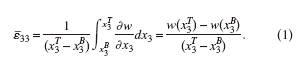
For the SOI channel, the top and bottom surfaces lie at x3=0 and 55 nm, respectively. The SOI underneath the e-SiC regions resides between x3=40 and 55 nm, with the e-SiC occupying the region between x3=0 and 40 nm. The model assumes that the entire half-space possesses the same elastic properties and that the top surface is free. Since the underlying BOX does not significantly impact the overlying mechanical behavior of the SOI and e-SiC structures, the first assumption is valid. However, the presence of polysilicon gates and spacers will modify the actual strain distributions within the features.
B. Anisotropic edge force
We first approximated the stress distribution due to overlying Si3N4 features by using an analytical model based on an edge force applied at the SOI surface at the position of the Si3N4 feature edge. The formulation is based on the model developed by Michell (Michell, Reference Michell1900) but extended to an elastically anisotropic half-space Si substrate (Murray, Reference Murray2006). In this application, both the BOX layer and the constraint provided by the overlying Si3N4 are ignored. Because the silicon nitride feature edges were patterned along the 〈110〉 directions in the samples under investigation, the edge force is applied parallel to [110]. The depth-averaged out-of-plane strain is calculated by integrating the normal stresses over the diffracting volume, which is completely defined by the SOI layer possessing a thickness t. As calculated in Murray (Reference Murray2006), the stress components for the 〈110〉 (001) Si orientation possess the following form:
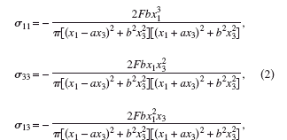
where a=0.4472, b=0.9393, and F refers to the magnitude of the edge force:
where σ B represents the residual biaxial stress in the blanket film, and h is the film thickness.
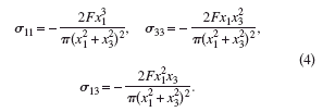
For the elastically isotropic case, corresponding to a=0 and b=1, the stress components in Eq. 2. take the familiar form:
C. Numerical model
A two-dimensional computational model using the boundary element method (BEM) was also implemented (Murray et al., Reference Murray, Saenger, Kalenci, Polvino, Noyan, Lai and Cai2008) based on the formulation of Rizzo (Reference Rizzo1967). Several advantages exist for BEM over variational formulations such as those used in FEM: (1) the solution is not approximated by using interpolation functions within the discretized domain; (2) singularities in the solution are often better captured due to the integral nature of BEM; and (3) only the surfaces of the bodies need to be discretized rather than the entire body resulting in fewer elements and correspondingly fewer equations to solve.
Although elastic isotropy was assumed in both the overlying film features and the underlying substrate, the BEM model allows for a more accurate representation of the feature geometry. Again, the presence of a BOX layer was not incorporated into the mechanical modeling. We assume perfect bonding at the interfaces so that the displacements are equivalent in both bodies and the sum of the tractions is zero at the interface. The integration of the influence coefficients was performed analytically where constant-value surface elements were used in the calculation.
The displacement field, u i, is calculated due to the influence of the eigenstrain, Δ ε, in the Si3N4 features as well as the original traction boundary conditions. Because the displacement fields for the effective and actual cases are identical: u ieff=u i. However, the solution of the stress components, σ i j, within the body must be transformed back from the effective traction boundary conditions:
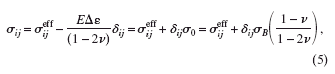
where σ 0 represents the eigenstress in the material and σ B is the residual blanket film stress. Equation 5. shows that the eigenstress and eigenstrain are equivalent representations of the same effect, where the eigenstrain Δ ε=−σ 0(1−2ν)/E for a dilatational eigenstress, σ 0, or Δ ε=−σ B(1−ν)/E for a blanket film stress, σ B.
The out-of-plane displacement at the free surface or along the Si/Si3N4 interface, w(x 3=0), was calculated using the nodal value of the displacement at the element centers. The vertical displacement was subsequently calculated for the interior points corresponding to x 3=−tSOI. The Poisson’s ratios of the Si and Si3N4 were assumed to be 0.28 and 0.3, respectively, and the Young’s moduli were both assumed to be 160 GPa.
IV. RESULTS AND DISCUSSION
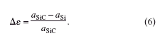
The equilibrium lattice spacings for both Si, a Si, and Si1−xCx, aSiC must be determined to convert the measured Si (008) and e-SiC (008) diffraction peaks into strain. The underlying Si substrate provides a reference value for aSi. However, aSiC will depend on the substitutional C concentration within the film. The lattice mismatch between a heteroepitaxially strained Si1−xCx layer and the underlying Si can be represented by an eigenstrain, Δ ε:
A linear elastic, fully strained e-SiC feature deposited on a Si (001) template, which possesses cubic elastic symmetry, will exhibit an isotropic, in-plane biaxial stress (σ 11=σ 22). If a plane stress assumption is also used for the out-of-plane stress (σ 33=0), then the relationship between the out-of-plane strain, ε 33, and Δ ε is (Murray et al., Reference Murray, Yan, Noyan, Cai and Lai2005)
where S i j k l C refer to the single-crystal compliance tensor components of Si1−xCx. Because of the low C concentration present in the e-SiC, the compliance components can be approximated by those of Si. From Brantley (Reference Brantley1973), these single-crystal compliance values are S1111C=7.68×10⁻³GPa−1 and S1122C=−2.14×10⁻³ GPa−1. Equations 6 d7. can be combined to form the following:
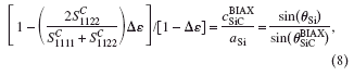
where c SiCBIAX is the Si1–xCx out-of-plane lattice spacing and Bragg’s law was used to relate the measured diffraction peaks to lattice spacings. The Gaussian fits of the Si substrate (008) and e-SiC (008) peak centers from the 200-μm pad regions yielded an eigenstrain, Δ ε, of −0.472(2)% or an effective out-of-plane strain, ε 33BIAX, of −0.365% in the e-SiC, corresponding to approximately 1% volume fraction of C substituted into the Si lattice. A negative eigenstrain indicates that the e-SiC in-plane stress is tensile.
For the general case of a strained e-SiC feature, the depth-averaged out-of-plane lattice spacing, c¯SiC, measured in the feature and the out-of-plane strain, ε¯33, are directly related through linear elasticity: c¯SiC=a SiC(1+ε¯33). With knowledge of Δ ε, the corresponding equation between the measured out-of-plane lattice spacing can be determined:
For the SOI region, the depth-averaged lattice spacings, c¯Si, can directly be transformed into out-of-plane strain values:
Figure 2 shows the diffracted intensities as a function of 2θ with the X-ray beam centered on the SOI channel region and positioned 0.8 μm away from the channel. The measured out-of-plane strains in the e-SiC, as calculated using Eq. 9., are approximately −0.355±0.003% within the vicinity of the channel and −0.350±0.003% 0.8 μm away from the channel. The broad Si (008) peak in the measurement conducted 0.8 μm from the channel represents the thin SOI layer underneath the e-SiC features and corresponds to a small, tensile out-of-plane strain of 74×10−6 from Eq. 10.. This positive value of out-of-plane strain reflects the compensating in-plane compression generated underneath the e-SiC stressor structure. The difference between the two SOI diffraction peaks measured away from and at the channel contains the depth-averaged strain information from the SOI

Figure 2. (Color online) Comparison of the (008) diffraction measurements conducted in the SOI channel region (circles) and 0.8 μm away from the channel (squares).
channel corresponding to an out-of-plane compressive strain of −0.167±0.007%.
To compare the measurements to the simulated values generated using the Eshelby inclusion model, the depth-averaged out-of-plane strain was also laterally averaged within the entire channel region for the SOI strain and within a 0.25-μm region, corresponding to the X-ray beam width, in the e-SiC region approximately 0.8 μm away from the channel. The calculated out-of-plane strains in these regions are 0.752Δ ε for e-SiC and 0.391Δ ε for the SOI channel. Because Δ ε was determined to be −0.472% from the 200-μm wide e-SiC pads, the predicted out-of-plane strains for the e-SiC feature and SOI channel are −0.355% and −0.176%, respectively, as listed in Table I. The measured strains in the e-SiC regions (−0.35% and −0.355%) match the calculated values well, and the out-of-plane SOI channel strain represents approximately 95% of the predicted quantity. Therefore, the impact of the constraint imposed by the overlying gate and spacer regions, which is not treated by the Eshelby inclusion model, can be no more than 5% of the measured strain. In fact, this effect is probably less than 5%, since the SOI regions underneath the e-SiC features intercepted by the incident X-ray beam possess a compensating, tensile out-of-plane strain that reduces the magnitude of the measured strain.
A comparison of the edge-force and BEM calculations to the data for the out-of-plane SOI strain across the edge of the 2048×2048 μ m2 Si3N4 feature is depicted in Figure 3. Because this Si3N4 feature edge is separated from any other feature by at least 2 mm, it can be considered a single isolated edge. A fit to the X-ray diffraction information to the BEM model indicates that a compressive blanket film stress,
TABLE I. Comparison of depth-averaged out-of-plane strain, ε 33, in the e-SiC and SOI regions calculated using the Eshelby inclusion model and measured using XRD.
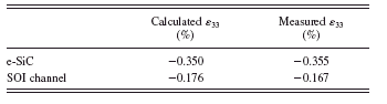

Figure 3. (Color online) Comparison of the experimentally measured and BEM calculated depth-averaged strain distribution, ε 33, across the edge of the 2048×2048 μ m2 Si3N4 feature.
σ B, of −2.5 GPa is present in the Si3N4, in agreement with values obtained independently from wafer curvature measurements on blanket films (−2.47±0.2 GPa). The BEM calculated values capture the asymmetry exhibited in the strain distribution across the Si3N4 feature edge location, although the calculated profile slightly underestimates the strain outside of the feature. In the case of the edge-force model, the strain distribution in the SOI layer that possesses a free surface is fairly well modeled but the predicted values diverge from the measured strain in the SOI underneath the Si3N4 feature within 1 μm from the feature edge or approximately ten times the Si3N4 feature thickness. This discrepancy can be attributed to the assumptions inherent to the edge-force model. Because the interaction between the film and substrate is assumed to occur at the feature edge only, every other section of the Si surface is considered traction-free resulting in a purely antisymmetric strain distribution in the underlying SOI layer. The actual constraint imposed by the presence of the Si3N4 feature decreases the out-of-plane strain underneath the Si3N4 as exhibited by the X-ray diffraction results. Peel and shear stresses exist at the Si3N4/SOI interface which cannot be captured by the edge-force model, which assumes that the top SOI surface is traction-free. However, the edge-force model reasonably predicts the strain distributions at sufficiently large distances from the edge (greater than ten times the Si3N4 feature thickness) where the stress distribution in the Si3N4 feature produced by the presence of a free edge does not impact the underlying SOI strain.
Both the experimental results and modeling clearly illustrate the generation of strain fields in the vicinity of a free edge in a material possessing an eigenstress. For all of the subsequent modeling results, a blanket film stress, σ B, of −2.5 GPa, as determined from the 2048×2048 μ m2 feature, will be used in the calculations for the smaller feature sizes. Because the geometry and the elastic constants of the Si3N4 structures and the SOI are known, the eigenstress represents the only free parameter for both the BEM and edge-force models.
Figure 4 shows the measured and calculated out-of-plane SOI strain distributions under the 1-μm, 1.5-μm, and 2.5-μm wide Si3N4 features, respectively. We observe that the BEM simulations reproduce the depth-averaged out-of-plane SOI strain very well for all of the measured feature widths. It must be noted that the strain gradients present under the feature edges are too large to be captured by the microbeam so that the measured strain at these points represents a convolution of the actual SOI strain distribution and the X-ray beam shape. However, there is a close correspondence between the BEM calculated values and the measured strain distribution at a distance of 0.2 μm from the feature edges. In contrast, the edge-force simulations do not match the measured strain values in the SOI about the narrow features. However, as the feature width increases, the out-of-plane strain values under the feature centers start to approach those predicted by the edge-force model particularly at the

Figure 4. (Color online) Comparison of the experimentally measured and calculated depth-averaged strain distribution, ε 33, across the 2048×1-μm, 2048×1.5-μm, and 2048×2.5-μm wide Si3N4 features.
center of the 2.5-μm wide feature. Based on the results in Figure 3 for a single edge, we would expect to observe discrepancies between the edge-force simulations and the measured strain in the SOI layer underneath the Si3N4 features possessing widths less than 2 μm due to the overlapping strain fields from both edges. In addition, the maxima in the depth-averaged strain observed in the SOI outside of the Si3N4 features increase as the feature width increases so that the maximum SOI strain outside of the 2.5-μm wide feature already approaches 84% of the maximum value observed outside of the 2048-μm wide feature. Although the edge-force simulations predict larger strain values than those observed in the SOI regions outside of the Si3N4 features, the discrepancy decreases with increasing feature width.
V. SUMMARY
Measurements of the depth-averaged SOI strain, as induced by overlying stressed Si3N4 thin film features and embedded SiC structures, were performed using microbeam X-ray diffraction. The out-of-plane strain measurements from the e-SiC regions, with a tensile eigenstrain of −0.472%, are in good agreement with the values predicted by an Eshelby inclusion model. The out-of-plane compressive strain of −0.167% detected in the SOI channel is approximately 95% of the calculated value. Both the surrounding SOI contained within the diffracting volume underneath the e-SiC features and the overlying constraint imposed by gate and spacer regions impact the measured SOI channel strain. The Eshelby model is capable of capturing the depth-averaged strain in the SOI channels to within 5% of the measured values. A comparison of the simulated strain distributions using BEM indicated that a compressive blanket film stress of −2.5 GPa is present in the Si3N4 features. Although an anisotropic, elastic edge-force model reproduced the observed SOI strain at distances greater than 1 μm, or ten times the Si3N4 film thickness, from the edge of wide features, the fit was poor in the case of narrow feature widths where the strain fields produced by the stress concentrations at the feature edges overlapped. The presence of peel and shear stresses along the Si3N4/SOI interface, ignored in the edge-force model but incorporated in the BEM simulations, is critical to the accurate modeling of the mechanical response of these thin film composite systems. In addition, the observed strain gradients induced in the SOI layer must be taken into account to properly calculate device carrier mobility.
ACKNOWLEDGMENTS
The authors would like to thank Dr. K. L. Saenger and Dr. Z. Ren of IBM Research for the sample manufacture. Work at the Advanced Photon Source was supported by the U.S. Department of Energy, Office of Science, Office of Basic Energy Sciences, under Contract No. DE-AC02-06CH11357.


