


I. Introduction
Amplifiers with broad bandwidth are needed for ultra-wideband systems, electronic warfare, high-speed optical communications, instrumentation, radar, and general purpose amplifiers [Reference Virdee and Virdee1]. These broadband amplifiers have routinely been designed using the traveling-wave-amplifier (TWA) configuration, since it is well established and is suitable for MMIC implementation. The TWA configuration incorporates the input and output capacitances of the device into the distributed structure [Reference Ayasli, Mozzi, Vorhaus, Reynolds and Pucel2, Reference Ayasli, Reynolds, Mozzi and Hanes3] and is relatively easy to design. In addition, the semiconductors employed have been GaAs [Reference Oda4], InP, and more recently SiGe [Reference Kudszus, Shahani, Pavan, Shaeffer and Tarsia5]. Wide bandgap GaN/SiC devices are projected to deliver higher power and broadband performance. Few TWAs have been demonstrated in GaN technology [Reference Meliani, Behtash, Würfl, Heinrich and Tränkle6].
In most broadband amplifier configurations, including that for the TWA, it is difficult to have a design with performance extended to very low frequencies. The other broadband configurations include cascode amplifiers [Reference Martin7], feedback amplifiers [Reference Darwish, Boutros, Luo, Huebschman, Viveiros and Hung8], and the classical reactively matched amplifiers [Reference Palmer, Saunier and Williams9]. The cascode configuration, using two-device cell per stage can offer the added gain to the overall amplifier. In the feedback configuration, an RC network between the drain and gate (or collector and base) provides negative feedback to achieve flat-gain response, and to provide stability. In reactively matched amplifiers, the input and output networks produce an appropriate mismatch to reduce the low-frequency gain. In addition to bandwidth, there are many other characteristics to consider when evaluating amplifier performance including stability, efficiency, output power, and complexity of bias and RF designs.
The present design uses devices (cells) that are connected DC/RF in series. The concept of series biased Field Effect Transistor (FET) was reported with GaAs devices [Reference Ezzeddine, Hung and Huang10], and later implemented in MMIC configuration [Reference Peterson11]. It provides high power-added efficiency through the use of the high voltage/low current on RF-paralleled FET cells, thus reducing the I2R losses in the DC distribution networks at the MMIC level, as well as at the system level when multiple power amplifiers are employed as in a phased-array system. A modified high-voltage/low-current novel broadband configuration, termed the HiFET, has achieved significant bandwidth and output power. It was originally implemented in GaAs FETs at microwave frequencies (both in discrete [Reference Ezzeddine and Huang12] and MMIC circuits [Reference Ezzeddine and Huang13]), and has recently been simulated using Si-Complementary Metal Oxide Semiconductor (CMOS) [Reference Wu, Tao, Basaran, Luger, Dettmann and Berroth14], implemented using InGaP HBTs [Reference Lei, Tsai, Lin and Wang15], and SiGe Hetero-junction Bipolar Transistor (HBT) with an integrated current mirrors for biasing [Reference Farmer, Darwish and Zaghloul16]. The concept is to stack FET transistors (or HBTs) serially such that their drain (or collector) supply voltages add up whereas their drain (or collector) currents remain constant.
The current paper presents the implementation of a configuration comprising series HEMTs (S-HEMTs) with the corresponding simulated and measured results. The S-HEMT configuration differs from the HiFET configuration in two important aspects. In the S-HEMT configuration, the matching conditions are optimized for broadband operation, instead of high-power operation. This brings the reactively matched circuit techniques [Reference Palmer, Saunier and Williams9] into the circuit design as will be explained in the following section. In addition, in the S-HEMT configuration, no feedback resistors are used; this leads to some important advantages as will also be explained in the following section.
The GaN technology has the potential for amplifiers with high-power densities, high efficiencies, and high-temperature operation, up to mm-wave frequencies [Reference Palacios17, Reference Darwish, Huebschman, Viveiros and Hung18]. For this reason, the present implementation of the S-HEMT configuration has been accomplished in the GaN/SiC technology. The S-HEMT configuration may be biased at high voltage, quadrupling the drain voltage in the present design. A GaN MMIC amplifier with a gain of 12 ± 2 dB, from 0.1 to 27 GHz, is presented. To our knowledge, this is among the broadest bandwidths achieved in the GaN technology.
II. GaN Mmic Design
The AlGaN/GaN HEMT epitaxial layers were on Metal-Organic Chemical Vapor Deposition (MOCVD) grown 3-in semi-insulating 6H-SiC substrates. The material has an AlN nucleation layer on SiC substrates. The epitaxial layers consist of an un-doped GaN channel layer, an AlN sub-Schottky-barrier layer, an un-doped AlGaN Schottky layer, and a GaN cap layer. Device isolations were formed by mesa etch using reactive-ion etching. Ti-/Al-based metal stack and rapid thermal anneal at 850°C were used for source and drain ohmic contacts. Contact resistances were measured to be less than 0.4 Ω mm. Gate openings were defined by e-beam lithography. Gates were recessed using Inductively Coupled Plasma (ICP) etch followed by Pt/Au metal deposition. Drain current density of about 1000 mA/mm was achieved at 10 V drain voltage and 1 V gate voltage. The MMIC design and fabrication were based on the device reported in [Reference Kao, Lee, Hajji, Saunier and Tserng19].
The GaN MMIC schematic is shown in Fig. 1. The circuit is composed of a stack of four HEMT devices. The four transistors, named HEMT1, HEMT2, HEMT3, and HEMT4, are in series (DC and RF). This circuit topology differs from the HiFET configuration in that the feedback resistors are absent, and the matching conditions are different. The feedback resistors in the original HiFET design provide (a) biasing for the gates of HEMT2, HEMT3, and HEMT4; (b) negative feedback at low frequencies; and (c) a reasonable match for HEMT1 and HEMT2. In the present circuit design, HEMT2's gate bias was controlled directly through the bias pad Vg2, and so on, see Fig. 1. This provided greater biasing flexibility and covers the first function of the feedback resistors. Second, when the frequency of operation becomes very high (beyond Ku-band), the resistors that used to provide negative feedback may cause positive feedback and introduce stability problems. This would be detrimental to broadband high-frequency operation. Third, having greater flexibility in the inter-stage matching allows the use of reactive matching techniques for gain shaping. In the present case, reactive matching was implemented to obtain a flat-gain response.

Fig. 1. GaN MMIC schematic.
For the input match design, it is implemented to provide reasonable input matching and stability across the designed bandwidth, and facilitate biasing through an integrated RF choke. The inter-stage matching, output matching, and gate capacitances (C1–C3) are optimized for flat broad bandwidth operation. The output match is intentionally mismatched at the low frequency to reduce the HEMT's natural high gain at low frequency. At the high frequency (K-band), the output match was designed to provide a reasonable (not optimum) match for power. In the circuit optimization, a goal with a greater weight was placed on obtaining a flat broadband gain than on achieving optimum power match.
All device cells (HEMT1, HEMT2, HEMT3, and HEMT4) have the same total gate width periphery, 6 (fingers) × 60 µm. The HEMT periphery was an optimization parameter. The design was fabricated using a 0.25 µm GaN on SiC process. The device has a cutoff frequency f t of 60 GHz, and a maximum oscillation frequency f max of 80 GHz. A photo of the S-HEMT GaN MMIC is shown in Fig. 2. The simulated performance is shown in Fig. 3.

Fig. 2. Photo of S-HEMT GaN MMIC. The chip area was 2.7 mm2 (0.95 × 2.875 mm2).
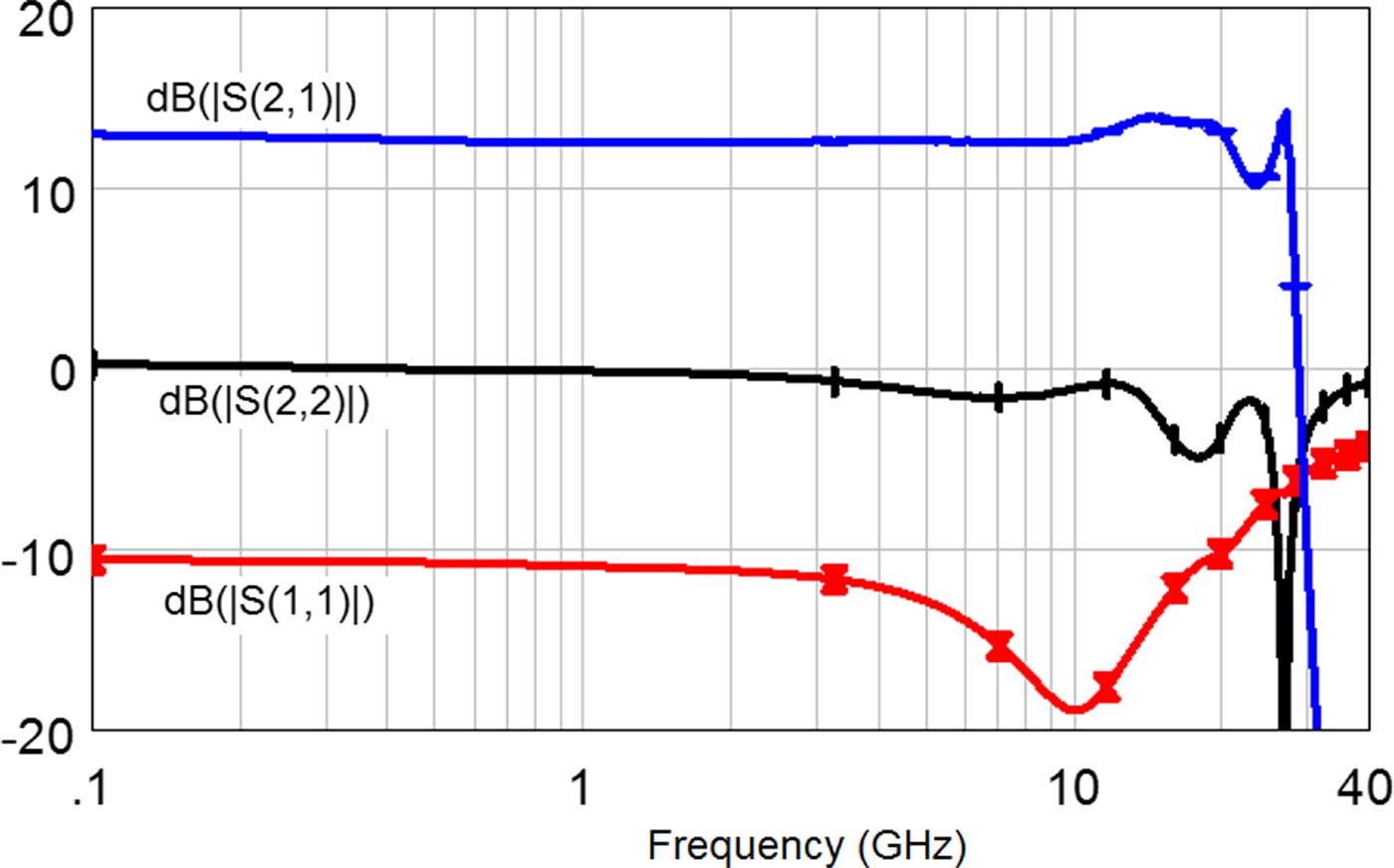
Fig. 3. Simulated performance of S-HEMT GaN MMIC.
The unconditional stability of the amplifier was checked by ensuring that the input and output stability parameter μ, is greater than 1 for all frequencies (Fig. 4). The stability of the individual HEMTs/stages was also verified through simulation. For the individual stages, conditional stability is sufficient given that the source and load of each stage (the preceding and following stage, respectively) is fixed, and not an arbitrary impedance. The values of the gate capacitors were appropriately selected. Similar selection procedure has also been successfully applied to the design in [Reference Farmer, Darwish and Zaghloul16].

Fig. 4. Stability parameter for overall MMIC PA and for the individual stages. The thick traces (circle and triangle symbol) are the stability parameters of the overall MMIC amplifier.
The overall gain flatness is the result of each HEMT contributing gain in part of the frequency band. Figure 5 shows the gain of stage 1 which is due to HEMT1, stage 2 (due to HEMT2), stage 3 (due to HEMT3), and stage 4 (due to HEMT4). The gain of stages 2, 3, and 4 were offset by 10, 20, and 30 dB, respectively, to make the figure clearer. The overall MMIC gain is the sum of the gains. As the figure indicates, HEMT1 contributes gain up to 18.7 GHz. Beyond that, the gain rolls off. On the other hand, HEMT2's gain contribution peaks at 25 GHz, and HEMT3's gain peaks at 27.5 GHz. This explains why the stack of four HEMTs gives broader bandwidth (0.1–27 GHz) than the stack of two HEMTs (0.1–20 GHz) reported in [Reference Darwish, Hung, Viveiros and Kao20]. The performance of the MMIC in [Reference Darwish, Hung, Viveiros and Kao20] is shown in Figs 6 and 7. Again, HEMT1 (stage 1) has a 3-dB roll off at 14 GHz, whereas HEMT2 peaks around 20 GHz. So the broadband flat gain is the result of the two stages covering different portions of the spectrum. In the current design (with four stages), the gain can be extended beyond that available from the stack of two due to the additional coverage from HEMT3 and HEMT4.

Fig. 5. Gain of each stage and of overall MMIC. For clarity, the gain of stage 2 is offset by 10 dB, of 3 by 20 dB, and of 4 by 30 dB. The overall gain is the sum of all the gains.

Fig. 6. Measured performance the stack of two GaN MMIC.

Fig. 7. Gain of each stage and of overall MMIC for stack of two GaN MMIC. For clarity, the gain of stage 2 is offset by 10 dB. The overall gain is the sum of the two gains.
In the broadband MMIC design, the modeling of the upper HEMTs (HEMT2, HEMT3, and HEMT4) required additional effort, because they are not in the common source configuration. In most general cases, the device that is available for measurement and modeling is a common source HEMT. However, the requirement here is to have a full three-port (drain, gate, and source) device model. In the present case, HEMT2, for example, is not a common gate device as C1 is a small capacitor and cannot be assumed to provide low impedance to ground. Thus, HEMT2 is almost a floating gate device. This poses two further considerations: device modeling and circuit stability. The modeling consideration was resolved by measuring and modeling a via-hole-grounded common source HEMT. Then, the via effects and source bus (transmission line) were de-embedded. After that, the new gate bus was modeled based on EM simulation, and a three-port model was produced. Figure 8 shows the EM structure used for modeling the input/output bus of HEMT2, HEMT3, and HEMT4. The stability consideration was resolved with the circuit designed to satisfy the stability condition for each HEMT stage, and for the amplifier as a whole to be unconditionally stable over all frequencies.

Fig. 8. EM structure for modeling the input bus (left) and output bus (right) of HEMT2, HEMT3, and HEMT4.
III. Measured Results
The measured MMIC performance is shown in Fig. 9. The measurement was performed both on wafer and in a fixture. Figure 9 is the measurement done on the fixture. The drain bias was varied from 40 to 120 V with little effect on the small-signal performance. The input match is better than 10 dB for most of the bands through the use of lossy input matching.

Fig. 9. Measured S-HEMT small-signal performance.
The output match is similar to the simulated value. The reason for the deficient output return loss over the low-frequency region is that it is intentionally mismatched to reduce the amplifier's gain in the low-frequency region. The output return loss will improve significantly once a few of the S-HEMT amplifier cells are combined in parallel to achieve higher power. Another approach to improve the output return loss is to add a shunt resistor to the output line, similar to the output terminating resistor in TWA amplifiers. There, the output terminating resistor provides improved output matching, at the expense of gain and power reduction. The circuit was stable at all biases and no instability issues were encountered.
The frequency response was measured down to 100 MHz. However, it is expected that the circuit's flat-gain performance extends to even lower frequencies. The output power was well matched across the Ku-band. The amplifier was measured at 17 GHz, 48 V, 125 mA, and exhibited 30 dBm (1 W) at 1-dB gain compression, see Fig. 10.

Fig. 10. Measured S-HEMT output power, gain, and PAE performance at 17 GHz.
IV. Conclusion
A multi-octave, wideband amplifier based on an S-HEMT configuration concept was presented. The amplifier was designed to achieve broadband performance with a flat-gain response. It achieved a gain response of 12 ± 2 dB, from 0.1 to 27 GHz, and operates with a wide range of drain bias voltages (40–120 V). The presented circuit demonstrated multi-octave-band performance without the use of the conventional TWA design approach. The unique S-HEMT circuit offers another approach to the design library available to the broadband MMIC designer. Its drain efficiency is similar to that of TWAs. The MMIC amplifier covers the operation frequencies from L- to K-band simultaneously, as well as lower frequencies (below 1 GHz). The circuit demonstrates GaN technology's potential for broadband applications. The present device (with f t of 60 GHz/f max of 80 GHz) was only used as a means for demonstrating the concept. However, much higher performance devices have recently been achieved and should enable improved bandwidth and output power performance.
ACKNOWLEDGEMENTS
The authors would like to thank Ming-Yih Kao and Cathy Lee of TriQuint Semicondcutor for their support in the fabrication of the MMICs.
 Ali M. Darwish received his B.Sc. and M.S. degrees with honors in electrical engineering from University of Maryland, College Park, in 1990 and 1992, respectively. He was awarded the National Science Foundation (NSF) fellowship. He received his Ph.D. degree from the Massachusetts Institute of Technology, Cambridge, MA, in 1996. In 1990 he joined COMSAT Labs where he conducted the experimental work for his M.S. thesis. In 1992 he served as a research assistant in the optics and quantum electronics group at MIT. In 1997, he co-founded Amcom Communications, Inc., a leading supplier of high-power microwave devices. In May 2003, he joined the Army Research Lab. (ARL), RF electronics division, Adelphi, Maryland. In 2007, he joined the American University in Cairo. Prof. Darwish is a senior member of the IEEE, was awarded the distinguished teaching award, outstanding service award at AUC, and the exceptional service award at ARL.
 H. Alfred Hung received the S.B., E.E. from the Massachusetts Institute of Technology, Cambridge, MA, and the M.S. and Ph.D. from Cornell University, Ithaca, NY. He is currently with the Army Research Laboratory, Adelphi, MD, and has initiated R&D programs on III–V, wideband gap, and Si-based electronics devices/circuits and heterogeneous integration technologies for sensors, imaging, communications, and multi-function, phased-array systems. He has also been the program manager for a number of advanced technology programs. Previously, he held research, functional, and program management positions at COMSAT Laboratories, Raytheon, TRW, and GTS, and worked on various technologies and subsystems for satellite, wireless, and military system applications. He was also an adjunct professor with the George Washington University. Dr. Hung has authored or co-authored over 130 publications, and has also been active in the technical committees of various symposia and served as a reviewer for IEEE Transactions and Proceedings, and other technical journals.
 Edward Viveiros received his BSEE in 1984 from Rutgers University and his MSEE in 1991 from The John Hopkins University. He is a team leader in the RF Electronics Branch at the U.S. Army Research Laboratory. He currently leads R&D efforts in advanced device, circuit, and integration technologies including GaAs, InP, GaN, SiGe, and MEMs for SATCOM, radar, and multi-function RF applications.
 Amr A. Ibrahim was born in Cairo in 1987. He received his B.Sc. (with honors) degree in electrical engineering from Ain Shams University, Cairo, Egypt, in 2009. He is currently working toward the M.Sc. degree at the same university. His master research involves the use of metamaterials in designing enhanced performance RF components and antennas. He was appointed as a T.A. by the Faculty of Engineering, Ain Shams University since his graduation. From August 2009 to August 2010, he served as a R.A. at the American University in Cairo. In summer of 2010, he had an internship at the chair of microwave and communication engineering at the Otto-Von-Guericke University, Magdeburg, Germany, where he developed a three-layer 8 × 8 butler matrix used in feeding antenna arrays utilized in MRI systems.


