I. INTRODUCTION
Since the release of Ultra-Wideband (UWB) frequency spectrum covering 3.1–10.6 GHz for commercial communication application in 2002, UWB filters with single or multi-notched bands having the capabilities to avoid the interference from Wireless Local Area Network systems (WLAN) have been rapidly developed. IEEE 802.11a operates around 5 GHz, which overlaps the band of UWB signals regulated by the Federal Communications Commission (FCC) and can bring significant interference to UWB systems [1]. For such circumstances a UWB filter is required to provide rejection capability in a band from 5 to 6 GHz [Reference Hong and Lancaster2, Reference Hsu, Yeh, Chen and Chuang3]. Different methods and structures based on Multiple Mode Resonators (MMRs) [Reference Zhu, Sun and Menzel4–Reference Xu, Miao and Wu9], Stub Loaded Resonator (SLR) [Reference Hong and Lancaster2, Reference Hsu, Yeh, Chen and Chuang3, Reference Xu, Wu, Kang and Miao10, Reference Wk and Chen11] and ring resonator [Reference Kim and Cheng12] have been used to develop UWB band pass filters whose compact size, low cost and insertion loss, good selectivity, and out of band rejection performance. Authors in [Reference Liu, Jiang and Li5] proposed a notched band UWB filter with adjustable notch band by employing a radial UIR/SIR loaded stub. However, the frequency response is not sharp enough in the lower or upper transition bands. A filter consisting of MMR with stepped impedance configuration and a parasitic coupled line, suffered from the same problem [Reference Pirani, Nourinia and Ghobadi6]. A cascade connection of defected microstrip structures (DMS) was used to realize a wide bandpass filter (BPF) in [Reference Fallahzadeh and Tayarani13]. In spite of presented relevant analysis, the structure failed to provide an acceptable insertion loss and roll off. In a similar method, stub loaded MMR was used in [Reference Chu, Wu and Tian14] to achieve an UWB filter. However; a notch band was not provided to eliminate the interference frequencies to FCC band.
In this paper a novel compact UWB BPF along with all theoretical aspects are presented. Firstly, interdigital coupled lines are designed to create strong coupling at f c = 6.39 GHz, which is needed for UWB application. Secondly, rectangular stubs and resonator M which is composed of three sub-resonators are adopted in the interdigital coupled lines to introduce notch band, required transmission zeroes and to decrease lower and upper transition bands. The roles of each section in filter's performance are theoretically discussed based on even and odd mode analysis. All structures are simulated and measured by using Rogers-RT-Duroid 5880(ε re = 2.2, h = 31 mil, tan δ = 0.0009).
II. DESIGN AND ANALYSIS OF THE NOVEL UWB RESONATOR
A) Realization of sharp roll-off and notch band
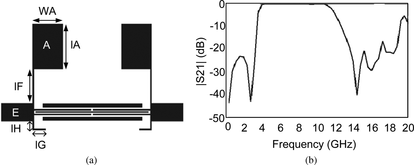
Interdigital coupling resonators are presented in Fig. 1(a). These resonators are used instead of direct coupling to provide strong coupling introducing capacitance effects which results in flat passband. As it is clear from Fig. 1(b), the lower and upper transition bands are not small enough. To solve the problem, transmission zeroes need to be added in the frequency response. So, two rectangular stubs are implemented in both the ports of resonator, as shown in Fig. 2(a). The rectangular resonators cause two transmission nulls at around 2 GHz which decreases the lower transition band greatly. To sharpen the upper roll-off, a novel resonator (M) is designed and added in the middle of interdigital resonator. This resonator not only suppresses WLAN frequencies, but also decreases the upper transition band simultaneously. Resonator M consists of three sections as depicted in Fig. 3. Radial Stub Loaded Resonator (RSLR) is employed in M to reduce the total circuit size as compared with the UWB BPF based on the conventional SLR. It can be seen from Fig. 4(b) that this resonator was designed to create two transmission nulls at around 5 and 12 GHz which the former introduces a practical notch band and the later provides a sharp roll-off in the upper passband edge.
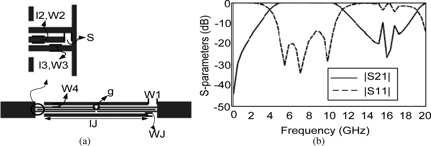
Fig. 1. Interdigital coupled resonator: (a) layout, W 1 = 1, l2 = 15, W 2 = 0.2, l3 = 7.5, W 3 = 0.2, W4 = 0.2,g = 0.24, S = 0.1, lJ = 13.23, and WJ = 0.50 (all in mm); (b) frequency response.

Fig. 2. Combination of two rectangular stubs: (a) layout, lA = 6, WA = 3.8, lF = 4.44, WF = 0.2, lG = 1.5, WG = 0.2, lH = 1.14, WH = 0.2, and WE = 2.42 (all in mm); (b) frequency response.

Fig. 3. (a) Resonator M, (b) RSLR, (c) Decagonal patch, lB = 3.4 mm,WB = 1.18 mm, θ = 82.3°, Ro = 3.865, Ri = 0.8, and lk = 3.65.

Fig. 4. Combination of resonator M and the interdigital coupled lines.
III. MODAL ANALYSIS
A) Resonance frequency realization
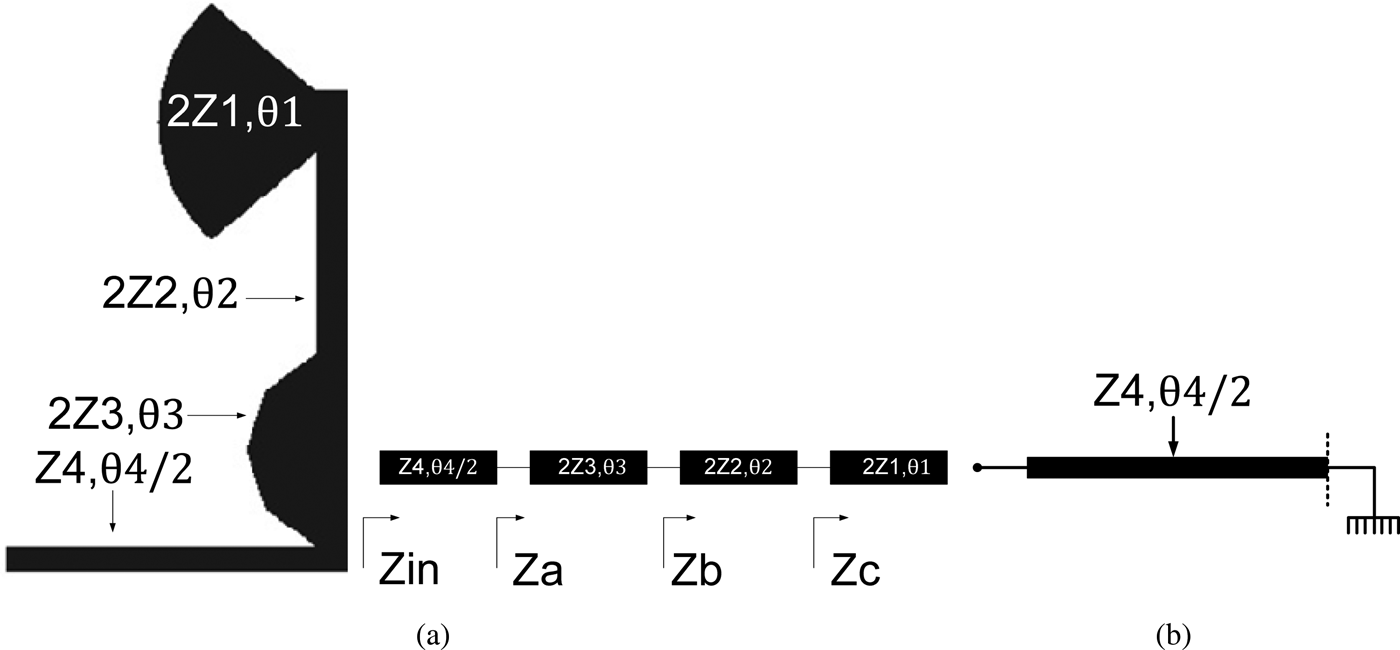
The equivalent transmission line model of the proposed UWB filter is depicted in Fig. 5. The MMR in Fig. 4 can be split into the equivalent circuits for the even and odd modes along the symmetric plane of the filter. For odd mode excitation, the central plane will be short-circuited whose equivalent circuit is shown in Fig. 5(b).

Fig. 5. Equivalent transmission line model of the proposed UWB filter. (a) Even mode, (b) odd mode.
The resulting input admittance for the odd-mode can be calculated as (1), where θ 4 = βL 4 is the electric length of the Microstrip line. From the resonance condition (when Y ino = 0), the fundamental odd-mode resonant frequency of the open-SLR is obtained 8.2 GHz by (2). In (2), c is the speed of light in free space and ε eff denotes the effective dielectric constant.
 $${Y_{ino}} = \displaystyle{{{Y_4}} \over {j\tan ({\theta _4}/2)}}, $$
 $${f_{0,odd}} = \displaystyle{{(2n - 1)c} \over {2{L_4}\sqrt {{\varepsilon _{eff}}}}}. $$
Similarly, for the even-mode excitation, the central plane is open-circuited whose equivalent circuit is shown in Fig. 5(a). For simplicity in calculation of even and mode resonance frequencies, the first two segments in Fig. 5(a) are firstly considered. So, Y ine is calculated for lines with Z 4 and 2Z 3 impedances (equations (3)). The same way can be generalized for the third and fourth sections and as a result the final equation for the even mode resonance frequencies is yielded in (7).
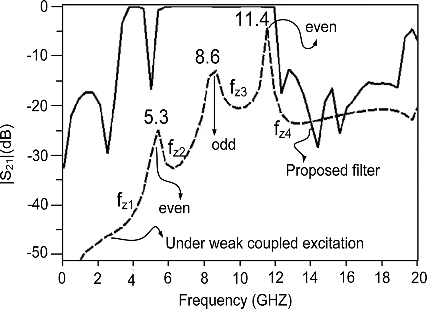
By substituting L 4 = 13.23, L 3 = 3.65, L 2 = 3.40, L 1 = 5.10 in (5), 5.8 and 11.6 GHz are obtained as even mode resonance frequencies. Electromagnetic (EM) simulation in Fig. 6 verifies the above calculations showing one odd mode and two even mode resonance frequencies at 8.63 and 5.38, 11.47 GHz, respectively. So, there is a good agreement between the calculated and simulated resonance frequencies.
 $${Y_{ineven}} = j{Y_4}\displaystyle{{2{Y_4}\tan ({\theta _4}/2) + {Y_3}\tan ({\theta _3})} \over {2{Y_4} - {Y_4}\tan ({\theta _4}/2)\tan ({\theta _3})}},$$
where θ 3 = βL 3, the resonance condition is Y ineven = 0. Thus, at the even mode resonant frequencies for two segments (l 3, l 4) that is showed in Fig. 5(a), it can be derived as
 $$2{Y_4}\tan \left( {\displaystyle{{{\theta _4}} \over 2}} \right) + {Y_3}\tan ({\theta _3}) = 0,$$
 $$2{Y_4}\tan \left( {\displaystyle{{{\theta _4}} \over 2}} \right) = - {Y_3}\tan (\theta {}_3),$$
 $$ - \displaystyle{{2{Y_4}} \over {{Y_3}}} = \tan (\theta {}_3)\cot \left( {\displaystyle{{{\theta _4}} \over 2}} \right).$$
For the special case of Y 3 = 2Y 4
 $$\tan ({\theta _3})\cot \left( {\displaystyle{{{\theta _4}} \over 2}} \right) = - 1.$$
Therefore, the resonance condition for this special case is
 $$\left( {\displaystyle{{{\theta _4}} \over 2}} \right) + ({\theta _3}) = n\pi,$$
or
 $$\displaystyle{{{L_4}} \over 2} + {L_3} = \displaystyle{{n{\lambda _g}} \over 2},$$
 $${\lambda _g} = \displaystyle{c \over {f\sqrt {{\varepsilon _{eff}}}}}.$$
By substituting (3h) into (3g):
 $${L_4} + 2{L_3} = \displaystyle{{nc} \over {f\sqrt {{\varepsilon _{eff}}}}}.$$
The even mode resonant frequencies for the case of Y 3 = 2Y 4 can thus be attained as
 $${f_{even}} = \displaystyle{{nc} \over {({L_4} + 2{L_3})\sqrt {{\varepsilon _{eff}}}}}.$$
In the same way even mode resonance frequency for three and four segments can be calculated as following:
 $${f_{even}} = \displaystyle{{nc} \over {({L_4} + 2{L_3} + 2{L_2})\sqrt {{\varepsilon _{eff}}}}}, $$
 $${f_{even}} = \displaystyle{{nc} \over {({L_4} + 2{L_3} + 2{L_2} + 2{L_1})\sqrt {{\varepsilon _{eff}}}}}. $$
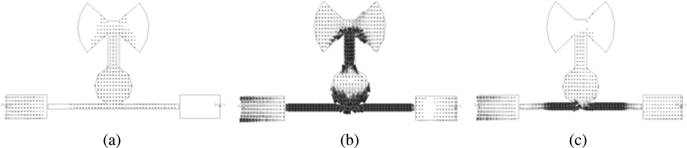
To confirm the above explanations regarding even and odd mode resonance frequencies, current distributions are presented in Fig. 7. As it can be deduced from Fig. 7, θ 4 and (θ 1, θ 2, θ 3, θ 4) contribute to create odd and even mode resonance frequencies, respectively. The difference between current distributions at lower and higher even mode frequencies (Figs 7(a) and 7(b)) relates to the magnitude of insertion loss at these frequencies.

Fig. 6. Simulated frequency response of the proposed UWB filter.

Fig. 7. Electric current distribution of the resonator; (a) lower even mode frequency, (b) higher even mode frequency, (c) odd mode frequency.
B) Transmission Nulls realization
Since transmission zeros occur when S 21 = 0, obtaining them involves calculating the S 21 parameters (Y ino , Yine ) exactly.
 $${S_{21}} = \displaystyle{{{Y_{ino}}{Y_0} - {Y_{ine}}{Y_0}} \over {({Y_0} + {Y_{ino}})({Y_0} + {Y_{ine}})}} = 0, $$
where Y o is the characteristic admittance. The condition of transmission zero frequencies are obtained when Y ino = Y ine . Based on Fig. 5, the input impedance for the even mode can be obtained as following:
 $${z_{ine}} = {z_4}\displaystyle{{{z_a} + j{z_4}\tan ({\theta _4}/2)} \over {{z_4} + j{z_a}\tan ({\theta _4}/2)}},$$
 $${z_a} = 2{z_3}\displaystyle{{{z_b} + j2{z_3}\tan ({\theta _3})} \over {2{z_3} + j{z_b}\tan ({\theta _3})}},$$
 $${z_b} = 2{z_2}\displaystyle{{{z_c} + j2{z_2}\tan ({\theta _2})} \over {2{z_2} + j{z_c}\tan ({\theta _2})}},$$
 $${z_c} = 2{z_1}\displaystyle{1 \over {j\tan ({\theta _1})}}.$$
In the above equations Z 1 corresponds to input impedance of Radial stub. To obtain the value of Z 1 (8) can be used (see Fig. 8) [Reference Wadell15].
 $${z_{in}} = - j\displaystyle{{120\pi h} \over {{r_i}\theta \sqrt {{\varepsilon _{eff}}}}} Ct(\beta {r_i},\beta {r_o}),$$
where
 $$Ct(\beta {r_i},\beta {r_o}) = \displaystyle{{{Y_0}(\beta {r_i}){J_1}(\beta {r_o}) - {J_0}(\beta {r_i}){Y_1}(\beta {r_o})} \over {{J_1}(\beta {r_i}){Y_1}(\beta {r_o}) - {Y_1}(\beta {r_i}){J_1}(\beta {r_o})}},$$
J i (βr) = ith order Bessel function of the first kind having real argument

Fig. 8. Radial stub; (a) series, (b) shunt.
Y i (βr) = ith order Bessel function of the second kind having real argument
 $$\beta = \displaystyle{{2\pi \sqrt {{\varepsilon _{eff}}}} \over {{\lambda _0}}}.$$
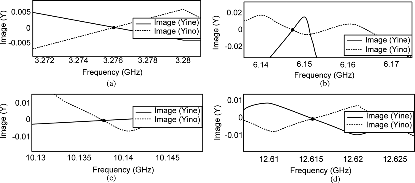
To verify the placement of transmission zeroes, equations (1), (4), (8), (9) have been used to draw two graphs of Y ino and Y ine cutting each other around zero. It can be seen from Fig. 9 that the places of transmission nulls are at around 3.27, 6.15, 10.14, and 12.6 GHz which had already been predicted by EM simulation in Fig. 6. Thus, the places of transmission zeroes are realized by even and odd-mode analysis.

Fig. 9. Location of transmission zeroes by odd and even-mode analysis; (a) fz 1,(b) fz 2, (c) fz 3, (d) fz 4.
IV CHARACTERISTICS OF THE PROPOSED UWB FILTER
A) Controllable notched band
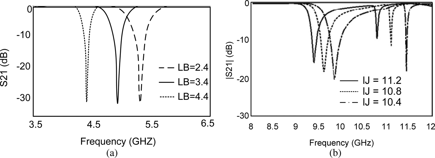
One of the significant features of the proposed UWB filter is related to its ability of sweeping notched band across the passband which makes this structure more applicable for various application. Figure 10(a) shows that the frequency of notched band is mainly controlled by the length of section B in resonator M in Fig. 3(a). Besides the effect of section B on controlling notched band, second and third notched bands can be created and controlled by the length of lJ showed in Fig. 1(a). In the proposed filter, for realizing an ultra-wide passband, the notched band frequency is controlled at 4.99 GHz to suppress IEEE 802. 11a signals.

Fig. 10. Controllable notch band, (a) controlling the first notch band by the length of lB, (b) controlling the second and third notch bands by the length of lJ.
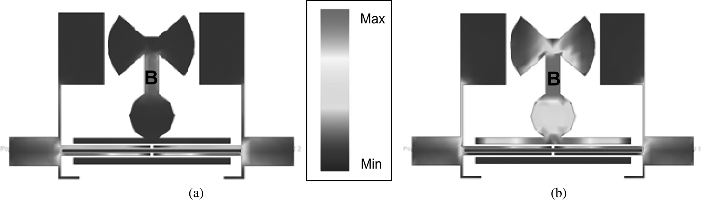
The simulated current densities at center and notch frequencies are shown in Fig. 11. It can be seen from Fig. 11 that section B in Resonator M has the dominant and insignificant effects on the notch and center frequencies, respectively. In the other hands coupled lines have most effects on the center frequency.

Fig. 11. Current density of the proposed filter; (a) at the center frequency (6.39 GHz), (b) at the notched frequency (4.99 GHz).
B) Controllable passband
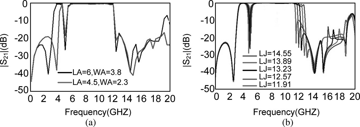
In addition to the adjustable notched band, the passband of the proposed filter can also be controlled by the location of transmission zeroes (Z 1, Z 3). Figure 12(a) shows the dominant effect of lA and WA on the place of Z 1. As it is shown in Fig. 11, by increasing LA and WA, the first transmission zero moves to lower frequencies, causing the center frequency to shift to lower frequencies. This is because by increasing lA and WA the inductance value of the corresponding stub increases which results in a lower resonance frequency. On the other hand, the third transmission zero (Z 3) is controlled by lJ. As it is clear in Fig. 12(b), by lengthening lJ, Z 3 appears at lower frequencies, so the center frequency shifts to lower frequencies. Thus, a controllable center frequency is realized.

Fig. 12. Controllable passband. (a) Controlling lower edge of passband by lA and WA, (b) controlling upper edge of passband by lJ.
V SIMULATION AND EXPERIMENTAL RESULTS
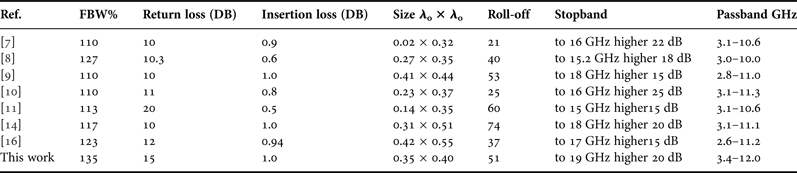
The proposed UWB filter has been fabricated on a substrate with a relative dielectric constant ε r = 2.2, thickness h = 31 mil, and loss tangent tan δ = 0.0009. Fig. 13(a) shows a photograph of the proposed filter. Simulations are done by an EM-simulator (ADS Momentum). The S-parameter is measured by an Agilent network analyzer N5230A. It can be seen from Fig. 13(c) that the 3 dB bandwidth is from 3.40 to 12.00 GHz, a fractional bandwidth (FBW) of 135% which covers the FCC mask. A notch band is generated at 4.99 GHz, with maximum attenuation level of 35 dB. The insertion loss is around 0.5 dB at the lower frequency portion and 1.0 dB at the upper portion. The return loss is greater than 12 dB within the whole passband. The size of the proposed filter is only 14 × 15.6 mm2 which corresponds to 0.35λ 0 × 0.40λ 0. The return loss in the stopband region is very small, indicating negligibly small radiation loss. The measured and simulated group-delay results in Fig. 13(b) exhibit the UWB filter obtains a flat group delay response. The lower transition band from 3 to 3.4 GHz with −3 and −20 dB, respectively, is 0.4 GHz, while the upper transition band equals to 0.28 GHz corresponding to 12 GHz with −3 dB and 12.85 GHz with −20 dB. The deviations of the measurements from the simulations are expected mainly due to the reflections from the connectors and the finite substrate. For comparison, Table 1 provides a breakdown of some UWB filter performances.

Fig. 13. (a) photograph of fabricated UWB filter, (b) group delay, (c) frequency response of the proposed UWB filter, solid line shows measured and dotted line shows simulated results.
Table 1. Copmarision with the reported UWB BPFs.

Note: λ
0 is the free space wavelength of the operating frequency at the center of the passband. Roll-off rate is defined as |α
max
−α
min
|/|f
s
−f
c
| where α
max
is the 20 dB attenuation point and α
min
is 3 dB attenuation point; f
s
is the 20 dB stopband frequency and f
c
is 3 dB cut-off frequency. In the table, average value of the upper and lower roll-offs are reported
 $FBW = ({f_u} - {f_l}) / \sqrt {{f_u}.{f_l}} $
.
$FBW = ({f_u} - {f_l}) / \sqrt {{f_u}.{f_l}} $
.
VI CONCLUSION
A compact UWB filter using RSLR and interdigital coupled lines with 4.99 GHz notched band is presented in this paper. A fully controllable multiple notch band and central frequency are realized with explaining theoretical aspects. Even and odd modes analysis has been employed to yield modal resonance frequencies which contribute to create the passband. On the other hand, the modal analysis is exploited to verify the place of transmission nulls. According to the superior features stating in Table 1 including compact circuit size, high passband selectivity, wide stopband, sharp roll-off, and low insertion loss, the proposed filter is very attractive for the practical applications in modern communication systems.
 Fatemeh Sabaghi was born in Kermanshah, Iran in 1985. She received her B.Sc. degree in Electronic Engineering in 2009 from Islamic Azad University, Kermanshah Branch in Iran and her M.Sc. degree in Electronic Engineering in 2014 from Islamic Azad University, Science and Research Branch in Iran. Her present research interests are RF/Microwave circuit design.
 Gholamreza Karimi was born in Kermanshah, Iran in 1977. He received his B.S., M.S., and Ph.D. degrees in Electrical Engineering from Iran University of Science and Technology (IUST) in 1999, 2001, and 2006, respectively. He is presently an Associate Professor in Electrical Department at Razi University, Kermanshah, since 2007. His research interests include low power Analog and Digital IC design, RF IC design, modeling and simulation of RF mixed signal IC and microwave devices, and artificial intelligence systems.
 Arash Ahmadi received his B.Sc. and M.Sc. degrees in Electronics Engineering from Sharif University of Technology and Tarbiat Modares University, Tehran, Iran, in 1993 and 1997, respectively, and his Ph.D. degree in Electronics from the University of Southampton, UK, in 2008.He was with Razi University, Kermanshah, Iran, as a Faculty Member. From 2008 to 2010, he was a Fellow Researcher with the University of Southampton. He is presently an Associate Professor in the Electrical Engineering Department, Razi University. His present research interests include hardware implementation of signal processing systems, and high-level synthesis.