


I. INTRODUCTION
In recent years, considerable attention has been focused on microwave acoustic filter development because this type of filter provides a good trade-off between performance and size/weight [Reference Aigner1].
Current microwave acoustic filters based on bulk acoustic wave (BAW) resonators are determined to replace conventional surface acoustic wave (SAW) filters since they have now evolved to offer better performance [Reference Aigner1–Reference Loebl, Metzmacher, Milsom, Lok, Van Straten and Tuinhout3]. The core of BAW resonators is the piezoelectric thin film, which is usually aluminium nitride (AlN), zinc oxide (ZnO), or lead zirconate titanate (PZT). AlN is most commonly preferred because it has turned out to be the best compromise between performance and manufacturability. However, in recent years, there has been increasing research activity into resonators based on ZnO and especially PZT, which is the most interesting piezoelectric material due to its excellent properties [Reference Aigner1].
Among the different types of filters that can be synthesized with BAW resonators [Reference Aigner1, Reference Lakin2], electrically connected one-port BAW resonators forming a ladder have always been the mainstay of the technology. This type of filter has an extremely sharp roll-off, but poor stopband rejection. However, in applications where high stopband rejection and no extremely sharp roll-off are required, filters based on two-port BAW resonators (also called stacked crystal filters or SCFs) are a better option.
Nowadays, there are different publications, e.g. [Reference Aigner1, Reference Lakin2, Reference Lakin4, Reference Stokes and Crawford5], where filters based on SCFs have been studied, manufactured, and assessed. However, few systematic design methodologies have been presented, so optimization work is an important part of the design process. For that reason, this paper presents a methodology for designing microwave acoustic filters based on SCFs with either Butterworth or Chebyshev response. As a result of the proposed methodology, a collection of closed-form expressions for the design and analysis of this type of filter can be obtained. As a validation example, the design of a pair of filters for UMTS cellular phone handsets is carried out.
II. ESSENTIAL THEORY ABOUT BAW RESONATORS
A) One-port BAW resonator
A one-port BAW resonator resembles a parallel plate capacitor having piezoelectric material for the dielectric sandwiched between two metal electrodes (Fig. 1(a)) [Reference Aigner1–Reference Loebl, Metzmacher, Milsom, Lok, Van Straten and Tuinhout3]. Its response depends on the material properties, especially piezoelectric properties, and physical dimensions: area, and electrode and piezoelectric thickness.

Fig. 1. One-port BAW resonator: (a) cross section; (b) electrical impedance as a function of frequency. Y-axis in logarithmic scale.
Assuming that spurious modes and other lateral acoustic effects can be spurned, resonator response can be obtained from the physical dimensions and material properties from the well-known Mason model [Reference Mason6]. Figure 1(b) shows the typical electrical impedance Z(w) of a one-port BAW resonator as a function of frequency. This exhibits two close resonant frequencies: f a where the electrical impedance approaches infinity, and f r where it approaches zero. The separation between f a and f r depends on material properties, especially piezoelectric properties. Between these resonant frequencies Z(w) behaves inductively, whereas static capacitive C 0 behavior is found outside of this band.
Since material properties are not a design parameter, the design of this type of resonator entails characterizing only C 0 and f a. The former corresponds to the physical plate capacitance between the electrodes, whereas the frequency f a corresponds to the mechanical resonant frequency of the longitudinal acoustic standing wave generated when an electric field is applied between the electrodes. Both parameters are directly related to the resonator physical dimensions. On the one hand, as in any parallel plate capacitor, C 0 = ɛ0ɛrA/t p is fulfilled, where ɛ0 is the free-space permittivity, ɛr the piezoelectric relative permittivity, A the resonator area, and t p the piezoelectric thickness. On the other hand, the mechanical resonant frequency f a is mainly determined by the piezoelectric thickness, and also by the thickness of the electrodes [Reference Loebl, Metzmacher, Milsom, Lok, Van Straten and Tuinhout3]. In a first approach, without taking electrode thickness into account, the resonant condition is established when the piezoelectric thickness corresponds to a half acoustic wavelength. When electrodes are taken into account, the piezoelectric thickness is lower. In such a case, the thickness of both the piezoelectric and the electrodes can be determined using, for example, the Mason model to obtain the desired f a value.
B) Two-port BAW resonator
A two-port BAW resonator (also called SCF [Reference Aigner1, Reference Lakin2, Reference Lakin4, Reference Stokes and Crawford5]) consists of two one-port BAW resonators tightly coupled acoustically, separated only by a common ground electrode, as shown in Fig. 2(a). In principle, both one-port BAW resonators could be different, but we will assume that they are identical, and therefore that both are characterized by the same C 0 and f a.

Fig. 2. Two-port BAW resonator: (a) cross section; (b) electrical equivalent circuit.
The multiple layers in Fig. 2(a) act as a single resonator with one-pole transmission response. This can be obtained by using the Mason model, but its complexity impedes its use in the design of this type of resonator. For that reason, it is of interest to work with a simpler electrical equivalent circuit (Fig. 2(b)). This narrow-band equivalent circuit is derived from the Mason model without taking electrodes into account [Reference Lakin4, Reference Lakin7]. The final circuit is composed of a series LC resonator (L SCF and C SCF) and two shunt capacitors C 0. These three elements are related through the following expressions [Reference Lakin7]:
and
where C 0 and f a (or the angular frequency w a = 2πf a) are the design parameters of each of the one-port BAW resonators that form part of the SCF, and k t2 is the electromechanical coupling coefficient of the piezoelectric material.
III. FILTER DESIGN METHODOLOGY
The design methodology entails turning the equivalent circuit for an Nth-order bandpass Butterworth/Chebyshev-type filter into an equivalent circuit where the electrical equivalent circuit of N SCFs can be recognized, along with the other necessary elements to obtain the desired Butterworth/Chebyshev response. For the sake of simplicity, the design of a 2nd-order bandpass Butterworth/Chebyshev-type filter will be carried out, but the design methodology can be easily extrapolated for higher orders.
Figure 3(a) shows the equivalent circuit for a 2nd-order bandpass Butterworth/Chebyshev-type filter [Reference Hong and Lancaster8]. It is composed of two series LC resonators and three impedance inverters. It is assumed that the filter is loaded by an arbitrary impedance R, while the source impedance Z 0 is 50 Ω. Both the LC resonators and the load impedance are related to the impedance characteristics of the inverters:
and
where g i, i = 1, 2, 3, are the element values for a 2nd-order Butterworth/Chebyshev lowpass prototype filter, while w 0 = 2πf 0 and Δ are filter specifications: angular center frequency and fractional bandwidth, respectively.

Fig. 3. (a) Equivalent circuit for a 2nd-order bandpass Butterworth/Chebyshev-type filter based on ideal impedance inverters turned into (c) using lumped-element impedance inverters (b).
Figure 3(b) shows a practical implementation of an impedance inverter based on lumped elements [Reference Hong and Lancaster8]. It should be noted that the K parameter of an ideal impedance inverter is not frequency dependent, while the K parameter of a practical impedance inverter is dependent; therefore in lumped-element impedance inverters, K = 1/(w 0C) is assumed. Hence, the limited bandwidth of practical impedance inverters limits how faithfully the desired transfer function is reproduced as the desired filter bandwidth is increased. Therefore, filters designed using impedance inverter theory are best applied to narrow-band filters.
Taking the above explanation into account, the filter equivalent circuit shown in Fig. 3(a) can be turned into the equivalent circuit shown in Fig. 3(c). In this figure, C 1p = −C 01//C 1// − C 12 and C 2p = −C 23//C 2// −C 12, where a//b means a parallel b. Observing this equivalent circuit, the electrical equivalent circuit of two SCFs can be known by intuition, but two challenges arise. On the one hand, there are two negative capacitors. These can be eliminated if ![]() is fulfilled, where
is fulfilled, where ![]() , without the filter transmission response changing significantly. If it is not fulfilled, these can be replaced, in a narrow-band approximation, by inductors
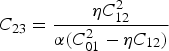
, without the filter transmission response changing significantly. If it is not fulfilled, these can be replaced, in a narrow-band approximation, by inductors ![]() . On the other hand, there is the capacitor C 12, which, as we shall now see, is related to the electrical coupling between both SCFs.
. On the other hand, there is the capacitor C 12, which, as we shall now see, is related to the electrical coupling between both SCFs.
A) Non-controlled electrical coupling between SCFs
Here, we assume that C 12 = C 01 + C 23, and therefore the filter equivalent circuit shown in Fig. 3(c) is turned into the equivalent circuit shown in Fig. 4. This is composed of two SCFs that are electrically connected in cascade and the previously described negative capacitors. It should be noted that in this configuration electrical coupling between resonators is not controlled.

Fig. 4. Filter equivalent circuit composed of two SCFs and two negative capacitors.
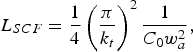
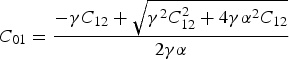
The next step is to take into account the connections between elements that form part of the electrical equivalent circuit of an SCF, shown in (1, 2). Using these expressions, the design parameters of the first SCF (C 01 and w a1) can be obtained:
and
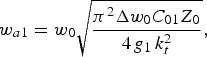
where ![]() , with
, with ![]() , and
, and ![]() . The design parameters of the second SCF (C 23 and w a2) are:
. The design parameters of the second SCF (C 23 and w a2) are:
and
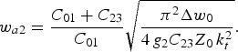
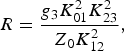
It should be noted that once C 01 and C 23 have been obtained, then C 12 is automatically determined (C 12 = C 01 + C 23), which means that the load impedance R is also determined by means of (6), which can easily be rewritten as:
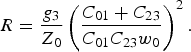
It is important to observe that if ϒ < 0 in (7), the results provided by (7–11) are complex numbers, which is not physically possible. To avoid this, it is necessary that:
which implies that 1.5% > Δ > 128%, assuming that g 1 and g 2 are the element values for a 2nd-order Chebyshev lowpass prototype filter (passband ripple 3 dB), and AlN is used as a piezoelectric material (k t2 = 5.7% [Reference Lakin2]). Since it is not possible to design filters with Δ > 128% because the narrow-band approximations used throughout this work would not work properly, this approach is therefore only valid to Δ < 1.5%.
Figure 5 shows the results provided by (7–11) as a function of fractional bandwidth Δ for a filter with Chebyshev response (f 0 = 1950 MHz and passband ripple 3 dB), assuming that AlN is used as a piezoelectric material. This figure shows that only filters with Δ from about 1 to 1.5% can be manufactured with current technology, which limits the benefit of this approach. In order to extend the margin of possible fractional bandwidths, the electrical coupling between resonators will be controlled by means of a reactive element, as we shall see in the following section.

Fig. 5. Design parameters as a function of fractional bandwidth for a filter with Chebyshev response (f 0 = 1950 MHz and passband ripple 3 dB), assuming that AlN is used as a piezoelectric material. (a), (b), and (c) show the results provided by (7–11) using ⊕ in (7), while (d), (e), and (f) show the results using ⊖. In (a) and (d), the Y-axis is in logarithmic scale.
Finally, it is important to point out that as this approach only serves to design narrow-band filters, the negative capacitors can be eliminated because ![]() is always fulfilled, where C ij = C 01, C 23. In those cases, the resulting filter is only composed of two SCFs that are electrically connected in cascade, and it is loaded by an impedance that is, generally, different from Z 0.
is always fulfilled, where C ij = C 01, C 23. In those cases, the resulting filter is only composed of two SCFs that are electrically connected in cascade, and it is loaded by an impedance that is, generally, different from Z 0.
B) Controlled electrical coupling between SCFs
In the following approach, the electrical coupling between resonators will be controlled by means of a shunt reactive element. For the sake of simplicity, we will assume that this is a capacitor C c; therefore, the filter equivalent circuit shown in Fig. 3(c) can be turned into the equivalent circuit shown in Fig. 6, where ![]() . This filter equivalent circuit is composed of a cascade of two SCFs, a shunt coupling capacitor C c, and two series negative capacitors that as in the previous case can be eliminated for narrow bandwidths.
. This filter equivalent circuit is composed of a cascade of two SCFs, a shunt coupling capacitor C c, and two series negative capacitors that as in the previous case can be eliminated for narrow bandwidths.

Fig. 6. Filter equivalent circuit composed of two SCFs, a shunt coupling capacitor, and two negative capacitors.
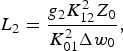
Taking into account the connections between the elements that form part of the electrical equivalent circuit of an SCF, shown in (1, 2), the design parameters of the first SCF (C 01 and w a1) can be obtained:
and
where ![]() , while the design parameters (C 23 and w a2) of the second SCF are:
, while the design parameters (C 23 and w a2) of the second SCF are:
and
It should be noted that, unlike the previous case, two pairs of solutions are not there. However, multiple different solutions can be obtained as a function of the chosen C 12 value, which can be considered to be a degree of freedom.
Once C 12 has been chosen, and C 01 and C 23 determined, it is straightforward of obtaining the coupling capacitance C c = C 12 − C 01 − C 23, and the load impedance R by means of (6), which can, in such a case, be easily rewritten as:
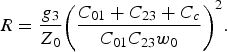
An interesting case is when the chosen ![]() value provides that
value provides that ![]() since in this case both SCFs are the same, i.e.
since in this case both SCFs are the same, i.e. ![]() and
and ![]() . Figure 7 shows the design parameters of each SCF (C 0 and f a ) along with the coupling capacitor C c as a function of fractional bandwidth Δ for a filter with Chebyshev response (f 0 = 1950 MHz and passband ripple 3 dB), assuming that AlN is used as a piezoelectric material.
. Figure 7 shows the design parameters of each SCF (C 0 and f a ) along with the coupling capacitor C c as a function of fractional bandwidth Δ for a filter with Chebyshev response (f 0 = 1950 MHz and passband ripple 3 dB), assuming that AlN is used as a piezoelectric material.

Fig. 7. Design parameters as a function of fractional bandwidth for a filter with Chebyshev response (f 0 = 1950 MHz and passband ripple 3 dB) and loaded by an impedance R = Z 0, assuming that AlN is used as a piezoelectric material.
This figure shows that it is relatively easy to manufacture filters with Δ > 0.7% with current technology. Narrower bandwidths can be achieved if R ≠ Z 0, and therefore both resonators will be different. It should be noted that ![]() for
for ![]() . In those cases, the capacitor is replaced by an inductor
. In those cases, the capacitor is replaced by an inductor ![]() , whose value is represented in the inset of the figure. Bandwidths about 1.5% are not possible because either very low coupling capacitors or very high coupling inductors are necessary. Besides, it is important to point out that for Δ from about 3.5%, as the bandwidth is higher, the filter transmission response is worse in comparison to the theoretical one due to the narrow-band approximations carried out.
, whose value is represented in the inset of the figure. Bandwidths about 1.5% are not possible because either very low coupling capacitors or very high coupling inductors are necessary. Besides, it is important to point out that for Δ from about 3.5%, as the bandwidth is higher, the filter transmission response is worse in comparison to the theoretical one due to the narrow-band approximations carried out.
In short, the introduction of a coupling reactive element makes it possible to design the same bandwidths as in the first approach, but loading the filter with the desired impedance. Besides, this approach makes it possible to design filters with narrower and especially wider bandwidths, loading the filter with the desired impedance. However, the introduction of this element offers two drawbacks in that it increases the complexity and size of the filter, and adds new losses.
IV. PREDICTED PERFORMANCE AND DISCUSSION
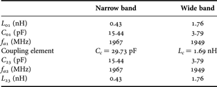
In order to validate the presented work, the design of a pair of filters for UMTS cellular phone handsets will be carried out. Both filters will be designed with 2nd-order Chebyshev response (f 0 = 1950 MHz and passband ripple 3 dB). As regards the bandwidth BW, one will be designed for narrow-band operation BW = 15 MHz (Δ = 0.77%) and the other for wide-band operation BW = 60 MHz (Δ = 3.08%).
Figure 8 shows a schematic illustration of the designed filters, where it is observed that a coupling reactive element and a load impedance R = Z 0 are used. Table 1 shows the design parameters of each filter. These have been obtained using the work presented in Section III, assuming that AlN is used as a piezoelectric material.

Fig. 8. Schematic illustration of a 2nd-order Chebyshev-response filter composed of two SCFs, two inductors in series, and one coupling reactive element.
Table 1. Filter design parameters.
Figures 9 and 10 show the simulated lossless transmission response of each designed filter along with the theoretical one. The designed filters were simulated using the Mason model implemented in a commercial microwave design simulator (Advanced Design System). These figures show that in the narrow-band case the agreement in both responses is excellent, while in the wide-band case the agreement is slightly poorer, but in-band the agreement is good. This is due to the narrow-band approximations carried out. Figure 9 also shows that, in the narrow-band case, the inductors L 01 and L 23 can be eliminated without the transmission response changing significantly.

Fig. 9. Simulated lossless narrow-band (BW = 15 MHz) filter transmission response: designed filter (continuous line), theoretical response (dashed line), and designed filter without inductors in series (circles).

Fig. 10. Simulated wide-band (BW = 60 MHz) filter transmission response: designed filter taking (dotted line) and without taking (continuous line) losses into account, and theoretical response (dashed line).
A priori, the use of inductors/capacitors involves two drawbacks: The losses added by these, and the increase in filter size and complexity. As regards losses, Fig. 10 also shows the wide-band (BW = 60 MHz) filter transmission response taking losses into account. It is assumed that the quality factor of each resonator is 1000 [Reference Shirakawa, Pham, Jarry and Kerhervé9], while the quality factor of each of the three inductors is 32 [Reference Rais and Ayazi10]. This figure shows that, in such a case, the maximum insertion loss is about 2 dB. Inductors with high-quality factors ranging from 30 to 80 at 2 GHz can been obtained [Reference Rais and Ayazi10]. For example, by using inductors with a quality factor of 60, the maximum insertion loss is reduced by 0.5 dB.
As regards the increase in size and complexity, it should be noted that while the area of each SCF for the wide-band filter is about 347 × 347 µm2, each of the three inductors is of a similar area: 400 × 400 µm2 [Reference Rais and Ayazi10]. Therefore, the increase in filter size is the main drawback. However, in the design of filters with narrower bandwidths, this drawback is less important since inductors in series can be eliminated.
V. CONCLUSION
A methodology for designing microwave acoustic filters, based on stacked crystal filters, with either Butterworth or Chebyshev response has been presented. The proposed methodology makes it possible to design this type of filter without any optimization work, and, moreover, closed-form expressions for its design and analysis can be obtained as a function of filter specifications.
As a validation example, the design of a pair of filters for UMTS cellular phone handsets has been carried out. The transmission response of the designed filters has been obtained using the Mason model. The different simulations carried out show the good agreement between the transmission response of the designed filters and the theoretical response. As regards experimental validation, due to the shortage of data in papers where filters with a similar structure and response are manufactured and measured, it has not been possible to validate the presented work against the published work of other authors.
ACKNOWLEDGEMENTS
This work was supported by the Spanish Comisión Interministerial de Ciencia y Tecnología (CICYT) del Ministerio de Educación y Ciencia and FEDER funds through grant TEC2006-13248-C04-01/TCM.
 Óscar Menéndez was born in Barcelona, Spain, in 1977. He received Telecommunication Engineering and Ph.D. degrees from the Universitat Politècnica de Catalunya (UPC) in 2001 and 2005, respectively. From 2001 to 2005, he was a member of the Advanced Materials and Technologies for Communications Group of the UPC. Since 2002 he has been a Full Professor at the Universitat Autònoma de Barcelona, where he is a member of the Antenna and Microwave Systems Group. His primary research lines include microwave devices and systems, and BAW resonators and filters. He has published more than 12 technical papers.
 Pedro de Paco was born in Badalona, Spain. He received an M.S. degree in Telecommunication Engineering in 1997 and a Ph.D. degree in 2003 from the Universitat Politècnica de Catalunya (UPC). In 1998, he joined the Electromagnetic and Photonics Engineering Group (EEF-UPC) with a grant in a joint activity related to the European space mission Planck. From 1999 he was a member of the EEF Group and from 2003 to 2004 he has been an associate professor at the UPC. Since 2004 he has been a Lecturing Professor at the Universitat Autònoma de Barcelona. His current areas of interest include: hybrid and monolithic technologies, device modeling and emerging technologies for device miniaturization.
 Joan Gemio was born in Barcelona, Spain, in 1984. He received a Telecommunication Engineering degree in 2007 from the Universitat Autònoma de Barcelona (UAB). Since 2007 he has been a member of the Antenna and Microwave Systems Group at the UAB. His research interests include antenna and microwave systems. He was the recipient of the 2004/05 prize for the best national academic record in the Technical Telecommunication Engineering degree.
 Jordi Verdú was born in Sabadell, Spain, in 1980. He received a Telecommunication Engineering degree in 2006 from the Universitat Autònoma de Barcelona (UAB). Since 2006 he has been a member of the Antenna and Microwave Systems Group at the UAB. His research interests include microwave and acoustic devices and systems.
 Edén Corrales was born in Sabadell, Spain, in 1984. He received a Telecommunication Engineering degree in 2007 from the Universitat Autònoma de Barcelona (UAB). Since 2007 he has been a member of the Antenna and Microwave Systems Group at the UAB. His research interests include microwave devices and systems, especially BAW resonators and filters.


