I. INTRODUCTION
Modern wireless communication devices are required to support multi-standards and multi-services operating at different frequency bands. Thus, the designing of multi-band antenna has been the focus of research in recent years as multi-band antennas are able to resonate over several bands which leads to integration of different communication standards operating at different and nearby frequency bands in a single device. Multi-band antennas can be thought of as an intermediate solution combining simplicity and multi-frequency operation. Some wireless communication applications of antennas are required to simultaneously operate for Wireless Local Area Network (WLAN) and Worldwide Interoperability for Microwave Access (WiMAX) technology. The operating bands for these technologies as assigned by IEEE 802.11 are 2.4 GHz (2.4–2.484 GHz), 5.2/5.8 GHz (5.15–5.35 GHz/5.725–5.825 GHz), and 2.5/3.5/5.5 GHz (2.5–2.69/3.4–3.69/5.25–5.85 GHz). Several antenna configurations have been suggested for WLAN and WiMAX bands in recent years, such as a dual-band antenna [Reference He, Hong, Xiong and Qishan1], asymmetric M-shaped triple-band antenna [Reference Peng, Ruan and Wu2], a compact triple-band microstrip slot antenna [Reference Dang, Lei, Xie, Ning and Fan3], miniaturized triple-band antenna with a defected ground plane [Reference Pei, Wang, Gao and Leng4], and dual wideband antenna [Reference Chu and Ye5]. In [Reference Yldrm, Baaran and Türetken6], a compact planar dielectric-loaded, multiple-band antenna is presented. A frequency agile triple-band microstrip antenna using defected ground structure (DGS) for WLAN/WiMAX application is presented in [Reference Joshi, Gautam and Upadhyay7]. In [Reference Hu, Yin, Fei and Yang8], an antenna with symmetrical L-strips is presented. This antenna is composed of a square slot, a pair of L-strips, and a monopole radiator fed with coplanar waveguide (CPW) feed line which makes its structure complex. Furthermore, a H-shaped multi-band antenna is presented in [Reference Chang and Kiang9]. A planar inverted-F antenna in conjunction with a parasitic element is reported in [Reference Wang and Zheng10]. In [Reference Zhai, Ma, Han and Liang11], compact triple-band printed antenna is reported that consists of three simple circular-arc-shaped strips. It has complex structure which limits its practical application. A CPW-fed tri-band printed antenna with meandering split-ring slot for WLAN/WiMAX applications is presented in [Reference Liu, Zou, Xie, Liu and Sun12]. In [Reference Huang, Li and Zhao13], a square ring, an open ended stub, and an inverted T-shaped stub are used to achieve triple-band operation. The microstrip-fed antenna which consists of a rectangular patch, dual inverted L-shaped strips, and a defected ground is proposed for WLAN/WiMAX band [Reference Wang, Yin, Yang, Zhang and Xie14].
In this paper, a compact triple-band antenna with DGS for WLAN and WiMAX applications is proposed. It provides three impedance bandwidths of 2.39–2.51 GHz (70 MHz), 3.15–3.91 (760 MHz), and 4.91–6.08 GHz (1170 MHz), respectively. The proposed antenna is compact in size (20 × 30 mm2) and simple in configuration. A prototype of the antenna has been constructed and demonstrates satisfactory performance. Table 1 illustrates the useful fact about the antennas recently proposed for WiMAX/WLAN applications. From the Table 1, it is evident that the proposed antenna has smallest size as compared with the other mentioned antennas with a sufficient bandwidth at all three bands to cover entire WLAN and WiMAX bands. Details of antenna design, the simulated and measured results are presented and discussed in the following sections.
Table 1. Performance comparison of the proposed antenna with other reported antennas.

II. ANTENNA DESIGN AND SIMULATION APPROACH
The schematic configuration of the proposed microstrip-fed planar monopole antenna for triple-band operation is shown in Fig. 1. The slot antenna is printed on a FR4 substrate with a thickness of 1.6 mm and a relative permittivity of 4.4 and loss tangent 0.02. For the purpose of compactness, the width of the radiator is set to be the same as that of the microstip feed line. The antenna consists of a rectangular radiating patch with an inverted L-shaped slot of length L p1 and width W p2. The conventional solid ground plane is converted into DGS by cutting rectangular slots to excite lower and higher resonant bands and to achieve compactness. The antenna is fed with 3 mm wide microstrip line to achieve 50 Ω-characteristic impedance.

Fig. 1. Schematic configuration of the proposed inverted L-slot triple-band antenna.
Figure 2 illustrates the return loss of rectangular patch radiator and DGS. It is clearly evident from the Figure (curve (ii)) that by cutting three slots in a half solid ground, two resonant modes are excited, one at same resonant mode of the original ground plane and other resonant mode at the higher frequency due to DGS with good impedance matching in both the bands. Furthermore, curve (iii) illustrates that another resonant band at low frequency is also excited due to the insertion of the inverted L-slot in the radiating patch. Therefore, by cutting these rectangular slots in the ground plane (i.e. making DGS) and inverted L-slot in the rectangular radiating patch, three resonances will be excited with a good impedance matching.

Fig. 2. Simulated return loss against frequency for the various antenna configurations.
To clarify the phenomenon behind the excitation of triple-bands in inverted L-slot antenna with DGS, the surface electrical currents of the proposed antenna at three frequencies 2.5, 3.5, and 5.5 GHz are shown in Fig. 3. It is evident from the Fig. 3(b) that the lower band around 2.5 GHz is excited mainly due to the inverted L-slot. Fig. 3(c) and 3(d) reveals that the other two bands are excited mainly due to DGS.

Fig. 3. Simulated surface current distributions at various frequencies of the proposed antenna.
III. PARAMETRIC STUDY
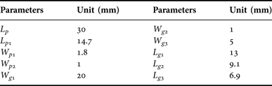
The final antenna design is achieved by tuning the length, width, and the slot dimensions of the radiating patch and the DGS. To understand the influence of these parameters on the antenna performance, a parametric study on the triple-band antenna is carried out. From the parametric study, the optimum value for each parameter of the proposed antenna is obtained as listed in Table 2. Ansoft “High Frequency Simulation Structure” (HFSS) simulator [15] is used to perform the parametric study of the design.
Table 2. Design parameters of the proposed antenna.

A) Variation of patch parameters
The dimensions of patch slot are critical parameters in determining the sensitivity of impedance matching at lower resonant band. The effect of the parameter L p1, length of the inverted L-slot, on the magnitude of the reflection coefficient of the antenna is depicted in Fig. 4 as L p1 is varied from 12.7 to 16.7 mm. It can be seen from the Fig. 4 that the lower frequency band shifts toward lower frequency as L p1 is increased from 12.7 to 14.7 mm. It is also found that L p1 slightly affects the middle band while the third resonant band almost remains unchanged. Thus, the results indicate that the optimum value of L p1 is 14.7 mm. The effects of slot width W p2 on the impedance bandwidth and reflection coefficient are depicted in Fig. 5. It can be observed from the simulation results that as the value of W p2 increases from 0.5 to 2 mm, the lower band shifts toward lower frequency with a degradation in impedance matching with minimum effect on the middle and higher bands. The antenna shows dual band operation with furthermore increase in the value of W p2. Thus, the value of W p2 is chosen 1 mm as optimum to excite the lower band 2.5 GHz.

Fig. 4. Simulated return loss against frequency for the proposed antenna with various L p1 other parameters are the same as listed in Table 2.

Fig. 5. Simulated return loss against frequency for the triple-band antenna with various W p2 other parameters are the same as listed in Table 2.
B) Variation of ground parameters
Keeping all the dimensions invariant, the simulated return loss for different values of ground length L g1 is depicted in Fig. 6. The impedance bandwidth of the third band is improved with the length L g1. With L g1 = 11 mm only two resonating bands are formed. Furthermore, at the length = 12 mm, three resonating bands are obtained but third band has very less bandwidth. Finally, at 13 mm value of L g1, all desired three resonating bands are obtained and further increase in length reduces the bandwidth of the second band and dual resonating bands are obtained. Hence, the value of L g1 = 13 mm is chosen as an optimum. The effect of length L g2 of the ground plane on the performance of antenna is depicted in Fig. 7. It is keenly observed that as the length is varied from 7.1 to 9.1 mm, impedance bandwidth of second and third resonating bands are greatly increased. Furthermore, increase in length increases the bandwidth of the third band but simultaneously decreases bandwidth of second resonating band. Thus, the optimum value for the length L g2 of the ground plane is chosen as 9.1 mm.

Fig. 6. Simulated return loss against frequency for the triple-band antenna with various L g1 other parameters are the same as listed in Table 2.

Fig. 7. Simulated return loss against frequency for the triple-band antenna with various L g2 other parameters are the same as listed in Table 2.
IV. EXPERIMENTAL RESULTS AND DISCUSSION
To verify the design, antenna is practically fabricated on epoxy FR4 substrate, the photograph of the fabricated antenna is illustrated in Fig. 3(a). An Agilent N5230A vector network analyser is used to measure the electrical performance of the proposed antenna such as return loss, radiation patterns. Measured and simulated results for the return loss of the antenna are shown in Fig. 8 that shows a good agreement between simulation and measurement for the relative bandwidth. It is found that proposed design shows triple-band operation i.e. first band from 2.39 to 2.51 GHz, second band from 3.15 to 3.91 GHz, and third band from 4.91 to 6.08 GHz which evidently covers entire WiMAX (2.5/5.8/3.5-GHz) and WLAN (2.4/5.2/5.8-GHz) bands.

Fig. 8. Measured and simulated results of the return loss of proposed triple-band antenna.
Gain and efficiency variations with the frequency are shown in Fig. 9. It is found that the gain remains consistent through all three bands and varies from 1.9 to 6 dB. It is also observed from the Fig. 9 that the radiation efficiency of the antenna is varied from 60 to 90%. Both gain and efficiency drop drastically for frequencies other than resonant bands. Figure 10(a)–10(c) shows the 2D far-field radiation patterns in the H- and E-planes at sampling frequencies of 2.5, 3.5, and 5.5 GHz, respectively. In these figures, good omni-directional radiation characteristics are observed. However, the measured result shows some deviation from the simulated result; this may be due to fabrication imperfection or because measurement is carried out in the scattering environment.

Fig. 9. Gain and Efficiency of proposed compact triple-band antenna.

Fig. 10. Measured and simulated radiation patterns at (a) 2.5 GHz, (b) 3.5 GHz, and (c) 5.5 GHz resonance frequencies. Measured – and Simulated –.
V. CONCLUSION
A compact triple-band planar antenna with an inverted L-slot on the radiating patch with DGS is presented for WLAN/WiMAX applications. The antenna generates three resonant bands to integrate WiMAX and WLAN communication standards in a single device. The measured and simulated results show that the omni-directional radiation characteristics and the impedance bandwidth are very suitable for the WLAN and WiMAX applications. The proposed antenna provides sufficiently large band width in all three frequency bands with compact and simple structure.
 Alaknanda Kunwar was born in Chamoli District of Uttarakhand state of India, in May 25, 1986. She received B.Tech degree in Electronics and communication engineering and M.Tech. degree in digital signal processing from G. B. Pant Engineering College Pauri (Uttarakhand) in 2010 and 2013, respectively. She has published many research papers in reputed journals/conferences like IEEE, etc. Her main research interests are design and optimization of circularly polarized antennas, RFID, and antennas for WLAN/WIMAX applications, etc.
 Anil Kumar Gautam was born in NOIDA, Uttar Pradesh, India. He received the B.E. degree in Electronics and Communication Engineering from Kumaon Engineering College, Almora, India and the Ph.D. degree in Electronic Engineering from Indian Institute of Technology, Banaras Hindu University, Varanasi, India, in 1999 and 2007, respectively. He joined the Department of Electronics and Communication Engineering, G. B. Pant Engineering College, Pauri Garhwal, India, in 2000, as an Assistant Professor and he has been an Associate Professor there since 2009. Dr. Gautam is an active member of the Board of study, Academic council, and many other academic committees of GBPEC, Pauri. He is also a member of the BOS of HNB Garhwal Central University, INDIA and Uttarakhand Technical University, Dehradun, INDIA. He is nominated as Nodal Officer, TSP, and SCSP Grants by Government of Uttarakhand and executed several projects under these grants. He has supervised 15 M.Tech. and one Ph.D. Thesis and currently supervising nine Ph.D. Theses in the area of Microstrip antenna. He is the author/co-author of more than 70 research papers published in the refereed international journals and conferences such as IEEE, Microwave and optical Technology Letters, Springer, etc. He is the author of 13 books in the field of Electronics Engineering, Digital Electronics, Antenna and Microwave Engineering. He is a member of IEEE (USA) and many other technical societies. He is also in reviewers panel of IEEE, Transaction on Antenna and Propagation, IEEE, Antenna and Wave Propagation Letters, IET Microwaves, Antennas and Propagation, Personal and wireless communication, Springer, International Journal of Electronics, International Journal of Microwave and Wireless Technologies, International Journal of Antenna and Propagation, etc. His main research interests are in design and Modeling of Active Microstrip Antenna, Microstrip antennas with Defected Ground Structure, Ultra wide bandwidth antennas, and reconfigurable antennas, reconfiguration antenna array, circular polarized antenna, etc.
 Binod Kumar Kanaujia is currently working as Associate Professor in the Department of Electronics and Communication Engineering in Ambedkar Institute of Advanced Communication Technologies & Research (formerly Ambedkar Institute of Technology), Geeta Colony, Delhi. Dr. Kanaujia joined this institute as Assistant Professor in 2008 through selection by Union Public Service Commission, New Delhi, India and served on various key portfolios i.e. Head of Department, In-charge Central Library, Head of Office, etc. Before joining this institute he had served in the M.J.P. Rohilkhand University, Bareilly, India as Reader in the Department of Electronics & Communication Engineering and also as Head of the Department. He has been an active member of Academic Council and Executive Council of the M.J.P. Rohilkhand University and played a vital role in academic reforms. Prior to his career in academics, he has worked as Executive Engineer in the R & D division of M/s UPTRON India Ltd. Dr. Kanaujia had completed his B.Tech. in Electronics Engineering from KNIT Sultanpur, India in 1994. He did his M.Tech. and Ph.D. in 1998 and 2004, respectively from Department of Electronics Engineering, Indian Institute of Technology Banaras Hindu University, Varanasi, India. He has been awarded Junior Research Fellowship by UGC Delhi in the year 2001–2002 for his outstanding work in Electronics field. He has keen research interest in design and modeling of microstrip antenna, dielectric resonator antenna, left handed metamaterial microstrip antenna, shorted microstrip antenna, ultra wideband antennas, reconfigurable, and circular polarized antenna for wireless communication. He has been credited to publish more than 105 research papers with more than 200 citations with h-index of 10 in peer-reviewed journals and conferences. He had supervised 45 M.Tech. and three Ph.D. research scholars in the field of microwave engineering. He is a reviewer of several journals of international repute i.e. IET Microwaves, Antennas and Propagation, IEEE Antennas and Wireless Propagation Letters, Wireless Personal Communications, Journal of Electromagnetic Wave and Application, Indian Journal of Radio and Space Physics, IETE Technical Review, International Journal of Electronics, International Journal of Engineering Science, IEEE Transactions on Antennas and Propagation, AEU-International Journal of Electronics and Communication, International Journal of Microwave and Wireless Technologies, etc. Dr. Kanaujia had successfully executed four research projects sponsored by several agencies of Government of India i.e. DRDO, DST, AICTE, and ISRO. He is also a member of several academic and professional bodies i.e. IEEE, Institution of Engineers (India), Indian Society for Technical Education, and The Institute of Electronics and Telecommunication Engineers of India.