


I. INTRODUCTION
United Monolithic Semiconductors (UMS) has been a major European player in the GaAs technology over the past 10 years. Extending its technology portfolio to include GaN seems to be a logical step forward. However, such a move for a company its size requires a very high level of confidence in the potential of this new technology and its chance of success. This resulted in a rather conservative approach at the beginning, mostly involving evaluation and observation of the development done at partner institutes in the first phase. Once it became clear that GaN would become the technology of choice for many future applications and after securing the necessary financial and technical support, the second phase of active development of an internal production capability. The comparatively late start of this second phase, in particular in comparison to major competitors outside Europe, could be compensated by very close collaborations with partners close or at the current state-of-the-art. Indeed, a large European community has focused in the last decade on the research and development of GaN technology and devices to reach a level excellence comparable to the rest of the world [Reference Blanck, Splettstößer and Floriot1]. The present paper will summarize the current status achieved and illustrate it with a few representative examples. Aspects covering material, devices, and circuits will be addressed in the following sections.
II. Material
A) Substrate
When starting the development actives inside UMS a key issue was to define the most appropriate substrate for GaN. Although SiC seemed clearly to be best choice in terms of performance, allowing very high-power density thanks to its high thermal conductivity, it was plagued by various key problems. In particular, substrate size, cost, and defect density seemed overwhelming. On the other hand, Si looked like a good alternative with many advantages. Finally, the choice was made to focus on SiC in order to capitalize on the best performance potential. Over the last few years the early limitations of SiC could be significantly relaxed, in particular, substrate size and defect density. UMS baseline relies on 3-in. material, which has become the current de-facto standard, but the fab can accommodate 4-in. and the transfer will be made when the quality and availability are satisfactory.
In parallel, activities are still running to evaluate alternative solutions. Interesting results have been obtained on hybrids substrates in an attempt to reduce cost and increase wafer dimensions without impacting performances [2, Reference Defrance3].
B) Epitaxy
Like for its GaAs activity UMS relies on commercial suppliers to provide the epitaxy of the AlGaN/GaN layers. This allows the best compromise cost/quality and has already proven to be a very effective solution. Material of excellent quality is available from sources both inside and outside Europe. Aside from the usual uniformity and reproducibility of sheet resistance and carrier concentration, special care has been taken to choose an epitaxy material providing adequate buffer isolation. This is essential for power applications at high bias voltage and using devices with short gate-length.
III. Process
A) Overview
Figure 1 shows the UMS' GaN technology roadmap. In a first phase two families are being developed to address application up to 6 GHz (GH50) and 20 GHz (GH25), respectively. In a second phase two additional families are planned dedicated to higher frequencies (GH15) and specific applications (Switch Mode).
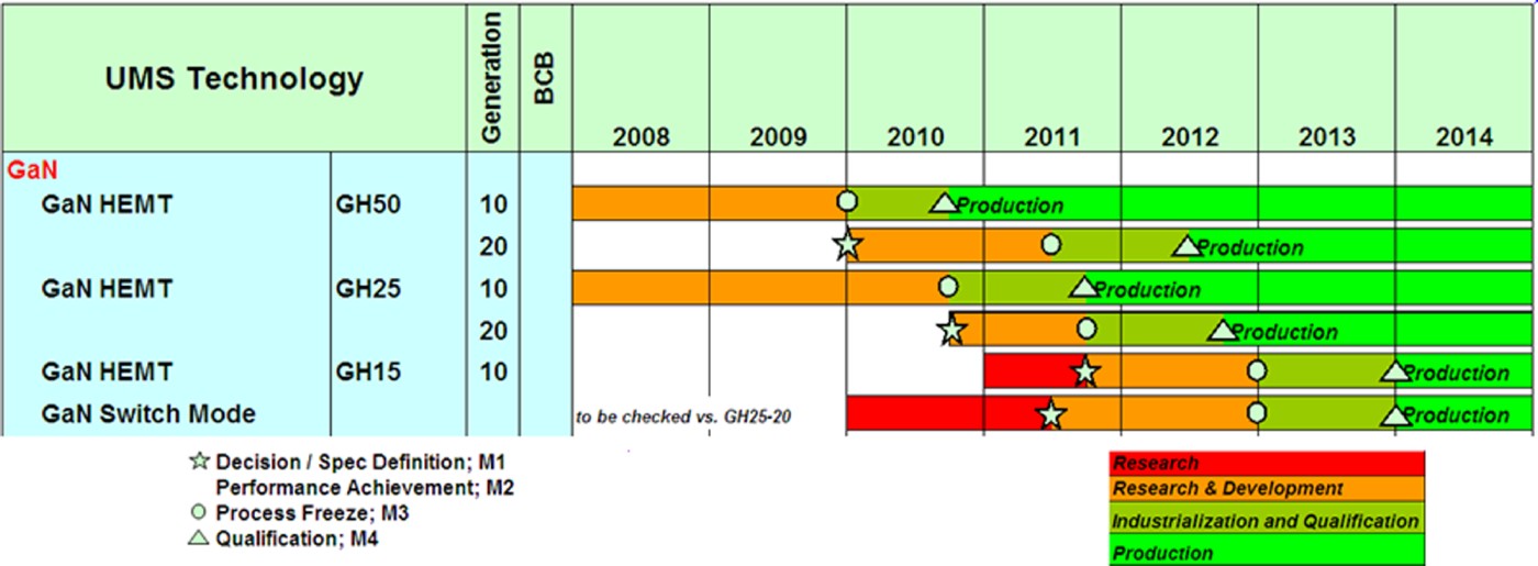
Fig. 1. GaN technology roadmap.
The first technology (GH50) is based on a half-micron transistor and is dedicated to the fabrication of large-periphery power bars. This is the most advanced and a first generation is scheduled to be qualified in 2010. A second generation is planned with improved performances and features. One key feature of this technology is to allow safe operation at 50 V drain bias, which is fundamental to make best use the intrinsic physical properties of GaN.
The second technology (GH25) is based on a quarter-micron transistor and offers a full MMIC capability. A first generation is scheduled to be qualified in 2011 and will also be followed by a second generation. However, first demonstrators have already been designed and fabricated to validate its potential (see Section V).
B) Process
Both GH50 and GH25 technologies strongly rely on UMS GaAs experience and use, wherever possible, identical modules. In particular, the gate module is based in both cases on an SiN-assisted gate-foot definition identical to their GaAs counterparts. This provides excellent process control and reproducibility. The etching process and metal stack were optimized to achieve the best performance and stability [Reference Jung4]. The Ohmic contact has been optimized through several iterations in order to reach appropriate electrical and morphological properties. The improved morphology of the Ohmic contact can be seen in Fig. 2. Good electrical results are obtained for a wide range of epitaxy suppliers and specifications (see Fig. 3). Both technologies integrate a full backside process including via holes and a final wafer thickness of 100 µm. The current via hole process is based on a conventional dry etching step, but an alternative approach using laser drilling has also been successfully evaluated [Reference Stieglauer, Bödege, Öttlin, Ilgen, Blanck and Behammer5].

Fig. 2. Ohmic contact cross-section: left: first generation; right: current generation.

Fig. 3. Ohmic contact resistivity trend chart versus epitaxy supplier and specification.
C) Device physical simulations
In order to optimize the process and device performances, it is necessary to perform an important number of variations and iterations. Although experimental results are still the foundation of any technology development, it is often not possible, for time and cost reasons, to actually realize experimentally all possible cases. To compensate this UMS made extensive use of physical device simulations.
As an example we show here how we used the device simulation tool Silvaco ATLAS [6] to assess the origin of gate leakage current in the devices. This is of interest because of several reasons. Leakage currents in high electron-mobility transistor (HEMT) devices are known to limit the power added efficiency (PAE) for power devices but have also severe impact on their noise performance [Reference Sanabria, Chakraborty, Xu, Rodwell, Mishra and York7].
1) Design of experiment
Device fabrication utilizing a dielectric-assisted gate process is widely used in state-of-the-art III-V technology and so it was during the processing of these devices. During the processing the Schottky interface is exposed to fluorine-based plasma baring the risk of heavy plasma damage which can be the root cause of excessive gate leakage. Therefore, a high density of donor-like traps was introduced below the gate contact and a simple Schottky tunneling model was applied. For more detailed information on the model the authors would like to refer to [Reference Hosch, Behtash, Thorpe, Blanck, Riepe and Schumacher8].
2) Simulation results
Figure 4 shows the dependence of the leakage current of the gate-source diode on the trap density. It can be seen that a trap density of n T > 1 × 1018 cm−3 is needed to achieve an effect on the gate leakage level. However, high trap densities can vary the gate leakage level over five orders of magnitude.

Fig. 4. Simulation results showing the dependence of gate leakage on traps density.
Figure 5 depicts the simulation results on the temperature dependence of the gate leakage. A strong increase of the forward Schottky current is observed and the gate leakage level can vary by another three orders of magnitude just by increasing the ambient temperature. All these phenomena are in good agreement with what is observed in experiments and thus give a strong indication that plasma damage is a major root cause in GaN HEMT devices.

Fig. 5. Temperature dependence of gate leakage current.
IV. Device performance and modeling
This section shows the current status of UMS GaN HEMT technologies characterization, performance, and modeling.
A) GH25 technology
The 0.25 µm process is mainly dedicated to power application below 20 GHz. Characterizations are performed to track the performance evolution regarding technology development, epitaxy, and transistor layout tuning. This can be seen in Fig. 6, performances at X-band under pulsed conditions on total gate width transistor ranging from 0.6 to 1 mm. An output power density around 6 W/mm and a PAE above 55% are measured.

Fig. 6. Load-pull measurement on at 10 GHz, V ds = 30 V (100 µs/25%).
Noise evaluations are also undertaken on this process versus operating point for low-noise applications, preliminary results are given on Fig. 7 between 4 and 40 GHz. A status on noise parameter on GaN on Si, GaN on SiC, and GaAs transistors can be found in [Reference Liu, Arulkumaran and Ng9, Reference Bettidi10].

Fig. 7. Noise measurement on a 600-µm transistor: NF min versus frequency, minimum noise figure and associated gain versus drain current at 10 GHz.
B) GH50 technology
This technology is dedicated to applications below 6 GHz. Thanks to the lower frequency, layout, and epitaxy configurations allow a higher operating voltage. As an example, load-pull measurements at S band with drain bias voltage equal to 50 V are shown in Fig. 8. The power density is around 5 W/mm and the PAE without harmonic tuning between 55 and 60%.

Fig. 8. Load-pull measurements at 3.3 GHz on 3.2-mm transistors: optimum output power load in blue and optimum PAE load in red at 50 V.
C) Modeling
A strong link exists between the technology development and the device modeling at UMS. For GaN devices the know-how and background from GaAs technologies are used for model developments.
Nonlinear models are extracted that take into account traps phenomena [Reference Jardel, De Groote and Charbonniaud11] and transistor self-heating. Noise models are also under development. (Fig. 9) Finally, for MMIC design a library of passive elements is also available (GH25 technology)

Fig. 9. Linear and nonlinear transistor model validation with pulsed I–V and noise measurements.
V. Demonstrators
A) Design activities based on GH25
1) Six to 18 GHz three-stage wide-band amplifier (measurement results)
A monolithic three-stage high-power amplifier (HPA) has been developed for wide-band applications. This amplifier is fabricated on UMS 0.25 µm GaN on SiC device technology (GH25). The MMIC HPA provides in continuous-wave (CW) mode 6–10 W output power from 6 to 18 GHz with PAE from 14 to 25% and minimum small signal gain of 18 dB. The main measurement results in test fixture in CW mode at V ds = 25 V are illustrated in the following curves (Figs 10 and 11).

Fig. 10. CW output power and gain compression at P in = 22 dBm.

Fig. 11. CW PAE at P in = 22 dBm, associated and linear gain.
2) X-band HPA (simulation results)
A two-stage HPA is developed on GH25 technology for X-band application. The target is 20 W minimum output power associated to 35% PAE in pulsed operating mode (Fig. 12).

Fig. 12. Simulated output power, PAE, and power gain in saturation.
B) Design activities based on UMS GH50 process
The GH50 technology is developed to address high-power applications (wide-band and narrow-band, from L- to C-band). The basic power cell device (1 transistor) has up to eight fingers with a gate width up to 400 µm. Power bars can combine up to 15 transistors; power stages can combine two power bars. Several products are under development in RF power packages for S-, C-, and wide-band applications (Fig. 13).

Fig. 13. Left: L-band power bar load-pull result (Courtesy of NXP). Right: 50 W C-band HPA – in-package simulated output power, PAE, and power gain.
VI. Reliability
There is no technology development and optimization without reliability testing. In order to shorten the feed-back loop UMS makes intensive use of on-wafer stress test. This allows a continual flow of data back to the process activities. When a sufficient level of confidence is achieved these usually short tests are completed by extended tests. We present here some preliminary reliability data (Fig. 14). An exhaustive test plan will be performed in the qualification phase.

Fig. 14. DC step stress on a 0.50-µm GaN HEMT transistor. T c = 150 °C. Evoluation of drain leakage current and maximum transconductance. (-R-: reference sample).
A) Reliability – strategy of testing
1) Evaluation of absolute maximum ratings
One of the first step is to evaluate the absolute maximum ratings of the technology. This includes (Table 1):
– DC step stress: HTRB and HTOL are performed by steps of 5–10 V on V ds, and 10% on IdQ with a period of 168 h.
– RF step stress: by steps of 5 V on V ds with an increasing compression of 1 dB and with a period of 168 h. Note that in some cases a low channel temperature is used to be more sensitive to impact ionization effects. In order to explore the complete I d(V ds) plan, different RF matching states are used in order to maximize the surface of the RF load line.
Table 1. Relation between test vehicle for reliability and test strategy.

2) Long-term aging test
The following list of tests is defined to identify the main degradation mechanisms (E a) as well as to evaluate MTTF:
– HTRB (high-temperature reverse bias): this test allows to evaluate the sensitivity to high voltage, high temperature. Adequate test to evaluate the Schottky degradation under high electric field. The V ds bias is fixed between 1.5 and two times V ds0 where V ds0 would be the nominal recommended bias voltage.
– HTOL/IdQ (high-temperature operating life test/quiescent drain current test): the definitions are very close. This test is typically performed at V ds0 and I dss × 0.01 < I ds0 < I dss × 0.5, which corresponds to deep AB or AB class bias current respectively.
– RFLT (RF life test): These tests are performed on the basic power cells representative of the technology (10–20 W from 1 to 6 GHz down to 5 W for X- or Ku-bands). The transistor is matched for optimum output power, preferably at the maximum case temperature sustainable by the test environment (around 120 °C). Due to the efficiency of the device under test, the maximum channel temperature remains limited.
– Storage test: High-temperature storage test to evaluate the activation energy of the degradation mechanisms linked to the contacts metallurgy.
– HAST/THB (highly acelerated temperature humidity stress tests or temperature humidity bias test): Oriented to evaluate the corrosion-type failures. Conditions and duration are normalized by the Jedec procedures
3) Devices under tests and conditions
Different devices are required to address these different evaluations covering all the basic elements of the GaN technology (passives elements, such as metallic lines, via-hole, MIM capacitance, resistance, inductor, and active devices (diodes and transistors). Table 2 summarizes the content, the objective, and the conditions of tests expected to evaluate the limits of GaN technology.
Table 2. Conditions of test regarding GaN technologies – UMS for evaluation.

B) Preliminary results
Fig. 15 gives an example of long-term test (HTRB) at 30 V on GH25 with a total duration of 10 000 h. Figure 16 shows the result of two on-going IdQ tests performed on GH50 with an ambient temperature of 175 and 200 °C respectively.

Fig. 15. HTRB test performed at V ds = 30 V – T c = 175 °C – transistor of 1mm gate development device (8 × 125 µm).

Fig. 16. IdQ test performed at V ds = 50 V – T c = 200 °C and T j = 250 °C.
VII. CONCLUSION
UMS has developed two families of GaN technologies for application between 2 and 20 GHz with state-of-the-art performances. The first generation is due to be qualified in 2010 and 2011 for half- and quarter-micron gate-length devices, respectively. In both cases, first demonstrators have been designed and fabricated already that demonstrate the performances achieved. Further generations are planned later with improved performances and features. Additionally, at two more families are planned to address higher frequencies and specific applications, respectively.
ACKNOWLEDGMENTS
The authors would also like to acknowledge the financial and technical support from EDA, EC, ESA, BMBF, DLR, BWB, DGA, CNES, WTD81, EADS, Thales, NXP, IAF, III-V Lab, FBH, IMEC.
 Hervé Blanck received the M.S. and the Ph.D. degrees from the University of Strasbourg, France, in 1986 and 1989, respectively, the former in Physics and the later in electrical engineering. From 1986 to 1989 he was a member of the Research Staff at Thomson-CSF in the Gallium-Arsenide Department. In 1989 and 1990 he was a Visiting Scientist in the Center for Material Sciences at the Massachusetts Institute of Technology, Cambridge, Massachusetts. From 1990 to 1996 he has been at Thomson-CSF Central Research Laboratory in Orsay, France. In 1996 he joined United Monolithic Semiconductors (UMS) in Ulm, Germany, where he now manages the technology development. Hervé Blanck has published over 25 scientific papers and holds seven patents.
 James R. Thorpe completed his B. Eng. and Ph.D. studies at the Department of Microwaves and Photonics at the University of Leeds in England in 1995 and 1999, respectively, where he specialized in the design, manufacture, and characterization of novel frequency multiplier circuits based upon III-V materials for mm-wave power generation. After subsequently completing a number of research posts developing monolithic circuitry for mm-wave receiver applications, Jim then worked at Filtronic Broadband Ltd (UK) where he was responsible for the development and qualification of Ku-band point-to-point hybrid transceiver modules based upon GaAs MMIC technology. His current role involves the development and qualification of GaN HEMT technologies at United Monolithic Semiconductors, Ulm, Germany, where his responsibilities include physical device design, process-flow definition, device characterization through to process and project management.
 Dr. Jörg Splettstößer worked from 1989 to 1992 at TEMIC Telefunken electronic, Heilbronn Germany, and he was responsible for the development and production of GaAs based MeSFET and HEMT components. From 1992 to 1996 he worked at the Daimler research in Ulm. From 1996 to 2006 he was manager logistics at United Monolithic Semiconductors GmbH. From 2006 to 2010 he is responsible for the material management and epi wafer procurement at United Monolithic Semiconductors GmbH.
 Franck Bourgeois received the DEA degree in Microelectronics from the University Denis Diderot in Paris, France in 1996. He joined UMS-GmbH in 1997 where he was first involved in reliability evaluation. He then became also responsible of the GaAS power PHEMT production process. His current field of interest are GaAs Power PHEMT and reliability of GaAs and GaN devices.
 Helmut Jung was born in Gailsbach in April 23, 1952, Germany. He studied physics at University Stuttgart and received the Diplom-Physicist in 1980. Afterwards he worked at the Max Planck Institute for Solid-State Research (Stuttgart) in the field of growing GaAs–AlGaAs Quantum- Well- and super lattice-structures by MBE and was mainly engaged on investigating of its sub-band-transitions. He received the Ph.D. in Physics in 1984. From 1984 he was engaged as scientist at the AEG Research (later Daimler Chrysler Research Center) in Ulm in developing InP- and GaAs-based laser s and also GaAs-based diodes, PHEMTs, and MESFETs. At inception of United Monolithic Semiconductors (UMS) in 1996 he was in charge of PHEMT development and process control. Since 2003 he is now responsible for technology co-operations and heavily involved in GaN HEMT development also at UMS. Helmut Jung has published more than 25 papers and holds five patents.
 Michael Hosch received the Diplom-Ingenieur degree in electrical engineering from Ulm University, Ulm, in 2006. In 2007, he joined the Institute of Electron Devices and Circuits, Ulm University, Ulm, Germany, as a Member of Scientific Staff working towards the Doktor-Ingenieur degree in the field of microwave semiconductor devices. His research interests are the investigation and optimization of device performance and non-idealities of AlGaN/GaN HEMTs for microwave applications by characterization and two-dimensional physical device simulation.
 Klaus Riepe has received his Diploma Degree in electrical engineering in 1993 and his Ph.D. in 1997 from the University of Aachen. He was research fellow at DaimlerBenz research institute in Ulm from 1993 to 1996. He joined United Monolithic Semiconductors in 1996 as development engineering for Hetero-Bipolar Transistor technology. His current position is project manager.
 Reza Behtash has received his Diploma Degree in electrical engineering in 1999 from the University of Hamburg and his Ph.D. in 2006 from the University of Ulm. From 2000 to 2004 he was research fellow at DaimlerBenz research institute in Ulm, Germany. From 2004 to 2006 he was at the Ferdinand Braun Insitut für Höchstfrequenztechnik before joining United Monolithic Semiconductors in 2006. He is currently involved in the development of GaN HEMT technologies.
 Peter Brückner has received his Diploma Degree in electrical engineering in 2004 and his Ph.D. in 2008 from the University of Ulm. He joined United Monolithic Semiconductors in 2008 as development engineer. He is currently involved in the development of GaN HEMT technologies.
 Hermann Stieglauer received the Diplom-Ingenieur degree in micro system technique from the school of applied science in Regensburg, in 2001. In 2001, he joined UMS in the plasma etch department for development and control of plasma etch processes for the GaAs MMIC front end fabrication. In 2006 he joined to the process control for GaAs pHEMT single recess processes. In 2007 he had transferred in the function of a process manager, the backside process for the GaAs wafer fabrication inside UMS from Orsay to Ulm. After the process transfer of the GaAs backside process he started to integrate the backside process for the GaN HEMT inside UMS. He is experienced in semiconductor single process technologies and the integration and development of new process modules for semiconductor manufacturing.
 Didier Floriot graduated from Supelec in 1992 in electrical engineering. He received his M.S. and Ph.D. from the University of Paris VI in 1993 and 1995. He joined the Thales research Center and worked on the development of the power InGaP/GaAs HBT technology for radar applications and on the integration of this technology inside demonstrators. From 2000 to 2007, he was team leader at Alcatel Thales III-V Lab, a joint research group on III-V opto-microwave devices and power semiconductors. His fields of interest cover modeling, characterization, and design of power devices including III-V and III-N semiconductors. He joint UMS (United Monolithic Semiconductors) in 2007 managing technological and product cooperations and acting as reliability quality expert.
 Sylvain Heckmann received the postgraduate diploma in microwave and optical communications in 2000 and Ph.D. degree in high-frequency electronic and optoelectronic in 2003 from University of Limoges (France). In 2004, he joined United Monolithic Semiconductors. He is currently working as modeling engineer on GaAs HBT and GaN HEMT devices.
 Benoît Lambert received his degree in electronics in 1998 and the Ph.D. in 2001 both from University of Bordeaux 1. His doctoral dissertation was on the influence of impact ionization mechanism on the performances and reliability of GaAs power FETs. Afterwards he joined the European Space Agency (ESA/ESTEC) as research fellow in the component engineer section working on GaN technologies characterization and life testing. In 2003, he became component engineer working on the development of silicon carbide power devices (DC–DC converter, solar cell), Millimeter, and TeraHertz components (MIC, Schottky diode, HBV, Bolometer, SIS, etc.). His experience includes also the evaluation of SiGe electronics processes and RF passive components, the establishment of ESCC qualification procedures for laser diodes, and the development of power thermal solutions for wide band gap technologies. He has published 20 papers in the field of electronics components and organized a workshop dedicated to the power thermal management of wide band gap semiconductor in 2006. He joined the reliability department of UMS/Orsay in 2007 in charge of the process reliability.
 Laurent Favède received his University Engineer Diploma in optical and radio frequency communications from the University of Limoges, France in 1999. Then he joined UMS (United Monotlithic Semi-conductors). He is currently in charge of transistor modeling for both power and oscillator processes.
 Dominik Schrade-Köhn received the Dipl.-Ing. (BA) degree in industrial engineering from University of Cooperative Education, Heidenheim and the B.Sc. (hons.) degree in engineering from Open University, GB in 2005. In 2006 he joined Ruecker Aerospace GmbH, Laupheim as a design engineer for Airbus A380 cabin interior. In 2008 he received the M.Sc. in Biomaterials from Ulm University. In 2008 he joined the Institute of Electron Devices and Circuits, Ulm University working towards the Doktor-Ingenieur degree in the field of GaN technology development. His research interests are feasibility studies of lithographic and dry etch processes, characterization and prevention of defect mechanisms in the gate electrode metals, and characterization of passivation layers.
 Marc Camiade received the Dpl. Eng. degree in physics and electronic engineering from the Institut National des Sciences Appliquées, Toulouse, France, in 1981. He joined Thomson-CSF in 1982 as a Design Engineer of hybrid circuits where he participated in a variety of microwave and millimeter-wave circuits. Since 1988 he has been Application Group Manager in charge of new product development based on MIC and MMIC components. He joined United Monolithic Semiconductors in 1996, in charge of the development of MMIC components for defense, automotive, and telecommunication applications. He is mainly involved in all the functions for radar and communication front-ends from L- to W-band: transmitters, receivers, and functions dedicated to frequency generation. Since 2008, he is in charge of the most advanced component developments including the modeling activity and the characterization activity for product investigations and device modeling.


