Introduction
Planar compact diplexers with high performance are key devices in the modern wireless communication systems. They are used to separate signals from antennas. Using a novel structure is an advantage of a well-designed diplexer. Hence, various types of microstrip structures have been utilized to design several diplexers [Reference Rezaei, Noori and Mohamadi1–Reference Bui, Vuong, Allard, Verdier and Benech13]. In [Reference Rezaei, Noori and Mohamadi1], spiral structures have been integrated using coupled lines while the ports have been connected to cone shape cells. The proposed structure in [Reference Feng, Zhang and Che2] is consisting of four coupled rectangular open loop resonators loaded by several number of lumped resistors and capacitors. Two open loop resonators consisting of triangular cells have been integrated by a T-shaped cell in [Reference Salehi, Keyvan, Abiri and Noori3]. The microstrip diplexer in [Reference Noori and Rezaei4] has been designed based on two stub loaded U-shaped resonators that are connected using three coupled lines. The proposed structure in [Reference Noori and Rezaei5] is consisting of two engraved semi-circular cells connected to coupled lines. In [Reference Guan, Yang, Liu and Zhu6], two E-shaped structures have been loaded to a horizontal transmission line. The common port of this diplexer has been located between the transmission line in the opposite side of the E-shaped cells. In [Reference Bukuru and Song7], a U-shaped junction connects two rectangular dual spiral resonators. In [Reference Noori and Rezaei8], an open square structure loaded by step impedance cells has been utilized. Moreover, low impedance coupled lines have been embedded in this structure. The open loop resonators loaded by T-shaped stubs have been used in [Reference Huang, Wang, Zhu and Wu9]. The introduced resonator in [Reference Noori and Rezaei10] is a pair of coupled lines connected to the step impedance cells. The resonators in [Reference Noori and Rezaei10] have been integrated by a simple transmission line. In [Reference Chinig, Zbitou, Errkik, Tajmouati, Abdellaoui, Latrach and Tribak11], three step impedance cells have been coupled and then connected to the coupled line feed structures. In [Reference Peng and Chiang12], two meandrous closed loops have been connected to interdigital feed lines. They have been connected together by a simple transmission line similar to the designed diplexer in [Reference Noori and Rezaei10]. A microstrip line loaded by interdigital capacitors has been used as a resonator in [Reference Bui, Vuong, Allard, Verdier and Benech13], in which two similar resonators have been utilized to obtain two passbands. The common disadvantage of these reported diplexers is their large dimensions. A high-performance diplexer demanded by modern wireless communication systems has the features of low insertion and return losses (RLs), high isolation, and well-attenuated harmonics. Accordingly, the proposed structure in [Reference Rezaei, Noori and Mohamadi1] improved the losses, but it has low isolation between its channels. The designed diplexers in [Reference Feng, Zhang and Che2] and [Reference Salehi, Keyvan, Abiri and Noori3] can suppress the first up to fourth harmonics with a maximum harmonic level of −20 dB. However, they have undesired RLs. Moreover, the designed diplexer in [Reference Feng, Zhang and Che2] has large insertion losses (ILs) and low isolation between its channels. The designed diplexer in [Reference Salehi, Keyvan, Abiri and Noori3] has two narrow channels making it appropriate for the modern long-range communication systems, which are widely accepted by the industry [Reference Noori and Rezaei4, Reference Noori and Rezaei5]. The reported diplexer in [Reference Guan, Yang, Liu and Zhu6] has a good isolation, but it can attenuate only the first harmonic, while it has large insertion and RLs. The problem of large losses is remained in [Reference Bukuru and Song7] and [Reference Noori and Rezaei8]. Meanwhile, they have low isolations between their channels. In [Reference Bukuru and Song7], third harmonics are attenuated with a maximum level of −20 dB. The designed diplexer in [Reference Huang, Wang, Zhu and Wu9] has a wide fractional bandwidth (FBW) and good isolation. The proposed diplexer in [Reference Noori and Rezaei10] operating at 2.36 and 4 GHz has low ILs but large RLs. The introduced diplexer in [Reference Chinig, Zbitou, Errkik, Tajmouati, Abdellaoui, Latrach and Tribak11] works at 1.8/2.4 GHz for global system for mobile communications (GSM)/WLAN applications. It has low ILs and wide FBWs. The reported diplexers in [Reference Noori and Rezaei8–Reference Bui, Vuong, Allard, Verdier and Benech13] could not attenuate the harmonics. Meanwhile, in [Reference Noori and Rezaei10–Reference Bui, Vuong, Allard, Verdier and Benech13] low isolations between the channels have been obtained.
In this work, a high-performance microstrip diplexer for GSM is designed. The advantages of our diplexer are its novel structure, very compact size, low losses and good isolation. It has relatively narrow channels, which make it appropriate for long-range RF communication systems. Meanwhile, the first and second harmonics are attenuated with a maximum level of −30 dB. The designing process is organized as follows: First, an LC model of a novel basic structure is proposed. Then, to have a symmetric structure, the even and odd modes analysis is performed to find the effective parameters on the resonance frequency and miniaturization. After that, a microstrip filter is proposed based on the analyzed basic structure. Finally, using the proposed filter, a diplexer is presented by integrating two similar filters with different dimensions to operate at two separated frequencies.
Designing method
Fig. 1(a) shows the proposed basic structure consisting of a meandrous cell, which connects two ports. In order to control the resonance frequency and save the size, two patch cells are loaded on the meandrous cell. To have a passband, a passive LC circuit is needed. Hence, the transition between ports can be predicted using a LC model of the proposed basic resonator. A capacitor can be provided by a patch cell while an inductor can be created by the other thinner parts or coupled lines. The reason for choosing a patch capacitor is to save the size. The spiral cell provides an inductor while it needs a little space. An approximated LC model of the proposed basic structure is presented in Fig. 1(b), where the effects of steps and bents are removed because the effects of steps and bents are significant at the frequencies higher than 10 GHz.
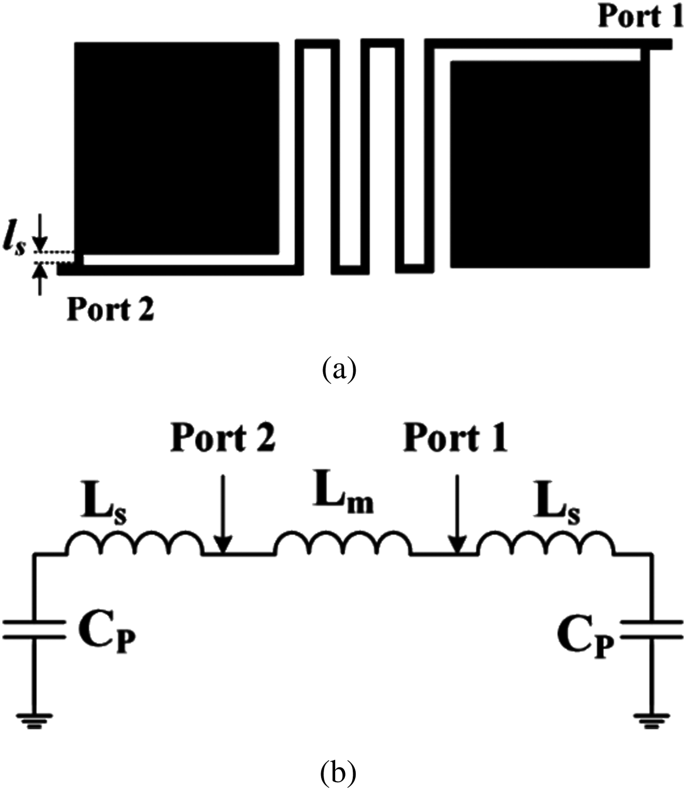
Fig. 1. Proposed basic structure (a) layout, (b) LC model.
In the LC circuit, the meandrous cell is replaced by the inductor L m, the small stubs with the physical length l s are modeled by the inductor L s, and the patch square capacitors are shown by C p. From the LC equivalent circuit, we can write the input impedance at the angular resonance frequency ω as follows:
 $$Z_{in} = \displaystyle{{[1 - \omega ^2L_sC_p] \times [1 - \omega ^2(L_s + L_m)C_p]} \over {\,j\omega C_p[2 - \omega ^2C_p(2L_s + L_m)]}}.$$
Since the proposed basic structure is symmetric, we can do the even and odd modes analysis. The odd and even modes resonance frequencies can be obtained for the input impedance Z in = 0 and Z in−1 = 0, respectively [Reference Hayati, Noori and Adinehvand14, Reference Rezaei and Noori15]. Accordingly, the even and odd modes angular resonance frequencies (ω e and ω o) are calculated as follow:
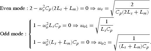 $$\eqalign{& {\rm Even}\;{\rm mode}:2 - \omega _e^2 C_p(2L_s + L_m) = 0 \Rightarrow \omega _e = \sqrt {\displaystyle{2 \over {C_p(2L_s + L_m)}}} \cr & {\rm Odd}\;{\rm mode}:\left\{ \matrix{1 - \omega _o^2 L_sC_p = 0 \Rightarrow \omega _{o1} = \sqrt {\displaystyle{1 \over {L_sC_p}}} \hfill \cr 1 - \omega _o^2 (L_s + L_m)C_p = 0 \Rightarrow \omega _{o2} = \sqrt {\displaystyle{1 \over {(L_s + L_m)C_p}}}. \hfill} \right.} $$
 Due to the small stub features, we can assume that L s ≪ L m. Therefore, 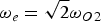 $\omega _e = \sqrt 2 \omega _{O2}$ while ω o1 > ω o2 and ω e. Hence, ω o1 is a harmonic created by the physical length l s [Reference Rezaei and Noori15]. Moving this harmonic to higher frequencies is desirable so that smaller L s results in shifting of this harmonic to the right. According to this, the length l s is decreased as far as possible. If we can tune ω o2 and ω e for 0.8 GHz GSM applications, then it can be said that with a good approximation ω e ≈ ω o2. For ω e = ω o2 = 2π × 0.8 × 109, C p × L m ≈ 1400. Therefore, the resonance frequency can be obtained by increasing the length of meandrous cell and incorporating it in a small space. According to above discussion, we can miniaturize the overall size, tune the resonance frequency and suppress the harmonics simultaneously. Since the proposed basic structure is a single-mode resonator, it can be upgraded to a bandpass filter by additional optimization. The layout configuration of the designed bandpass filter is depicted in Fig. 2, where all dimensions are in mm. It has a symmetric structure consisting of the meandrous cells connected to the patch structures. Figure 3(a) illustrates the frequency response of the proposed filter. It is depending on the dimensions of physical lengths L 1, L 2, and L 3. Therefore, the frequency responses as a function of L 1, L 2, and L 3 are shown in Fig. 3(b)–(d), respectively. Figure 3(b) demonstrates the increasing of L 1 which makes the channel wider. According to Fig. 3(b)–(d), increasing the mentioned lengths shifts the resonance frequency to the left. The frequency response of the proposed filter is optimized by tuning these physical lengths consisting of the lengths of patch, meandrous, and small cells.
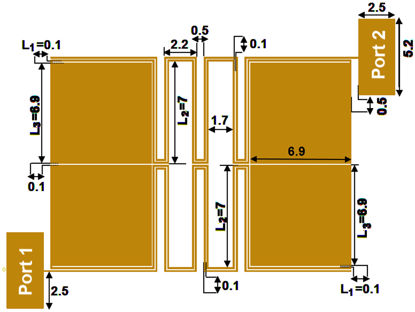
Fig. 2. Layout configuration of the proposed filter with its corresponding dimensions in mm.

Fig. 3. (a) Frequency response of the proposed filter, (b) S 21 as a function of L 1, (c) S 21 as a function of L 2, (d) S 21 as a function of L 3.
After designing of the proposed filter, two similar filters are integrated to have two channels. In order to avoid frequency interference, these filters are a little different in dimensions. By decreasing the difference in dimensions between the two filters, the created passbands will be closer to each other. This increases the losses and decreases the isolation between channels. Therefore, the additional optimizations are done to have a high performance and close channels. By integrating two bandpass filters, a microstrip diplexer is achieved as shown in Fig. 4 with its corresponding dimensions in mm. The dimensions of the bandpass filter connected to port 2 and common port 1 is same with Fig. 2. The proposed diplexer consists of meandrous cells connected to the engraved patch structures. The filters are integrated using a small simple transmission line connected to the common port. This structure can save the size and improve the isolation between channels simultaneously.

Fig. 4. Layout configuration of the proposed diplexer.
Results and discussion
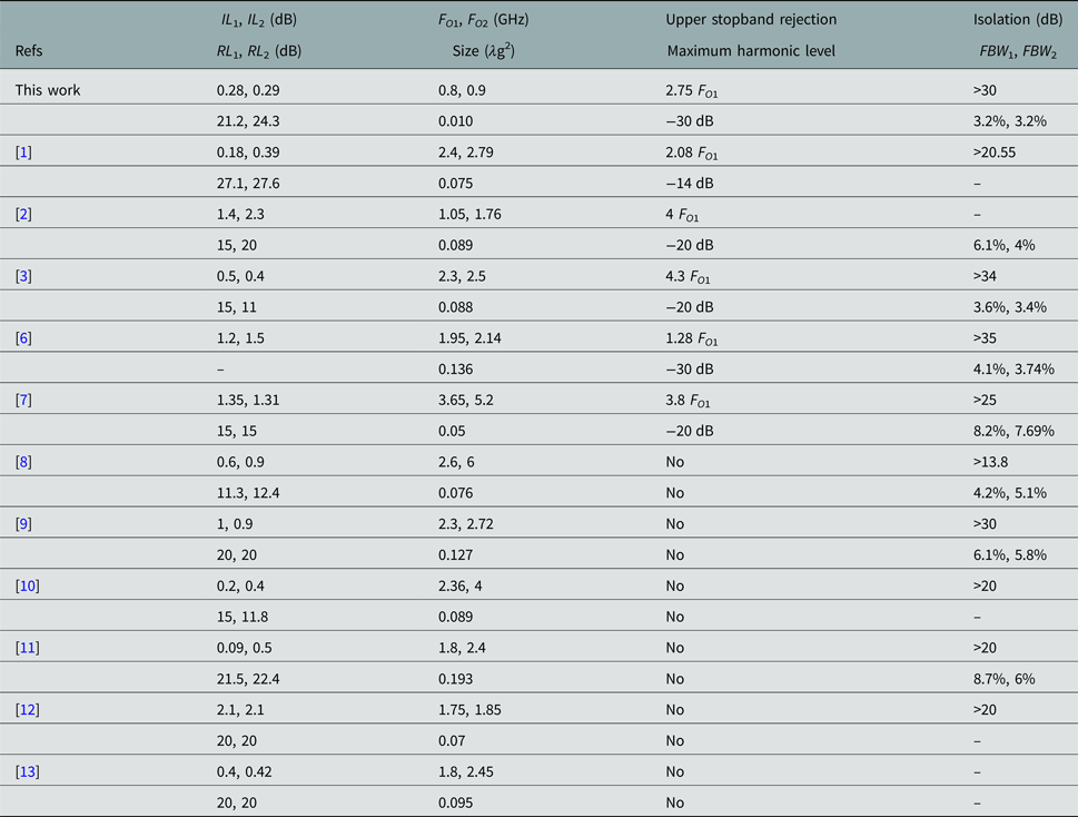
The proposed diplexer is simulated by Advanced Design System (ADS) full-wave EM simulator. It is fabricated on a Rogers_RT_Duroid5880 substrate with ε r = 2.22, h = 31 mil, and a loss tangent of 0.0009. An Agilent network analyzer N5230A carried out the measurements. Figure 5(a) depicts the simulated and measured S 21 and S 31. It shows that the introduced diplexer works at 0.8 and 0.9 GHz, which makes it appropriate for GSM applications. The first channel is from 0.786 to 0.811 GHz and the second channel is from 0.889 to 0.918 GHz with the FBWs of 3.12 and 3.2% for the first (FO 1) and second (FO 2) channels, respectively. The narrow channels make it suitable for the long-range communication applications. The designed diplexer has the low ILs of 0.28 and 0.29 dB at the first and second channels, respectively. Due to the copper and junction losses, the measured ILs are almost 0.4 dB more than the simulated results. As shown in Fig. 5(a) the first and second harmonics are suppressed with a maximum level of −30 dB. Figure 5(b) shows the simulated and measured common port RL and the isolation between the channels. The RLs at the lower and upper channels are better than 21.2 and 24.3 dB, respectively, while the isolation between channels is better than −30 dB. The proposed structure is well miniaturized with an overall size of 25 mm × 30.1 mm = 0.097 λg × 0.11 λg, where λg is the guided wavelength on the substrate at the first resonance frequency. A photograph of the fabricated diplexer is depicted in Fig. 5(c). The size and performance of proposed diplexer are compared with the previous works. The comparison results are listed in Table 1. According to the comparison table, the proposed diplexer has the minimum size. Meanwhile, it has relatively low losses and high isolation.

Fig. 5. (a) Simulated and measured S 21 and S 31, (b) isolation and common port return loss, (c) a photograph of the fabricated diplexer.
Table 1. Comparison between the proposed diplexer and previous works

Conclusion
In this paper, a compact microstrip diplexer is designed based on proposing a novel microstrip basic structure. The proposed diplexer consists of engraved meandrous cells and patch structures. In order to tune the resonance frequencies at 0.8 and 0.9 GHz, the meandrous cells are embedded in the least possible area. Meanwhile, the dimensions of patches and meandrous cells are selected so that the overall size of our diplexer is only 0.01 λg2 which is the minimum in comparison to the pervious works. The introduced diplexer not only has the low insertion and RLs at both the channels, but also we can see a relatively high isolation between its channels. Moreover, the first and second harmonics are suppressed with a maximum level of −30 dB.
 Abbas Rezaei is an Assistance Professor of Electrical Engineering in Kermanshah University of Technology. Abbas Rezaei received the BSe, MSe, and Ph.D. degrees in Electronics Engineering from Razi University, Kermanshah, Iran, in 2005, 2009, and 2013, respectively. His current research interests include computational intelligence and RF and microwave circuits.
 Leila Noori received B.S. and M.S. degrees in Electrical Engineering from Razi University in 2009 and 2011 and Ph.D. degree in Electrical Engineering from the Shiraz University of Technology in 2015. Main research interests are design and fabrication of microwave device such as microstrip filter, couplers, low noise amplifiers, diplexers, etc.