I. INTRODUCTION
The trend in modern radio communication systems has been moving toward carrier signals at millimeter wave (mm-wave) frequencies. Signals at such high frequencies can be generated through the frequency multiplication of a lower-frequency signal, or by optical heterodyning, where a signal at an arbitrary frequency can be generated by detecting the interference of two or more phase-locked optical laser modes, separated by the desired carrier frequency, by means of a photo-detector (PD). An electrical double sideband (DSB) spectrum is created at the PD if the laser pump current is varied with a modulation signal. Any instability present in the heterodyne carrier signal translates into an instability present in the desired output signal of the system, namely the information-carrying sidebands, which is why the transmission quality is strongly dependent on the purity of the carrier. It thus ultimately depends on how well the phases of the optical modes can be locked together.
We have previously demonstrated the impact of phase noise in an mm-wave communication system where the carrier signal is provided by heterodyning the optical modes of a free-running passively mode-locked laser diode (MLLD) [Reference Brendel, Poëtte, Cabon and Van Dijk1]. Such laser diodes are potentially low-cost devices, which are easy to integrate, but they exhibit rather high-frequency jitter and/or phase noise (−55 dBc/Hz at 10 kHz offset from the carrier, and a carrier variation of ≈600 kHz) [Reference Van Dijk, Enard, Buet, Lelarge and Duan2]. Furthermore, the precision of frequency adjustment in the manufacturing process is limited to a few hundred MHz to a few GHz. Unlike a voltage-controlled oscillator (VCO), the MLLD does not give access to a physical quantity, which can be used to fine-tune the oscillation – which hinders the construction of stabilization loops and is therefore problematic in the design of high data rate communication systems.
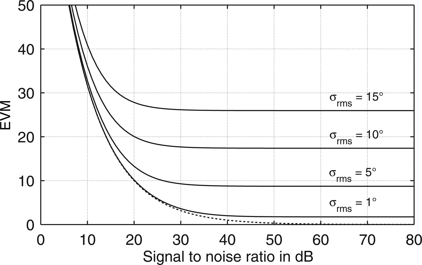
A communication system has to adhere to a well-defined spectral mask. Limited long-term stability in frequency, frequency jitter, or imprecise selection of the band center frequency can cause leakage into adjacent channels. At the receiver, requirements on the carrier recovery mechanisms must be tightened. Furthermore, increased phase noise will spoil the signal quality even at a stable center frequency. Error vector magnitude is a common figure of merit for transmission quality defined in most communication standards (see e.g. [3]). Georgiadis has investigated the relationship between the signal-to-noise ratio (SNR), the root-mean-square (rms) phase error σ rms and the Error vector magnitude (EVM) for the case where the peak symbol power equals the average symbol power [Reference Georgiadis4]:
 $$EVM_{rms}=\sqrt {{1 \over {SNR}}+2 - 2\cos\lpar \sigma _{rms} \rpar .}$$
As can be seen from Fig. 1, σ rms ≠ 0 introduces a constant error floor even for very high SNR values (the dashed line corresponds to σrms = 0). It is thus paramount for any communication system to minimize σrms by stabilizing the transmit (Tx) signal in both frequency and phase.

Fig. 1. Impact of phase noise on EVM. Dashed line: ideal case, no phase noise.
Typically, phase-locked loops (PLLs) are employed to stabilize the inherently unstable signal of a VCO [Reference Egan5]. The PLL principle relies on the fact that there exists a monotonous relationship between the physical quantity influencing the oscillation (e.g., the capacitance in an LC tank in a VCO) and an electrical signal controlling this physical quantity (e.g., the voltage). The PLL principle has been extended to include laser oscillators and opto-electronic components in optical PLLs [Reference Buckman, Georges, Park, Vassilovski, Kahn and Lau6]. If, however, the design of the oscillator does not allow access to such a physical quantity (as in the case of various laser-based techniques, where the oscillation cannot be fine-tuned by varying the laser pump current), the construction of a conventional PLL is not feasible. Other techniques commonly employed in the context of laser physics like optical active mode-locking [Reference Avrutin, Marsh and Portnoi7] or optical feedback loops [Reference Van Dijk, Enard, Buet, Lelarge and Duan2, Reference Merghem8] tend to be complex and allow at most a stabilization of frequency – but no tuning capability.
In this work, we present a full analysis of a novel stabilization and tuning architecture allowing the stable transmission of a sideband signal in the presence of long-term carrier instability (jitter or drift) and increased phase noise; its key principlewas presented in [Reference Brendel, Zwick, Poëtte and Cabon9]. Here, we show a complete system demonstrator encompassing full heterodyne up-conversion, and we enclose a thorough Laplace analysis of the resulting noise suppression. The paper is organized as follows: In Section II, the stabilization technique is introduced. We discuss the capture ranges of the proposed architecture in Section III. The loop response to phase noise is evaluated in terms of the phase power spectral density(psd). Simulations and measurements on the test hardware according to Section IV are compared in Section V. The results are discussed in Section VI, and we will conclude the work in Section VII.
II. STABILIZATION PRINCIPLE
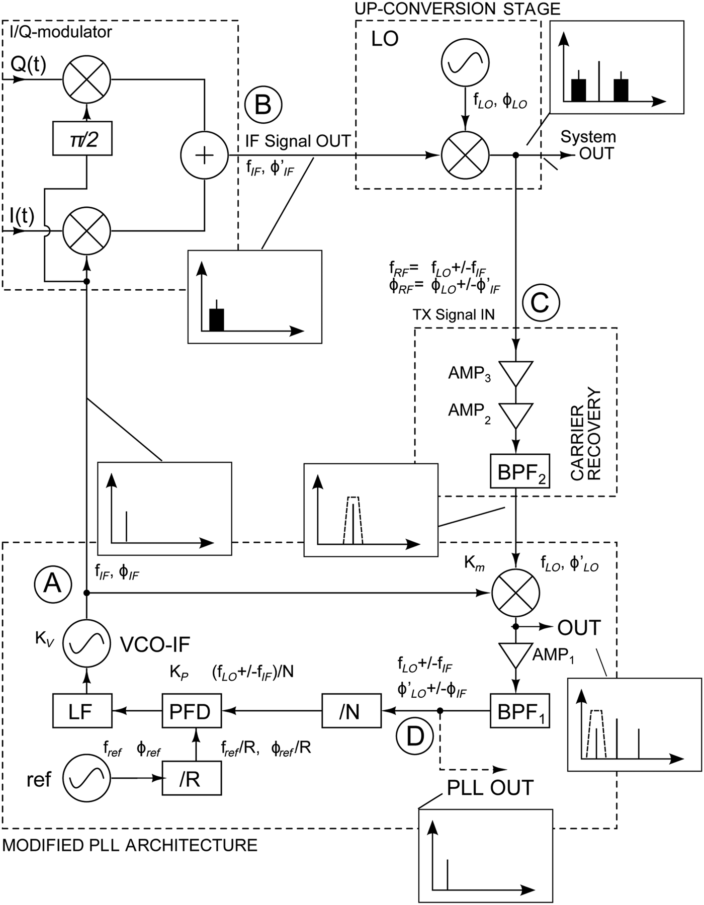
The proposed architecture is depicted in Fig. 2. The bold letters A–D are intended for an easy comparison between the block diagram and the hardware implementation shown in Fig. 3. For a discussion of the inclusion of an optical sub-system, see [Reference Brendel, Zwick, Poëtte and Cabon9]. The key ideas are the following:
– The complete stabilization structure incorporates a PLL modified by a loop mixer and a band-pass filter, as well as an up-conversion stage where the DSB spectrum is created and a carrier-recovery stage on the Tx's side.
– The modified PLL acts on the mixing product of the carrier signal provided by the up-conversion stage (mixing of LO and IF oscillators).
– This mixing product, i.e. the upper (USB) or lower (LSB) sideband in the DSB spectrum, is the desired output signal of the system. The mixing product carries the contributions from both the Local Oscillator (LO) in the up conversion stage of Fig. 2 and Intermediate Frequency (IF) delivered by the VCO in the PLL of Fig. 2; regarding the phase noise present in the mixing signal, it is correlated to both sources. The PLL can thus be constructed either to act on the LO – Which, as we have stated before might not be possible in the case of optical LO generation – or on the IF oscillator.
– The mixing product in the DSB spectrum exhibits a bandwidth. However, inside the loop, the phases of a single-tone mixing product and a stable reference must be compared. It is thus necessary to suppress the band around the center frequency f RF = f LO ± f IF. This is done by band-pass filtering (BPF2) the carrier from the DSB spectrum in the carrier recovery stage. The recovered LO is then mixed again with the unmodulated IF signal. A band-pass filter BPF1 then selects the USB or LSB.
A conventional PLL can be described in Laplace notation by the forward (open-loop) and reverse transfer functions of the loop for the reference phase φ ref as input signal:
 $$G_F \lpar s\rpar =K_P \cdot Z_{LPF} \lpar s\rpar \cdot {K_V \over s}\comma \;$$
 $$G_R \lpar s\rpar ={1 \over N}\comma \;$$
where K P is the phase-detector gain, Z LPF is the loop filter transfer function, K V is the sensitivity of the VCO, and N is the frequency divider value [Reference Egan5]. Here, these functions must be modified to include additional components: the loop mixer and the band-pass filter BPF1, as well as an amplifier AMP1 necessary in order to provide sufficient RF power to the PLL.
1) Effect of a mixer Regarding the phase or the frequency of a signal, the mixing process is a linear translation. Through mixing process, the sidebands are formed at the sum and the difference of the input frequencies. Assuming up-conversion in an ideal mixer:
(3a) $$\phi _{RF\comma USB}=\phi _{LO}+\phi _{IF}\comma \;$$(3b)for the USB and the LSB, respectively. In the PLL, most computations involve changes from steady state and are evaluated at an offset from center frequency. The center frequency itself (shifted by mixing) is not relevant [Reference Egan5]. If the PLL acts on a mixing product, the phase-frequency detector must compare the sideband phase to the reference phase. This approach is justified as long as it does not put loop stability at risk, i.e. as long as we design the loop for sufficient phase margin. In the following, the LSB is selected in order to keep the operating frequency of the PLL as small as possible. The mixer's conversion loss (negative gain) can be represented in the respective transfer function by a factor K m.$$\phi _{RF\comma LSB} =\phi _{LO} - \phi _{IF}\comma \;$$
2) Low-pass equivalent for band-pass filtering: The effect of the band-pass filter on the loop transfer functions will affect the loop response to phase noise. It is in general possible to find a low-pass equivalent representation for a band-pass filter in a PLL as long as the modulation deviation is small [Reference Egan5]. In our case, the situation is even simpler as we already design the band-pass filter starting out from a low-pass prototype. The low-pass prototype is designed to follow an attenuation characteristic of G 2eqLPF(f). In terms of the filter transfer function Z eqLPF, G 2eqLF(f) = |Z eqLPF(jf)|2.
3) Effect of RF amplifiers: An amplifier in the loop can, in a first approximation, be represented by a gain factor K a. In a phase-locked loop optimized for CW operation, the amplifiers operate at a fixed frequency, which is why the gain can be thought of as constant.
4) Modified transfer function: The signal is tapped after the mixer (“OUT”). All components thereafter are considered part of the reverse transfer function. The mixer becomes a part of the forward transfer function.


 $$G_F^{\prime} \lpar s\rpar =\lpar \!-\! 1\rpar \cdot G_{F} \lpar s\rpar \cdot L_{WD} \cdot \lpar\! -\! 1\rpar \cdot K_{m}\comma \;$$
 $$G_R^{\prime} \lpar s\rpar =K_{a1} \cdot Z_{eqLPF} \lpar s\rpar \cdot G_R \lpar s\rpar .$$
The factor L WD reflects the fact that only half of the VCO power is routed back to the loop; a Wilkinson divider with a nominal split of L WD = 0.5 is employed at the branching point. The factor (−1) represents the phase reversal in the LSB, which is compensated for by reversing the polarity of the charge pump with a gain of K P (again, factor −1).
Fig. 2. Transmitter architecture: stabilization principle. Letter A–D correspond to points A–D in Fig. 3.
Fig. 3. Photo of PLL Demonstrator. Not shown in the picture: up-conversion stage (Anritsu 6877B and mixer at input C). Compare points A–D to letters A–D in Fig. 2.
We then define the closed-loop transfer functions where we refer to H LP (s) as the low-pass transfer function, and to H HP (s) as the high-pass transfer function:
 $$H_{LP} \lpar s\rpar ={G_F^{\prime} \lpar s\rpar \over {1+G_F^{\prime} \lpar s\rpar G_R^{\prime} \lpar s\rpar }}\comma \;$$
 $$H_{HP} \lpar s\rpar ={1 \over {1+G_F^{\prime} \lpar s\rpar G_R^{\prime} \lpar s\rpar }}.$$
Note that the proposed principle is not identical to conventional sliding IF phase-locked loops, where a stable translation oscillator is used to shift the (usually down-converted) signal within a variable IF range. Such a system does not accept increased phase noise or jitter on the LO because it is not the mixing product, which is fedback within the loop structure. The principle shown here can be used for any type of noisy LO generation, in particular for those optically generated in the millimeter wave range, where few means of stabilization are available.
III. CAPTURE AND HOLD-IN RANGES
The PLL is supposed to lock the modulation sideband generated at the loop mixer from the output signal of the IF oscillator and the recovered LO signal. The capture range refers to the range of frequencies for which the unlocked PLL can become locked to the reference after a certain capture time, which will we denote T cap. Once locked, it is required to counter-act the phase and frequency deviations of the modulation sideband. The range of frequencies for which the PLL can track the variations of the controlled signal is referred to as hold-in range.
The perturbations we deal with are the phase and frequency deviations of the modulation sideband. These deviations depend on both the IF oscillator and the LO used in the up-conversion stage. We consider the following cases:
– Case 1, phase noise: The LO center frequency is stable. The variation of the modulation sideband frequency is mostly influenced by the IF oscillator. Through mixing, the phase of the modulation sideband experiences a sudden shift.
– Case 2, frequency jitter: The LO center frequency is not stable. A slow variation of the sideband frequency will occur which is due to the variations of both the IF and the LO oscillator frequency. At the loop mixer, both frequency and phase of the modulation sideband experience a sudden change.
For the following, we assume that the PLL comprises a charge-pump phase-frequency detector (PFD). In locked state, a PLL featuring a charge-pump PFD does not have a residual frequency error, nor a steady-state phase error [Reference Best10].
Capture range: Whether or not the PLL will lock is determined by two aspects. The first is sufficient phase margin. While a very large phase shift might be produced at the mixer, it primarily concerns the center frequency of the signal to be controlled (here: f LO–f IF). It is important to note that this phase shift at the absolute center frequency does not enter into the loop model. The phase margin is calculated at the unity gain offset modulation frequency from the center frequency of the controlled signal. The notion of phase margin is essentially independent from the absolute frequency or phase of the controlled signal and can be considered separately in loop design. The second aspect is the actual capture range of the PLL. If a PFD is used, the average output signal of the PLL varies monotonically with the frequency error. Theoretically, the capture range is infinite [Reference Best10]. In practice, it is limited by the frequency range of the controlled (IF) oscillator. As a consequence, the PLL will always lock – if the phase margin condition is met – and the frequency error will settle to zero. Likewise, the range of possible phase error allowed for stable operationis the full 360° range for a PFD [Reference Best10]. The residual phase will also settle to zero. In Case 1, we can therefore be sure that the PLL will lock.
In Case 2, the change in LO frequency must be slow compared to the time span necessary for capture, assuring that the PLL can actually follow the frequency variation of the sideband, as T cap is not infinitesimally short. It depends on several parameters [Reference Best10],
 $$T_{cap}=2 \cdot \Delta f_0 \cdot {NC_1 \over K_P K_V }\comma \; $$
where Δ f 0 represents the difference between the reference frequency and the scaled-down initial frequency of the controlled signal (here, the modulation sideband), and C 1 is the loop filter capacitance that loads the PFD. In equation (10), we have neglected the gains of the loop amplifier, the band-pass filter, and the loop mixer. All values considered, T cap can be estimated in the range of hundreds of ns to 1μs.
Hold-in range: The hold-in range is obtained by calculating the frequency where the phase error is at its maximum. In Case 1, the use of a charge-pump PFD results in a hold-in range which is theoretically infinite [Reference Best10] as any phase error can be corrected by the PLL. As for the real capture range, the real hold-in range is limited by the operating range of the controlled oscillator.
In Case 2, the charge-pump PFD will correct the frequency error of the locked PLL. As the LO frequency changes over time, two conditions must however be fulfilled in order to exploit the hold-in range of the PLL. First, the LO frequency must not reach a value that would result in a difference frequency outside the IF oscillator's frequency range. Second, the control mechanism of the PLL must be fast enough to follow the frequency variations. The decisive factor is the loop bandwidth. It can easily be designed to cover several hundreds of kHz to several MHz.
We thus expect the PLL to lock and stay locked if T cap is small compared to the rate of the frequency variation of the LO (≈ms), and as long it does not exceed the frequency range of the IF oscillator.
IV. PLL DEMONSTRATOR
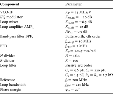
A modular demonstrator was implemented for a first demonstration of the concept. We emphasize that the choice of components was linked to their off-shelf availability but leaves room for optimization which we will consider in the parametric analysis in the following Section V. The demonstrator is shown in Fig. 3. The carrier signal is provided by a commercial signal generator (Anritsu 68377B). The DSB spectrum is created in a mixer identical to the mixer in the loop (not shown in the figure for limited space) and fed into the demonstrator at “Tx Signal IN” (input C). Table 1 gives a summary of the relevant parameters.
Table 1. Parameters
The main component of the PLL is a chip (ADF4108) comprising a low-noise digital PFD, a charge pump, and programmable dividers for both the RF input signal (value N) and the reference signal (value R). The reference signal is delivered by a signal generator, allowing the use of different reference frequencies, and selectable comparison frequencies f PFD for the PFD. The surface-mount VCO-IF delivers signals at frequencies from 1.77 to 1.83 GHz at an output power of 3 dBm. Its phase noise for offset frequencies >1 MHz is 161 dBc/Hz. With a charge pump voltage of 5 V, and a target control voltage of the VCO-IF of about 2 V, the loop filter could be realized as a passive RC network and was designed for third order and a loop bandwidth of f BW = 210 kHz at a phase margin of φm = 27°. The surface-mount I/Q-modulator is a vector modulator operating in the range from 1.5 to 2.5 GHz with a maximum output power of 7.1 dBm and an output noise floor of −158 dBm/Hz (its output is “IF signal OUT”). The mixer in the loop is a surface-mount double-balanced MMIC mixer operating in the range from 1.8 to 5 GHz. A DSB spectrum is created with principal spectral components at 3.2 GHz(LSB), 5 GHz (carrier), and 6.8 GHz (USB); the LO-to-RF suppression of about 30 dB is enough for both the carrier recovery path (where we actually need the LO component in the spectrum) and in-loop up-conversion (where it can be filtered). BPF1 is designed in the low-pass domain with a maximally flat Butterworth response of the following characteristics: passband edge f cut-off = 50 MHz, stopband edge 100 MHz, passband attenuation L ar = 0.5 dB at f cut-off, stopband attenuation L A at the stopband edge −40 dB. The measured filter loss at the band-pass center frequency f BPF = 3.2 GHz is −3.4 dB, and the measured phase shift is θBPF1 = 0.65°. Its influence on phase margin is negligible in the direct vicinity of the center frequency.
The carrier recovery stage consists of two amplifiers with gains K a2,dB = 22 dB (OP1dB = 8 dBm, NF = 1.86 dB) and K a3,dB = 8 dB (OP1dB 17.5 dBm, NF = 8 dB), as well as the band-pass filter BPF2 designed as a coupled line band-pass filter centered at 5 GHz.
It is sufficient to consider the insertion loss of the band-pass filter BPF2 (K BPF2,dB = −5 dB) and its phase shift θBPF2 = 21° introduced at 5 GHz instead of its transfer function. We can do so because its bandwidth of approximately 200 MHz is large compared to the loop bandwidth. The carrier recovery stage is designed to provide a drive power of ≈10 dBm at the LO port of the loop mixer.
V. LOOP RESPONSE TO NOISE
A. Phase power spectral density simulations
Phase noise can be understood as the modulation of the carrier frequency by a random noise waveform. It is common practice to treat this phase modulation as a zero-mean stationary random process quantified by its two-sided psd function S φ(f). Its rms phase error σrms is obtained through integration,
 $$\sigma _{rms} = \sqrt {\vint_{ - \infty }^{+\infty } S_\phi \lpar f\rpar df} .$$
After demodulation, S φ(f) includes both negative and positive frequencies. In phase noise measurements, it is common to consider only the positive frequencies and hence, the single sideband (SSB) psd L φ(f). The usual way to determine the loop's total response is to determine an appropriate closed-loop transfer function H i(s) from a source i to the output. Starting from the component's psd S φ,in,i(f), the resulting psd at the output S φ,out,i(f) can be determined according to
 $$S_{\varphi \comma out\comma i} \lpar f\rpar = S_{\varphi \comma in\comma i} \lpar f\rpar \cdot \vert H_i \lpar jf\rpar \vert^2 $$
where the Laplace variable of equation (8) is s–2πf. The noise waveform is a voltage or a current, so the squared closed-loop transfer function appears in the output psd which can then be obtained by summing up the various noisecontributions of oscillators, mixer, amplifiers, and filters,
 $$S_{\phi\comma TOT} \lpar f\rpar = \sum\limits_i S_{\phi\comma out\comma i} \lpar f\rpar . $$
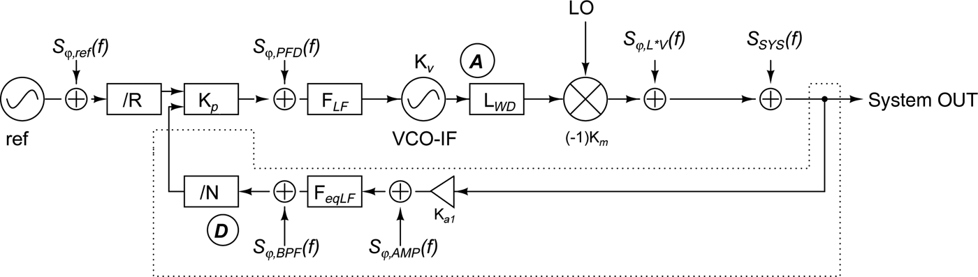
This procedure is reflected in the component noise equivalent circuit as depicted in Fig. 4. Each component is assumed ideal and the noise contribution is inserted as a noise source with the respective phase noise psd S φ,in,i. The noise contribution of the loop filter and the phase noise originating in the N- and R-dividers have been neglected. It is then necessary to determine the influence of the different components.
Fig. 4. Circuit equivalent for phase noise analysis, corresponds to dashed box “modified PLL architecture” in fig. 2.
Reference phase noise (described by Leeson's model [Reference Leeson11]) will be scaled down by the reference divider value, and transformed by the low-pass transfer function to the output of the loop:
 $$S_{\varphi \comma out\comma ref} \lpar f\rpar = S_{\varphi \comma ref} \lpar f\rpar \cdot \displaystyle{1 \over {R^2 }}\vert H_{LP} \lpar jf\rpar \vert^2. $$
It is preferable to pick a high reference frequency f r if the reference phase noise can be scaled down by a high value of R.
The chip phase noise will be scaled by the charge pump gain and transformed to the output of the loop, again by the low-pass transfer function:
 $$S_{\varphi \comma out\comma PFD} \lpar f\rpar = S_{\varphi \comma PFD} \lpar f\rpar \cdot \left\vert \displaystyle{1 \over {K_p }}\right\vert ^2 \vert H_{LP} \lpar jf\rpar \vert ^2. $$
Both amplifier noise and the contribution of the noise figure of the band-pass filter can be modelled as flat. Their noises will be transformed by the loop according to
 $$S_{\varphi\comma out\comma y} \lpar f\rpar = S_{\varphi\comma y} \lpar f\rpar \cdot N^2 \cdot {\vert {H_{LP} \lpar jf\rpar }\vert}^2. $$
The VCO signal passes through the power divider and suffers a conversion loss by the loop mixer,
 $$S_{\varphi\comma VCO}^{\prime} \lpar f\rpar = {\vert {L_{WD} } \vert}^2 \cdot {\vert {\lpar\! -\! 1\rpar \cdot K_m } \vert}^2 \cdot S_{\varphi\comma VCO} \lpar f\rpar . $$
Both S φ,VCO(f) and S φ,LO(f) are described by Leeson's model [Reference Leeson11].
In the carrier recovery stage, the LO signal is amplified, filtered and attenuated by the mixer's LO-to-RF isolation:
 $$\eqalign{S_{\varphi\comma LO}^{\prime} \lpar f\rpar & = {\vert {K_{a3}} \vert}^2 \cdot {\vert {K_{a2} } \vert}^2 \cdot {\vert {K_{BPF2} } \vert}^2 \cdot {\vert {exp\lpar j\theta _{BPF2} \rpar } \vert}^2 \cr & \quad \cdot {\vert {K_{LO - RF} } \vert}^2 \cdot S_{\varphi\comma LO} \lpar f\rpar .} $$
From equation (14), we see that by carefully selecting the amplifiers and the filter, it is possible to design the carrier recovery stage such that it is quasi-transparent with respect to LO phase noise. The loop mixer and the mixer in the up-conversion stage can therefore be operated under similar conditions. When the recovered LO signal and the VCO-IF signal pass through the mixer, the phase psd's at the mixer's RF output will be convoluted to give:
 $$S_{\varphi\comma L \ast V} = S_{\varphi\comma LO}^{\prime} \lpar f\rpar \ast S_{\varphi\comma VCO}^{\prime} \lpar f\rpar . $$
Through the loop, this combined phase noise will be transformed by the high-pass transfer function,
 $$S_{\varphi\comma out\comma L \ast V} = S_{\varphi\comma L \ast V} \cdot {\vert {H_{HP} \lpar jf\rpar } \vert}^2 . $$
For the electrical measurements, the noise figure of the recovered LO is determined by the signal generator's noise floor. This noise will be transformed through the loop in the high-pass transfer function:
 $$S_{\varphi\comma out\comma SYS} \lpar f\rpar = S_{\varphi\comma SYS} \lpar f\rpar \cdot {\vert {H_{HP} \lpar jf\rpar } \vert}^2 . $$
When we add the results of equations (10) – (17) in equation (9), we obtain the over-all response of the loop to phase noise. In simulation, we can now vary the different parameters in order to state more precisely the requirements on the PLL. It is assumed that the phase noise of the LO is a given parameter which cannot be altered by the system designer. At a given noise level, the optimum loop bandwidth is found at the intersection of the f −2 slope and the noise floor. The loop bandwidth sets the minimum phase-frequency detector frequency for stable operation (usually a factor of 10 must be maintained [Reference Egan5]). The simulation results are shown in Fig. 5: In Fig. 5(a), we observe how in-loop phase noise scales with the divider value N (values: 50, 100, 200, 400, 800 and 1600). Inband phase noise can be suppressed by selecting the smallest possible divider ratio N, i.e. the highest possible f PFD. Figure 5(b) shows a variation of the charge pump gain (for K P = 0.32, 0.48, 0.79, 1.24, and 1.59 mA/rad). We conclude that the charge pump gain should be chosen for sufficient damping of the transfer function at the loop bandwidth. A high-Q reference oscillator whose nominal frequency is as high as possible is crucial for in-loop phase noise suppression. The reference phase noise is then scaled down by the R-divider. For high VCO input capacitances and high f PFD, the loop filter can be implemented as an active filter that will not load the charge pump capacitively.
Fig. 5. Simulations. Dashed curve corresponds to the sideband phase psd when PLL is inactive. Bold black curve corresponds to the simulated curve for the PLL demonstrator as prepared. (a) N variation, (b) Kp variation, (c) NF variation, (d) Comparison: PLL as realized and possible improvements.
While the lower limit of integration in equation (7) does not have a severe impact on the accumulated phase error, the upper limit does matter. At large offsets, the amount of additional phase noise that has to be accounted for when pushing the upper integration limit higher, is highly dependent on system noise. Figure 5(c) shows the influence of the system noise figure F total (steps of 5 dB up to 55 dB).
Adhering to those design rules which can be extracted from this parametric analysis, the PLL can be improved under the assumption that the LO phase noise and the VCO-IF phase noise stay the same. With the same chip, the PFD frequency can be increased to mbox f PFD = 50 MHz, allowing a minimum divider value of N = 64 for stabilization at 3.2 GHz. The charge pump gain is set to I P = 0.79 mA/rad. A third-order active loop filter in the so-called “standard feedback” topology was simulated (Nomenclatura as in [Reference Banerjee12]: C 1 = 0.63 pF, R 1 = 6.55 kΩ, C 2 = 19.7 pF, R 3 = 38 Ω, C 3 = 134 pF). The possible improvement of the total phase psd can be observed in Fig. 5(d), where the integrated phase error can be reduced from 1.52° to about 0.21°.
B. Measurements of the single sideband phase psd and EVM
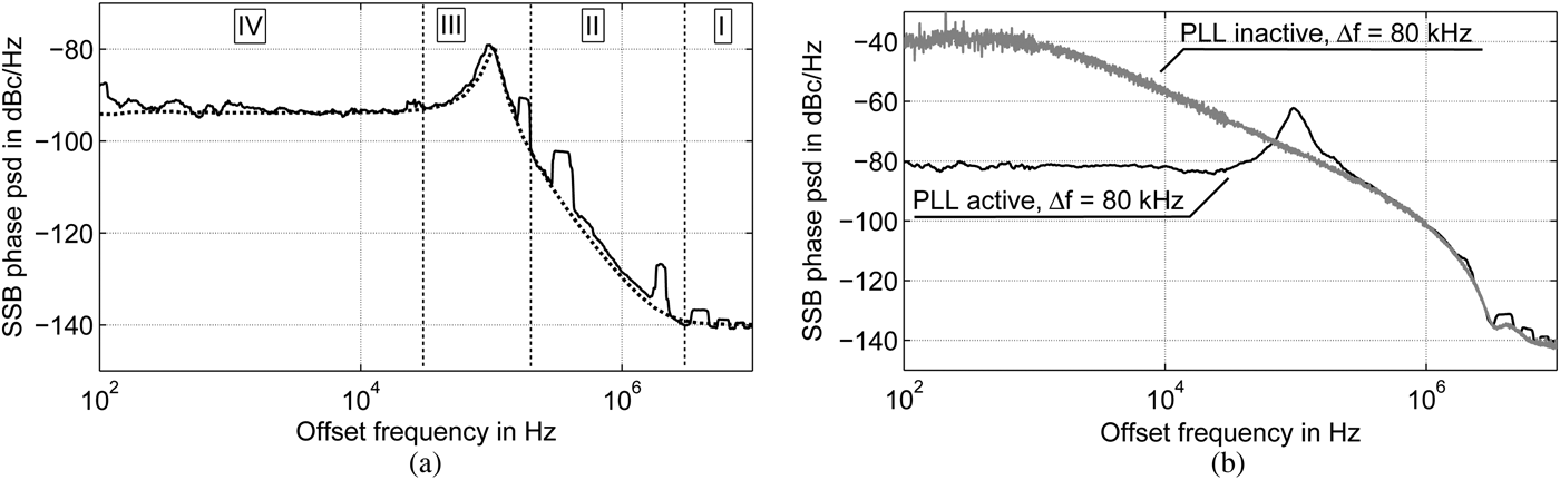
The phase noise performance of the loop itself is evaluated using an electrical LO. Here, it is supplied by a signal generator (Anritsu 68377B) at a frequency of 5 GHz. Different levels of LO phase noise can be tested using Gaussian noise (GN) frequency modulation (FM). This function of the generator requires the specification of a maximum FM deviation Δf. The FM rate is set such that the modulating frequency f m follows a Gaussian distribution between 0 Hz and 1 MHz, so that the modulation index β = Δf/f m is also Gaussian distributed. The modulation appears as phase noise on the generator's CW output signal while the center frequency is fixed. This way, the phase noise characteristics of the LO can be controlled. Figure 6(a) shows a comparison between the simulated curves and the measured results of the PLL without additional phase noise (Δf = 0 Hz), which coincide well and thus validate our loop noise model. We distinguish four differentregions of interest: at large offsets (1), the noise floor is largely determined by the chip noise scaled by the divider ratio N; up to the loop cut-off frequency (210 kHz approx.), the curve is largely determined by the oscillator noise resulting from the mixing of the LO and IF oscillators when free-running (2); the overshoot can be attributed to the loop filter function (3); and the plateau within the loop bandwidth is, to a large extent, scaled reference noise (4). The instability measured in the laser-based system used for comparison corresponds to a a phase noise that can be emulated choosing Δf + 80 kHz. Figure 6(b) shows two SSB phase psd curves measured on the LSB for the active and the inactive PLL. In the immediate proximity of the center frequency, the PLL suppresses the phase noise by as much as 40 dB. At an offset of 10 kHz, a suppression of 20 dB is achieved. Locally, the overshoot in the loop filter function causesthe phase noise level to rise, which is definitely an issue that needs improvement in a rigorous PLL redesign. In Fig. 7, the results of a data transmission experiment are shown. Here, the PLL was active (phase noise resulting from Δf = 80 kHz) and the I/Q ports of the demonstrator were fed by a digital baseband signal at 18 Mbps at a quadrature-phase-shift-keying (QPSK) format according to IEEE 802.11a [13]. The measured SNR for the modulated signal with the active PLL was about 26.5 dB. With an integrated rms phase error of 1.52°, this results in an EVM value of 6% according to equation (1) which was confirmed by measurement (see grey circle). As can be observed from Fig. 7, the floor value for higher SNR values is at about 3%. We conclude that the EVM is still limited by the SNR. With the PLL inactive and still under the condition of emulated phase noise at Δf + 80 kHz, the EVM was not reliably measurable but ranged of the order of 40% (for this reason, not shown in Fig. 7).
Fig. 6. Measurements with and without GN modulation, PLL active and inactive. (a) Comparison of simulated (dashed line) and measured (solid line) phase power spectral densities. No additional phase noise. (b) Measurements, PLL active and inactive. GN modulation with Df = 80 kHz. Phase noise suppression of 40 dB in the proximity of the center frequency.
Fig. 7. EVM analysis
VI. DISCUSSION
In the same figure, we have plotted the curve for σrms = 0.21° which results in EVM values close to the theoretical maximum (σrms = 0°), <1%, when design improvements are made according to Section V-A. At such small EVM values, other imperfections such as the I/Q imbalances of modulator and demodulator will most likely limit the transmission. Further improvement can thus only be expected if the SNR of the system can be improved.
So far, we have neglected the possible occurrence of time delays in the loop. In the event where a time delay T d is included at some point in the architecture, we might run into problems regarding loop stability. If T d occurs pe within the loop, the phase shift does not depend on the phase difference of the IF and the LO signal, mixed at the loop mixer. Instead, phase shifts proportional to the respective noise modulation frequency will be produced by T d. It is thus wide loop bandwidth which worsens the situation. In general, it is assumed that a delay is not critical as long as it is much smaller than the reciprocal of the loop bandwidth, which is in our case, 4.76 μs [Reference Egan5]. An SMA connector implies a time delay of about 50 ps, while a transmission line exhibits a time delay of 5 ps/mm. Adding up cables and connectors present in the measurement of the demonstrator, the overall delay ranges at most in the ns range and will be negligible compare to 1/f BW. Further reductions in the lengths of the signal paths can be envisioned by integrating the components on one board (as opposed to this modular approach).
VII. CONCLUSION
In a communication system in which an information signal is frequency-converted by mixing it with a high-frequency carrier, it is this up-converted signal we wish to stabilize or tune. If the signal modulation results in a DSB spectrum, the stability of the carrier is secondary as long as at least one of the sidebands is stable. Based on this consideration, a PLL can be modified to operate on a sideband signal. Its most striking feature is that it can provide a stable modulation band in the presence of high-carrier instability as manifested in frequency jitter and phase noise. This is valid for any type of LO generation, including optical techniques resulting in LO frequencies in the mm-wave range. We have shown a first proof of concept based on the system demonstrator presented in this paper. Electrical measurements have shown the feasibility of the loop, and the measurement results could be reproduced in the simulation. By simulation, the requirements on the loop's performance could be refined. If the design rules presented in Section V-A are respected, the resulting rms phase error can be decreased from 1.52° to 0.21°. The loop's IF synthesizer capability makes it possible to fully compensate for the drift of the LO frequency and to tune the sideband frequency to a nominal center value as required by the standard spectral masks. The phase noise could be suppressed within the loop's bandwidth by 40 dB.
Friederike Brendel received the Dipl. Ing. (M.S.E.E.) degree in Electrical Engineering and Information Technology from the University of Karlsruhe (TH), Germany in 2009. From October 2009 to October 2011, she was with the theInstitute for Microelectronics, Electromagnetism and Photonics (IMEP-LAHC) in Grenoble, France. From October 2011 to March 2013, she was with Institut für Hochfrequenztechnik und Elektronik (IHE) at the Karlsruhe Institute of Technology, Germany, where she received her PhD degree in early 2013. Her main research interests are optical RF generation and radio-over-fiber systems, in particular in the 60 GHz region.
Thomas Zwick (S′95-M′00-SM′06) received the Dipl.-Ing. (M.S.E.E.) and the Dr.-Ing. (Ph.D.E.E.) degrees from the Universität Karlsruhe (TH), Germany in 1994 and 1999. From 1994 to 2001 he was research assistant at the Institut für Hochfrequenztechnik und Elektronik (IHE) at the Universität Karlsruhe (TH), Germany. From 2001 to 2004, he was with the IBM T. J. Watson Research Center in Yorktown Heights, NY, USA. Since 2007, he is professor and director of the IHE at the KarlsruheInstitute of Technology, Germany. His research topics include wave propagation, microwave techniques, mm-wave antenna and system design, wireless communication and radar system design. Since 2008 he is president of the Institute for Microwaves and Antennas (IMA). T. Zwick became selected as a distinguished microwave lecturer for 2013 – 2015. He is author or co-author of over 200 technical papers and over 20 patents.
Julien Poëtte is an associate professor at Grenoble Institute of Technology, France. He received in 2002 an engineer diploma form the French Engineering School ENSSAT (National School for Applied Science and Technologies) with a specialization in optro-electronics. He obtained his Ph.D. in physics in 2005 from RENNES 1 University, France for his work in noise in laser dedicated to telecommunication. In 2008, he joined the IMEP-LAHC laboratory and his research activity is now on next generation of communication Systems involving microwave-photonics techniques at 60 GHz.
Béatrice Cabon (S′93-M′95) is a professor at Grenoble Institute of Technology (Grenoble-INP), France since 1989. She received the Ph.D. degree in microelectronics from Grenoble-INP in 1986. Since 1993, she is head of a research group on Microwave-Photonics techniques at the IMEP-LAHC laboratory in Grenoble (Institute for Microelectronics, Electromagnetism, and Photonics). She was coordinator of the IST-2001-32786 NEFERTITI with 28 organizations over nine countries, funded by the European Commission, and of the network of excellence FF6-IST-26592 ISIS with 19 organizations of 12 countries. Her research interests include microwave-photonics, photonic-microwave signal processing, and optical links for high bit rate signals. She has contributed to over 260 technical publications and is the editor of four books in these areas.