


I. INTRODUCTION
In recent years, there is an increasing interest in the use of terahertz (THz) technology for a number of applications such as sensing, communications, and biomedical applications [Reference Tonouchi1]. Due to this rapid development, demand for compact, fast, and reliable THz components such as tunable oscillators, mixers, and multipliers used in THz sources has increased. GaAs-based Schottky diodes are the most popular devices for building THz sources [Reference Maiwald2–Reference Guo, Xu and Qian7] and detectors [Reference Maestrini8–Reference Sobis, Wadefalk, Emrich and Stake11], mainly due to the high electron mobility, simplicity of integration with planar THz device structures, and fast operation. However, the performance of such planar GaAs Schottky diodes degrades at higher frequencies as a result of parasitic capacitances [Reference Mehdi and Siegel12], series resistances [Reference Tang and Stake13], and carrier velocity saturation effects [Reference Grajal, Krozer, González, Maldonado and Gismero14]. Researchers have minimized the parasitic capacitance by replacing GaAs substrate with a low dielectric substrate [Reference Crowe, William, Bishop, Meiburg and Mattlauch15] through wafer bonding and epitaxial lift off or selective vertical layer etch/release techniques. Such techniques add significant fabrication complexities to the overall device fabrication process [Reference Yoon16]. In addition, it should be noted that partial reduction of shunt capacitances is achieved by tuning design parameters such as decreasing substrate thickness to reduce the effective permittivity around the device and increasing pad-to-pad separation. It should also be noted that in standard applications, the thin substrate is attached to the surface of either a Si hemispherical lens or a quartz substrate allowing the use of membrane-supported diode structures. The series resistance can be reduced as well by choosing low-loss metals like silver, adjusting buffer layer thickness, and increasing doping level. However, the effect of buffer layer thickness in reduction of R s is not significant [Reference Tang17] and increasing the doping levels deteriorates other device characteristics like breakdown voltage and ideality factor [Reference Hudait and Krupanidhi18]. By taking these factors into consideration, there is an apparent need for an accurate modeling of THz planar Schottky diodes in order to improve the device structure for enhanced Schottky diode-based detector performance, where an antenna and a diode are integrated monolithically [Reference Topalli, Trichopoulos and Sertel19, Reference Ghobadi20].
In this work, we introduce a systematic approach for analyzing the Schottky diode structure based on electromagnetic modeling using High Frequency Structural Simulator (HFSS) [21]. These results were then imported to Microwave Office environment [22] to extract equivalent circuit model. Effects of different geometrical parameters on parasitic capacitance (C p ) and series resistance (R s ) are investigated with further simulations using the extracted equivalent circuit model. Using HFSS to extract diode series resistance and parasitic capacitances was previously proposed and demonstrated by [Reference Tang and Stake13, Reference Tang17]. We modeled the diode in a coplanar waveguide (CPW)-integrated fashion. This provides us with the flexibility of extending the analysis to wider band operational frequencies, as opposed using a rectangular waveguide as reported in earlier results. We show that etching a deep trench in the substrate between the electrical contact pads can be used for minimizing parasitic capacitance and a closed-loop junction can be used to reduce the amount of series resistance. Schottky diodes with deep trench and closed-loop junction designs exhibit considerably higher cut-off frequencies. In particular, the series resistance is lower than 3 Ω up to a frequency range of 600 GHz yielding significant enhancement in the cut-off frequency compared with the previous works presented in the literature. The next section presents the details of the diode topology and its circuit model including all associated parasitic element. The measurement results of a fabricated diode are also presented in the following sections of this work.
II. DIODE TOPOLOGY AND ASSOCIATED PARASITIC ELEMENTS
GaAs planar Schottky diodes are the key components for most of the THz devices. A schematic of a typical surface-channel planar Schottky diode (developed for high frequencies) [Reference Bishop, Mckinney, Mattauch, Crowe and Green23] is shown in Fig. 1. Table 1 gives the materials used in the structure and their electrical properties. A number of components including series resistances and parasitic elements (like shunt capacitances and finger inductance) are identified on this schematic. There are four main elements constituting the series resistance which can be expressed by (1):
 $$R_S = R_{spreading} + R_{contact} + R_{epi} + R_{f\;}, $$
where R f is the finger resistance, R epi is the junction epitaxial layer resistance, R spreading is the buffer layer spreading resistance, and R contact is the ohmic contact resistance. Among these components, R spreading and R contact depend only on operation frequency but R epi is a function of both operation frequency and applied voltage.
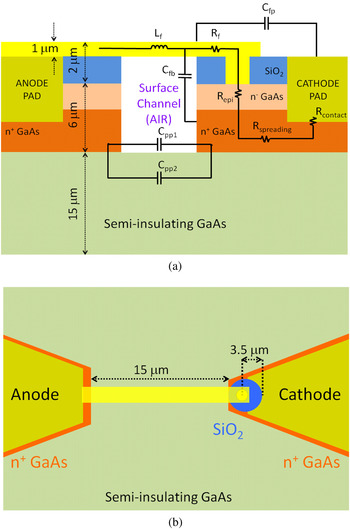
Fig. 1. A schematic of cross-sectional (a) and top view (b) of conventional surface-channel planar Schottky diode.
Table 1. List of different layer properties.

* Room temperature material properties are used in this analysis.
Total parasitic capacitance (C p ) is comprised of two parts: finger capacitance (C f ) and pad capacitance (C pp ). Pad capacitance is much more dominant than finger-induced capacitances due to smaller area associated with the finger. Therefore, it is of great desire to minimize C pp as dominant factor in parasitic capacitances. As a simple idea, this capacitance can be decreased by reducing pad area, increasing pad separation, decreasing substrate dielectric constant and substrate thickness. However, all of these modifications are somehow impractical and induce several detrimental side effects in device performance. Pad dimensions are limited by considerations of handling and bonding by ohmic contact resistivity in which such small dimensions can make fabrication process tough and unrepeatable. Large pad spacing, in addition to increasing footprint, also leads to excessive inductance that is not desirable and such a long finger makes fabrication process more difficult. Finally, it should be noted that for such a high-speed application, a semiconductor with high mobility and high saturation electron velocity is a must. These factors are available in only couple of materials such as GaAs, InP, GaInAs, which all of them have a dielectric constants similar to that of GaAs substrate. The most effective solution for decreasing pad-to-pad capacitance is to reduce the substrate thickness; but to reduce this component, a significant reduction in substrate thickness is needed. Considering inherent brittleness of the GaAs wafers, such thinning will make situation worse in which difficulty in handling during the fabrication will be a disadvantage for this modification. The components of finger capacitance, C fb and C fp are employed to model the fringing fields of finger–buffer layer and finger–pad, respectively. C pp1 and C pp2 model electrical coupling between contact pads through air and semi-insulating GaAs substrate, respectively. A series inductance, L f , is used to represent magnetic coupling through the finger.
In Fig. 2, we present a design with an improved structure. We propose etching a deep trench between electrical pads through semi-insulting GaAs substrate to reduce parasitic capacitances. We also propose using a closed-loop junction for reducing series resistance. In the following sections, we demonstrate that a higher cut-off frequency surface-channel planar Schottky diode operating at THz frequencies can be achieved by the proposed design.
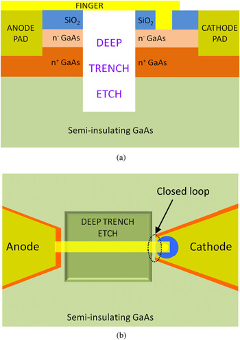
Fig. 2. A schematic of cross-sectional (a) and top view (b) of proposed surface-channel planar Schottky diode where closed-loop junction is indicated around the junction.
III. A THREE-DIMENSIONAL (3D) FULL-WAVE EM APPROACH AND LUMPED EQUIVALENT CIRCUIT
In order to have a better understanding of the effect of different geometries on parasitic elements and losses, a systematic modeling and analysis approach is required. In this approach, the Schottky diode structure is simulated in HFSS and results of this electromagnetic simulation is used for lumped equivalent circuit extraction in Microwave Office environment. For electromagnetic simulation setup, the discrete planar Schottky diode is attached on a finite ground CPW (Fig. 3) and excited with a lumped port. A 50 Ω CPW on a GaAs substrate (ε r = 12.9) is designed with a 30-μm-wide signal line and a gap of 21 µm inside an air box with surrounding radiation boundary. Unlike previous proposed modeling, which was based on rectangular waveguide [Reference Tang and Stake13], our modeling approach gives a more realistic estimation of the diode performance by monolithically implementing the Schottky diode integrated along the signal line of the CPW. Following the electromagnetic simulation of this structure in the frequency range of 150–600 GHz, S-parameter results are de-embedded by using thru-reflect-line technique [Reference Marks24], and they are used for parameter extraction for equivalent circuit model.
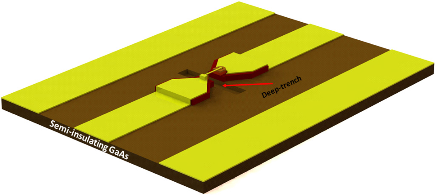
Fig. 3. Configuration of proposed planar Schottky diode attached to CPW line.
Figure 4 shows the equivalent circuit for the integrated CPW-diode structure. The effect of R epi is ignored since the current spreading in this layer is negligible. The n + buffer layer is heavily doped compared with the active epilayer, such that current flows straight down from the anode through the epilayer and spreads in the n + buffer layer. We also consider the finger as a perfect electrical conductor (PEC), so the effect of R f is ignored, as well. In this study, three cases are simulated: (i) open-lossless, (ii) short-lossless, and (iii) short-lossy. In lossless cases, both anode and cathode buffers are assumed as PECs, and in lossy case, the n + buffer layer is assumed to be doped with an electron concentration of 5 × 1018 cm−3. Open case also means that there is no contact between finger and buffer layers, and in short case, finger and buffer layers are short-circuited. The electromagnetic simulation results of the open-lossless case, where the diode is replaced with an open circuit and the n + buffer layer is assumed to be PEC, are used to extract the total capacitance using (2). Total inductance and also series resistance are estimated from short circuit simulations for lossless and lossy cases, respectively, according to (3) and (4).
 $$\eqalign{C_P & = C_{PP +} C_f \cr & = \left\{ {\displaystyle{1 \over \omega} \displaystyle{{{[{\rm image}( - Y_{12})]}^2 + {[{\rm real}( - Y_{12})]}^2} \over {{\rm image}( - Y_{12})}}} \right\}_{{\rm open} - {\rm lossless}},}$$
 $$\eqalign{L_{tot} & = L_{f} + L_a + L_c \cr & = \left\{ {\displaystyle{1 \over \omega} \displaystyle{{[{\rm image}(Y_{12})]} \over {{[{\rm image}(Y_{12})]}^2 + {[{\rm real} (Y_{12})]}^2}}} \right\}_{{\rm short} - {\rm lossless}},}$$
 $$\eqalign{R_S & = \left\{ {\displaystyle{1 \over \omega} \displaystyle{{[{\rm real}(Y_{12})]} \over {{[{\rm image(}Y_{12}{\rm )}]}^2 + {[{\rm real\;} (Y_{12})]}^2}}} \right\}{\rm \;} _{{\rm short} - {\rm lossy}} \cr &\quad - \left\{ {\displaystyle{{[{\rm real}(Y_{12})]} \over {{[{\rm image}(Y_{12})]}^2 + {[{\rm real\;} (Y_{12})]}^2}}} \right\}{\rm \;} _{{\rm short} - {\rm lossless}}.} $$
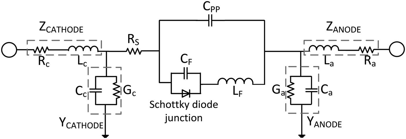
Fig. 4. The lumped equivalent circuit for our Schottky diode.
These starting values for C p , L tot , and R s are used to fine-tune the equivalent circuit in Microwave Office for the whole frequency range (150–600 GHz). This way, accurate values for each equivalent circuit parameter (C pp , C f , L f , L a , L c , and R s ) are extracted. In the next section, we provide a comprehensive study about the effects of different geometry-dependent elements. Initial dimensions for our simulations have been shown in Fig. 1.
IV. A THREE-DIMENSIONAL FULL-WAVE EM APPROACH AND LUMPED EQUIVALENT CIRCUIT
After introducing a systematic method for analyzing our Schottky diode based on electromagnetic simulations, in this section we investigate the effects of different geometrical parameters of the diode on parasitic and resistive elements. Based on the simulation results, a performance-enhanced Schottky diode structure is proposed. Finally, to verify the validity of the proposed idea, a scaled version of the diode is designed, fabricated, and characterized.
A) Parasitic capacitances
Table 2 gives the physical parameters of the diodes analyzed in the simulations. According to Fig. 1, total parasitic capacitance (C p ) can be divided into two parts: pad-to-pad capacitance C pp (including C pp1 and C pp2 ) and finger capacitance C f (including finger-to-pad C fp and finger-to-buffer C fb ). As it can be seen from Fig. 5, contribution from the pad-to-pad capacitance is dominant (especially in higher frequencies). Therefore, as mentioned above, it is desirable to minimize C pp which can be decreased by reducing pad area, increasing pad separation, decreasing substrate dielectric constant and substrate thickness. However, pad dimensions are limited by considerations of handling and bonding by ohmic contact resistivity [Reference Crowe, William, Bishop, Meiburg and Mattlauch15]. Large pad spacing, in addition to increasing footprint, also leads to excessive inductance that is not desirable [Reference Rizzi, Hesler, Dossal and Crowe25]. Thus, the most effective solution for decreasing pad-to-pad capacitance is to reduce the substrate thickness. Figure 6 plots C p for different substrate thicknesses. According to these results, by increasing substrate thickness, capacitance increases significantly, especially at higher frequencies. The frequency dependency becomes emphasized as the wavelength gets comparable with the physical device dimensions. Since the main goal of these simulations is to understand the impact of different geometries in device performance, in all parametric studies, substrate thickness is fixed at 15 µm. It should be noted that finger capacitance can also be reduced by decreasing the finger area, increasing the separation between finger and underlying conductive material, and reducing the passivation layer thickness that are depended to fabrication possibilities [Reference Crowe, Member, Matmuch, Roser, Bishop and Liu26, Reference Bishop, Crowe and Mattauch27].
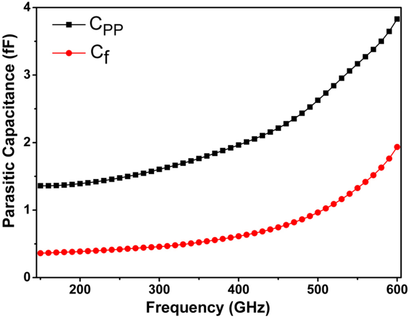
Fig. 5. Pad-to-pad and finger capacitances as a function of frequency for substrate thickness of 15 µm.
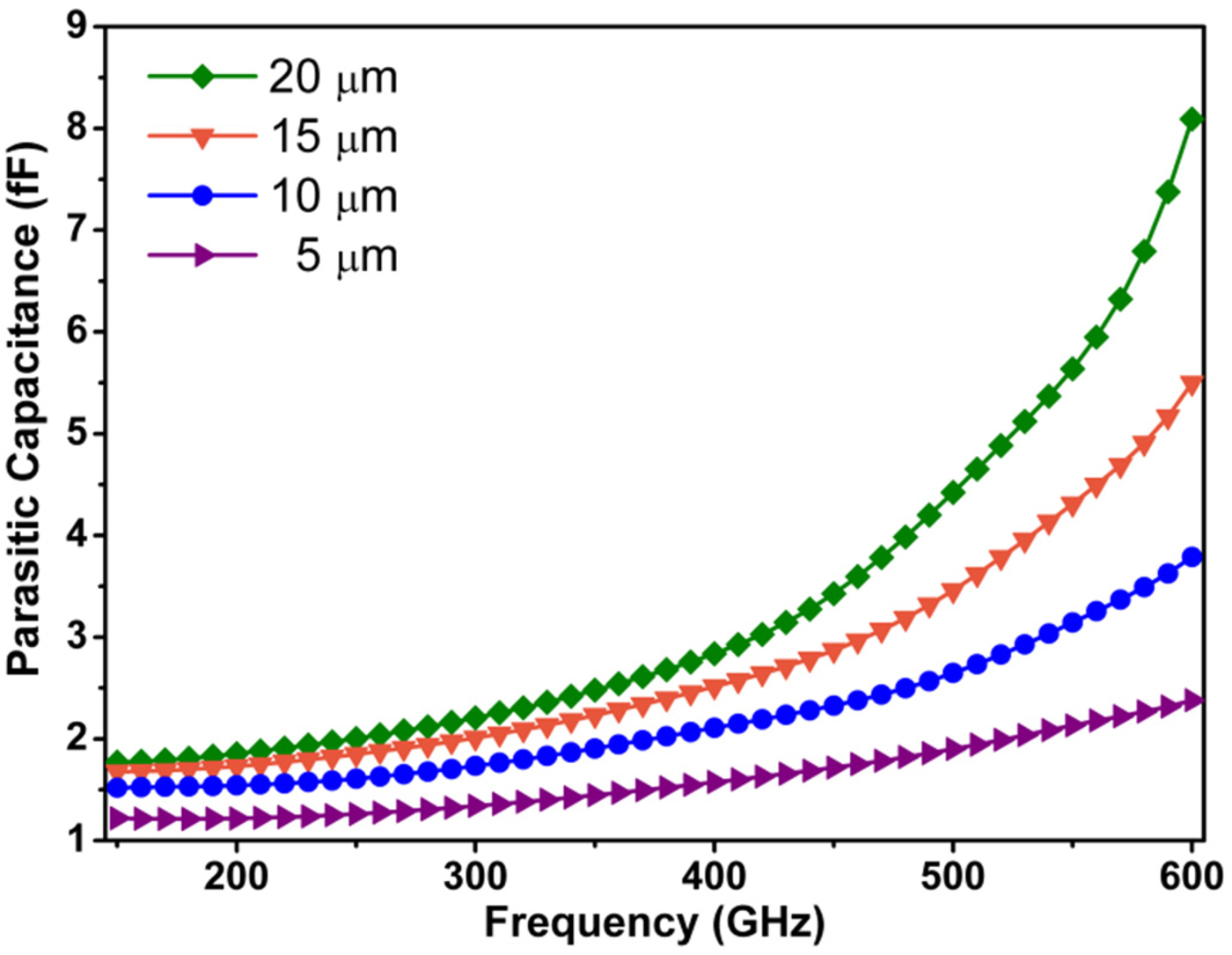
Fig. 6. Effect of substrate thickness on parasitic capacitance. By increasing substrate thickness, capacitance increases significantly, especially at higher frequencies.
Table 2. Physical parameters of the diodes analyzed in the simulations.

* Room temperature material properties are used in this analysis.
B) Spreading resistance
Another factor that degrades Schottky diode performance is spreading resistance (R spreading ). The finite conductance of the buffer layer results in current crowding and only a portion of total current can be collected at the ohmic contact. This loss is modeled by a resistor, R spreading , in the equivalent circuit model. The only geometric parameter that affects spreading resistance is the buffer layer thickness. Figure 7 plots spreading resistance values at different frequencies for different buffer layer thicknesses. As it is observed in [Reference Tang17], high-frequency spreading resistance exhibits a weak minimum at buffer layer thicknesses close to skin depth (that in this case it is approximately 1.7 µm at 600 GHz).
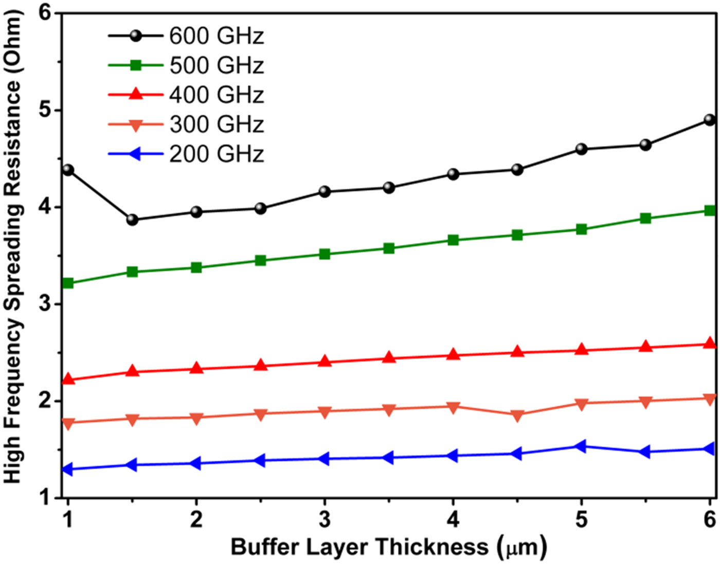
Fig. 7. The high-frequency spreading resistance as a function of buffer layer thickness.
C) Performance-enhanced Schottky diode
In this part, a performance-enhanced Schottky diode is proposed. C pp , the dominant shunt capacitance contribution to total parasitic capacitance, is composed of two parts: the shunt capacitance between the pads distributed across (a) a low permittivity region (air), C pp1 , and a high permittivity (GaAs) substrate, C pp2 . In addition to introducing a higher capacitance due to higher permittivity of the substrate (C pp2 > C pp1 ), C pp2 has greater frequency dependency and increases considerably with frequency. The parasitic capacitance can be reduced significantly by introducing a deep trench in the substrate between the two electrical contact pads (Fig. 8). For an etch depth equal to the substrate thickness, total parasitic capacitance (C p ) is minimized to <2 fF and relatively independent of the operation frequency and substrate thickness.
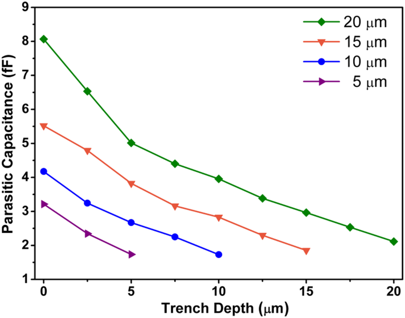
Fig. 8. Effect of trench depth on reduction of parasitic capacitance for different substrate thicknesses.
Another parameter that limits planar Schottky diode performance is the spreading resistance. Lateral current flow in the planar structure together with partially closed-loop junction in which just a portion of current will be collected with the ohmic contact. High-frequency current crowding phenomena such as eddy current and current crowding due to skin and proximity effects will add a new loss for lateral current flow in the buffer, and this loss is mainly dissipated as heat inducing a substantial increase in the amount of spreading resistance. Recently, it was investigated that the magnetic field couplings induced by the time-varying current in the air-bridge finger leads to the findings that links the high-frequency losses to the eddy current, and a mixture of skin and proximity effects [Reference Tang and Stake13]. According to the Faraday's law, AC voltage induced in a conductor is a result of time-varying magnetic field. The induced voltage then forces eddy current to circulate in a closed path within the conductor. According to Lenz's law, this induced modification in current flow, which is called eddy current, generates its own magnetic field to oppose the original magnetic field. The circulation of eddy current results in a non-uniform current density distribution (current crowding) and consequently will increase power loss associated with current flow. In order to reduce R spreading , we propose a closed-loop junction to collect radial current in all directions. Figure 9 compares the simulation results for conventional and closed-loop junctions. As it can be clearly seen, in the whole frequency range the spreading resistance is reduced by a factor of around two. By taking the value of the zero-bias junction capacitance (2.5 fF) from the earlier reports of the fabricated planar Schottky diode structure [Reference Crowe, Member, Matmuch, Roser, Bishop and Liu26–Reference Kiuru30], we can estimate the cut-off frequency of the conventional and performance-enhanced Schottky diodes. The cut-off frequency of the conventional structure is found to be 4.1 THz, while that of the enhanced structure presented in this work is 14.1 THz (these numbers are calculated using series resistance and parasitic capacitance values at 600 GHz). Parasitic capacitance and series resistance values at 600 GHz have been chosen for this calculation. This approach to determine the cut-off frequency is validated at a lower operation frequency (40 GHz).
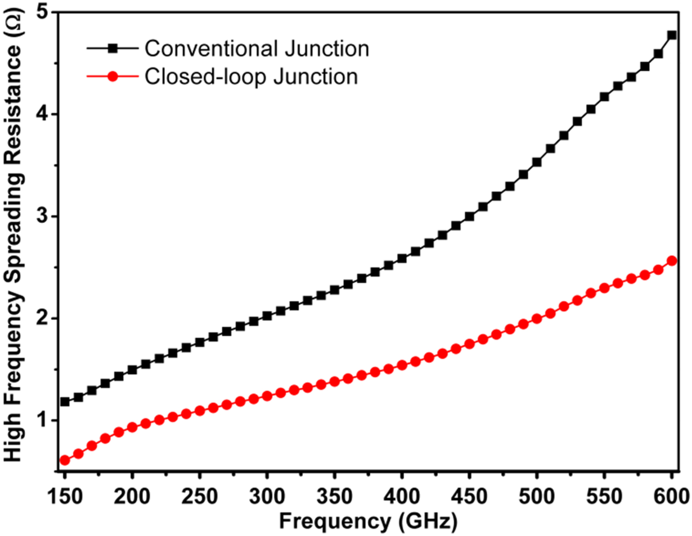
Fig. 9. Effect of closed-loop junction on reduction of high-frequency spreading resistance. The spreading resistance is reduced by a factor of around two with the use of a closed-loop junction.
D) Fabrication and characterization of performance-enhanced Schottky diode
To verify the accuracy of this modeling approach, a scaled version of the planar THz Schottky diode has been designed, fabricated, and characterized. Considering the available fabrication, measurement and RF probing capability, our modeling approach is validated with experiments up to 40 GHz. At this frequency, 500 µm-thick GaAs substrate is sufficiently thin since the substrate modes are not excited. Figures 10(a) and 10(b) show scanning electron microscope (SEM) image of the fabricated diode. As it can be clearly seen, the fabricated diode that has a diameter of 5 µm has been integrated to a 50 Ω CPW line. The width of the trench (the size that is perpendicular to the finger) is longer than the ones used in the simulations. As a design rule, it is sufficient to have 10 times the finger width. The reason for fabricating larger trenches extending from finger toward the ground is to be able to reduce the risk of misalignment in the photolithography step of the diode fabrication. The fabrication steps of the diode are summarized as follows: The epitaxial GaAs wafer with a 4 µm-thick heavily doped n + layer and 250 nm thick n − layer above is grown on a 500 µm-thick semi-insulating GaAs substrate using molecular beam epitaxy (MBE). The doping concentrations of n + and n − layers are 5 × 10¹⁸ and 1 × 1017 cm−3, respectively. First of all, a 200 nm-thick SiO2 isolation layer is deposited using plasma-enhanced chemical vapor deposition and patterned using buffered oxide etching process. Afterward, n − layer is etched away through the wet etching process from the whole wafer apart from the Schottky contact area. To this end, a solution of NH4OH : H2O2 : H2O (28 : 5 : 200) is utilized to etch the layer with an etch rate of 4.2 nm/s. As the ohmic contact, an alloy of Ge/Ni/Au (10 nm/10 nm/150 nm) is deposited employing thermal evaporation, annealed at 450 °C for 45 s using rapid thermal annealing and finally patterned with a lift-off process. Prior to formation of finger and CPW line, the n + layer is totally removed using the same etchant, while only the n− layer and areas under the ohmic contacts are masked. The next step is the formation of finger and CPW line using a 150 nm-thick evaporated Au layer followed by a lift-off process. In the last step, the n + layer beneath the air-bridge finger is etched away using the same wet etching process in order to isolate the anode and cathode ohmic pads. After this step, 5 µm-deep trench is formed through the semi-insulating layer to verify the applicability of the proposed idea in the reduction of the diode parasitic capacitance.
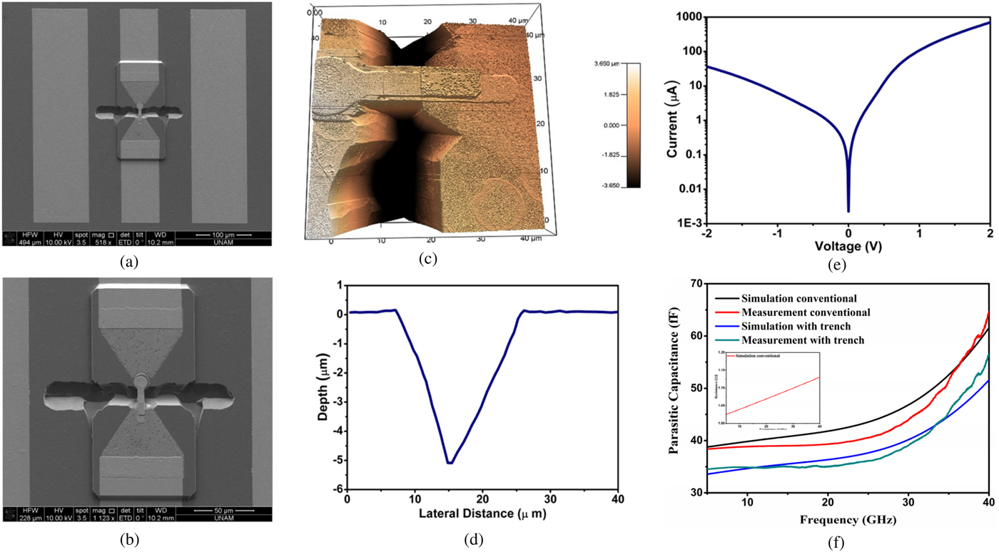
Fig. 10. (a, b) SEM images, (c, d) 3D and 2D AFM images, (e) IV characteristics, and (f) extracted high-frequency capacitances of the Schottky diode. The diode resistance extracted from simulations is given as the inset.
In order to assess the etching profile of the fabricated diodes, 3D and 2D atomic force microscopy (AFM) measurements have been conducted on the sample, as shown in Figs 10(c) and 10(d). The measured profile has been employed to get more accurate simulation results from modeling approach. On the other hand, DC I–V characteristic of the diode illustrates the diode behavior of the fabricated device (Fig 10(e)). Finally, high-frequency capacitance of the fabricated and simulated diodes have been extracted and compared in Fig 10(f). The inset plot shows the diode resistance extracted from simulations where the buffer layer is assumed to be lossless. It should be noted that the diode measured is 10 times larger than the original THz diode to be able to employ the 40 GHz probes and probe station. Due to the scaling of the physical size, the capacitance values in Fig. 10(f) is much larger than the ones Fig. 8. As this figure shows, the introduction of the deep trench reduces the parasitic capacitance of the diode for both simulation and measurement results. The simulation and measurement results have a good agreement particularly at low frequencies. Although the details for the etching profile are included in the simulation geometry, for the higher frequencies, the agreement is lower. This mismatch is mainly due to inaccuracies in geometries of the simulation setup where the impact of these geometrical differences is much more pronounced in higher frequencies. It should be noted here that the trench is overetched in the lateral direction. It is expected to have about 5 µm of undercut in the lateral direction as the depth of the trench is also about 5 µm. However, the lateral etched size is 15 µm, which can be related with the quality of the epi-layer. When exposed to wet etching, scoops of epi-layer are etched in lateral direction while the sample is still immersed to achieve sufficient trench etch. The etching profile can be improved and a rectangular trench geometry can be achieved by developing dry etching recipes.
V. CONCLUSION
In this paper, we demonstrate a performance-enhanced planar Schottky diode for THz applications using a hybrid electromagnetic and circuit modeling approach. Based on this modeling approach, a parametric study is carried out to investigate the relationship between the physical parameters of the diode and parasitic elements, which limit the device cut-off frequency. The improved design features a deep trench in the substrate between electrical pads and a closed-loop junction, which reduces the parasitic capacitance and series resistance, respectively. Finally a scaled version of the diode was designed, fabricated, and characterized to verify the validity of the deep-trench idea. The methodology presented here provides a good estimate of diode impedance, which might be used to design monolithically integrated detectors where THz antenna impedance is conjugate-matched to the Schottky diode impedance to increase detector sensitivity.
ACKNOWLEDGEMENT
This work was supported in part by European Union Framework Program 7 Marie Curie IRG under Grant 239444 and Grant 249196, by the COST NanoTP, and by The Scientific and Technological Research Council of Turkey (TUBITAK) under Grants 109E044, 112M004, 112E052, 112M482, and 113E126. The authors would like to thank Dr. Bulent Aslan for MBE process.
 Amir Ghobadi was born in Tehran, Iran, in 1989. He received the B.S. degree in Electrical Engineering from the University of Tehran, Tehran, in 2012. He has received the M.S. degree in Electrical Engineering from Bilkent University. He is currently working toward the Ph.D. degree in the Department of Electrical and Electronics Engineering at Bilkent University, Turkey. His research involves on the design, synthesis, and characterization of novel semiconductor-based photovoltaic devices.
 Talha Masood Khan was born in Pakistan, in 1989. He received the B.E. degree in Electronics Engineering from the Bahauddin Zakariya University (BZU), Multan, Pakistan, in 2011, and M.S. degree in Electrical Engineering from the National University of Sciences and Technology (NUST), Islamabad, Pakistan, in 2013. From 2013–2014, he joined the Department of Electrical Engineering, Pakistan Institute of Engineering and Technology (PIET), Multan, Pakistan, as a Lecturer, and served as a Visiting Lecturer at BZU, Pakistan. Since September 2014, he joined Bilkent University, Ankara, Turkey as Ph.D. candidate at the Institute of Material Sciences and Nanotechnology (UNAM) and has been working in the field of THz antennas, Bio-MEMS design, and fabrication. Mr. Khan is a member of Pakistan Engineering Council (PEC) and student member of IEEE and SPIE.
 Ozan Onur Celik received the B.S. degree in Electrical and Electronics Engineering from the Bilkent University in 2014 and currently is a senior M.S student in the same university. His Master's thesis is on flexible VCO-IP generation using submicron CMOS technologies and his research interests include microwave/RF devices fabrication and circuit design.
 Necmi Biyikli was born in Utrecht, The Netherlands, in 1974. He received the B.S., M.S., and Ph.D. degrees in Electrical and Electronics Engineering from the Bilkent University, Ankara, Turkey in 1996, 1998, and 2004, respectively. Dr. Bıyıklı’s Ph.D. research concentrated on GaN/AlGaN-based ultraviolet and solar-blind photodetectors. Afterwards, during his post-doctoral research at the Virginia Commonwealth University, he worked on the MOCVD growth of AlGaN/GaN heterostructures for various applications including high-performance transistors. Dr. Bıyıklı also worked as a research scientist at the Cornell Nanoscale Science and Technology Facility (CNF) where he developed RF-MEMS integrated multifunctional reconfigurable antennas. Since 2008, he is with the UNAM – Materials Science and Nanotechnology Institute at the Bilkent University, leading the “Functional Semiconductor Materials and Devices Research Group”. His current research interests include atomic layer deposition of III-Nitride and metal-oxide thin films and nanostructures, III-Nitride opto-electronics, piezo-electric thin films for chemical and biological sensing, photo-voltaics, biosensors, microfluidic analysis systems, and smart RF-antenna architectures. He is the author of over 100 citation-index journal papers and refereed conference proceedings.
 Ali Kemal Okyay received his B.S. in EEE from the Middle East Technical University in 2001. He got his M.S. and Ph.D. degrees in EEE from the Stanford University in 2003 and 2007, respectively. He joined as an Assistant Professor in EEE, Bilkent University, in 2008. He is currently an Associate Member of the UNAM-National Nanotechnology Research Center, Institute of Materials Science and Nanotechnology. His research focuses on integrated devices for functional and smart systems.
 Kagan Topalli was born in 1979. He received B.S. and Ph.D. degrees in Electrical and Electronics Engineering from the Middle East Technical University (METU), Ankara, Turkey, in 2001 and 2007, respectively. Between 2001 and 2007, he has worked as a Research Assistant at METU in the Department of Electrical and Electronics Engineering. Between 2007 and 2010, he has worked as a Research Engineer at the METU-MEMS (MicroElectroMechanical Systems) Center. Dr. Topalli worked as a post-doctoral researcher at the ElectroScience Laboratory of the Ohio State University between February 2010 and February 2012. He worked as a faculty at the TED University, Department of Electrical and Electronics Engineering in Ankara, Turkey between February 2012 and May 2014. Dr. Topalli worked as a faculty at the Bilkent University, National Nanotechnology Research Center (UNAM), Institute of Materials Science and Nanotechnology between May 2014 and September 2016. He is currently working as a Chief Research Scientist at the TUBITAK-Space Technologies Research Institute. Dr. Topalli's recent research interests include THz sensors and THz imaging systems. He has also conducted research on the development, characterization, and integration of novel RF MEMS structures for RF front ends at microwave and millimeter-wave, reconfigurable antennas, phased arrays, microwave packaging, and microfabrication technologies. Dr. Topalli received the “METU Thesis of the Year Award” in 2007 for his Ph.D. dissertation, which was awarded by the Prof. Mustafa N. Parlar Education and Research Foundation. He received the “URSI (Union of Radio Science-International) Young Scientist Award” in 2011. He received “Research Incentive Award” in 2013 given by the Prof. Mustafa N. Parlar Education and Research Foundation. He is the co-advisor to the recipient of “METU Thesis of the Year Award” in 2015. He is a senior member of IEEE.


