I. INTRODUCTION
Ultra-wideband (UWB) technology was mainly used for military and radar applications. In recent times, it is widely utilized for ambit of short-range high-throughput wireless communications, medical imaging, ad hoc networking, high-resolution, reliable data, low-power consumption, high immunity to multipath interferences, high channel capacity, and high security measures. Fork-shaped radiating patch and the U-shaped monopole results in dual band-notched characteristics with desired bandwidth, which resonates over the Bluetooth and UWB band [Reference Mishra, Gupta, Vaidya and Mukherjee1]. Through inverted-T slot and pair of C-shaped parasitic element near the feed line or arc-shape stepped rectangular patch connected to the microstrip feed line on the top side of the substrate for dual band-notched characteristics of monopole UWB antenna [Reference Jiang and Che2, Reference Nouri and Dadashzadeh3]. V-shaped protruded strip on the ground plane and L–E-shaped slot on the radiating patch is responsible for resonances at high frequency. By controlling folded T-shaped element (FTSE) on the fractal radiating patch and the number of fractal unit are responsible for band-notch features. Moreover, promising mechanical and thermal properties of thermoplastic acrylonitrile butadiene styrene polycarbonate substrate has been reported for integration in molded interconnects devices technology [Reference Mehranpur, Nourinia, Ghobadi and Ojaroudi4–Reference Unnikrishnan, Kaddour, Tedjini, Bihar and Saadaoui6]. A stable linear polarization (29 × 43 mm2) is developed by introducing a ground cooperative radiating structure into the metal ground of a prototype defected hexagonal monopole antenna [Reference Zhao, Yang, Zhu and Chen7]. Two elliptical slots on radiating circular ring with parasitic elements near the feed line are reported for triple band-notch configuration. Multimode-resonator filter consisting of a single-wing element is combined with the modified slot UWB antenna providing a 6 dB increase in the realized gain near 10 GHz. In monopole dual band-notched antenna, C–T-shaped slot on the radiating patch enhanced the bandwidth by 125%. Chamfered edges at the bottom of radiating patch and a slit in the ground plane improves impedance matching and by variation of T-shape stub length, high band rejection, and wide radiating patterns are obtained. Structural modification in the radiating fins of Vivaldi antenna has increased the electrical length thereby reducing the lower operating frequency from 5.2 to 3.7 GHz and antenna maintain −20 dB co-polarization to cross-polarization ratio throughout the bandwidth [Reference Srivastava, Dwari and Kanaujia8–Reference Natarajan, George, Kanagasabai and Shrivastav12]. Multiple wireless applications including UWB with triple band notch characteristics is reported and WiMAX notch is achieved by inverted T-shape stub without elimination of C-band (3.80–4.20 GHz). It is also observed that there is more power coupled between two C-shaped slots for notched bands due to which it is difficult to control them separately and at higher frequencies, radiation pattern shows more cross-polarization [Reference Sharma, Awasthi, Singh, Kumar and Kumari13]. As discussed in [Reference Pandey, Singh, Bharti and Meshram14–Reference Pandey, Singh, Bharti and Meshram16], antenna is characterized based on equivalent circuit model. Furthermore, beak-shaped monopole-like antenna also reported with enhanced bandwidth for GPS (1.52–1.59 GHz), GSM (1.77–1.84 GHz), and Bluetooth (2.385–2.490 GHz). Dual notch-band is obtained by electromagnetically coupling between a coupled inverted U-ring strip and cross shaped radiating patch beside fork-shaped slit in the ground with antenna dimension 12 × 18 mm2 [Reference Chandel, Gautam and Kanaujia17–Reference Verma, Awasthi and Singh19]. Electromagnetic coupling theory can create band-notch functions by butterfly-shape parasitic element on backplane of radiating patch and 155% bandwidth enhancement is achieved by rectangular-shaped slots on ground plane [Reference Beigi, Nourinia, Mohammadi and Valizade20]. Flower shape [Reference Sharma, Awasthi, Singh, Kumar and Kumari21] dual band-notch fractal antenna is obtained by embedding smaller 20 circles on conventional UWB circular radiating patch for enhancement of bandwidth. Antenna is fabricated on a FR4 substrate with low rejection at notched bands, which will not suppress interference to some extent. S-shaped multi frequency patch antenna exhibits stable gain, omni-directional radiation pattern and constant efficiency makes it suitable for X-band applications [Reference Samsuzzaman and Islam22]. TCDA (tightly coupled dipole array) is capable of operating in upper S, C, X, and Ku bands (3–18 GHz). In [Reference Bhattacharya, Roy, Islam, Chowdhury and Bhattacharjee23], hexagonal patch structure is capable of working in X-band (8–12 GHz) and Ku-band (12–18 GHz). In [Reference Naghar, Aghzout, Essaaidi, Alejos, Sanchez and Falcone24], planar low-cost antenna is reported for C, X, and Ku band applications. UWB conical monopole antenna is capable for applications in Wi-Fi, Bluetooth, WiMAX, Bluetooth 4.0 Wireless, X-band, and Ku band applications [Reference Yeoh and Rowe25].
In this paper, a dual band-notch small monopole antenna with 20 × 20 × 0.787 mm3 is proposed. Vase-shape radiating provides a measured wider bandwidth (2.58–20.39 GHz) with dual band-notch characteristics along high band-rejection centered at 3.77 GHz (VSWR = 25.33) and 5.64 GHz (VSWR = 5.78) and also convenient for multiple wireless service, including close range radar: 8–12 GHz in X-band and satellite communication: 12–18 GHz in Ku band. The performance of proposed antenna is also compared with previous designed antennas.
II. ANTENNA DESIGN
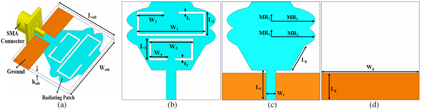
The proposed planar monopole antenna fed by 50 Ω microstrip line is shown in Fig. 1(a). The antenna is fabricated on Rogers RTDuroid5870 substrate of thickness 0.787 mm with relative permittivity ε r = 2.33, tanδ = 0.0012. Radiating patch comprises of basic hexagonal shape with each optimized side of 8.0 mm. Side of hexagonal patch designated as L p is calculated by
 $$L_p = \displaystyle{c \over {4 \times f}}\sqrt {\displaystyle{2 \over {1 + \varepsilon _{reff}}}}, $$
where f is the operating frequency and c is the speed of light in free space, i.e. 3 × 10⁸ m/s. In order to enhance bandwidth, two ellipses with major radius of 9.0 mm and eccentricity ratio of 0.33 are embedded on hexagonal patch and optimized antenna to obtain wider bandwidth as shown in Fig. 1(c). As shown in Fig. 1(b), radiating patch consists of two C-shaped slot, which are responsible for WiMAX/C-band notch (3.3–4.2 GHz) and WLAN band notch (5.15–5.825 GHz). At the notched frequency, the current is mainly distributed on the exterior and interior edges of the slots. As a result, the desired high attenuation near the notch frequency is produced. Figure 1(d) shows rectangular ground plane with optimized dimensions. The parameters of proposed antenna are optimized using electromagnetic (EM) high-frequency structural simulation. The length of the first and second notches is calculated by using equations (2) and (3) and widths of notches are optimized arbitrary:
 $$L_{{\rm Notch}\;{\rm Band}} = \displaystyle{c \over {(2 \times f_{FirstNotch} \sqrt {\varepsilon _{reff}} )}},$$
 $$\varepsilon _{reff} = \displaystyle{{\varepsilon _r + 1} \over 2} + \displaystyle{{\varepsilon _r - 1} \over 2}\left[ {1 + 12\displaystyle{{h_{sub}} \over {W_f}}} \right]^{^{ - 1/2}}. $$

Fig. 1. Geometry of the proposed UWB antenna with notched bands. (a) Slant view, (b) front view with dual notch, (c) front view, (d) back view.
From [Reference Verma, Awasthi and Singh19], effective relative permittivity of substrate is calculated ε reff (w f /h sub , εr, f). The optimal dimensions of the designed antenna are as follows: W sub = 20.0 mm, L sub = 20.0 mm, h sub = 0.787 mm, W f = 20.0 mm, L f = 6.0 mm, L p = 8.0 mm, MR1 = 9.0 mm, MR2 = 3.0 mm, W g = 20.0 mm, L g = 5.5 mm, t 1 = t 2 = 0.5 mm, L 1 = 5.0 mm, L 2 = 4.5 mm, W 1 = 14.0 mm, W 2 = 5.5 mm, W 3 = 9.0 mm, W 4 = 3.80 mm.
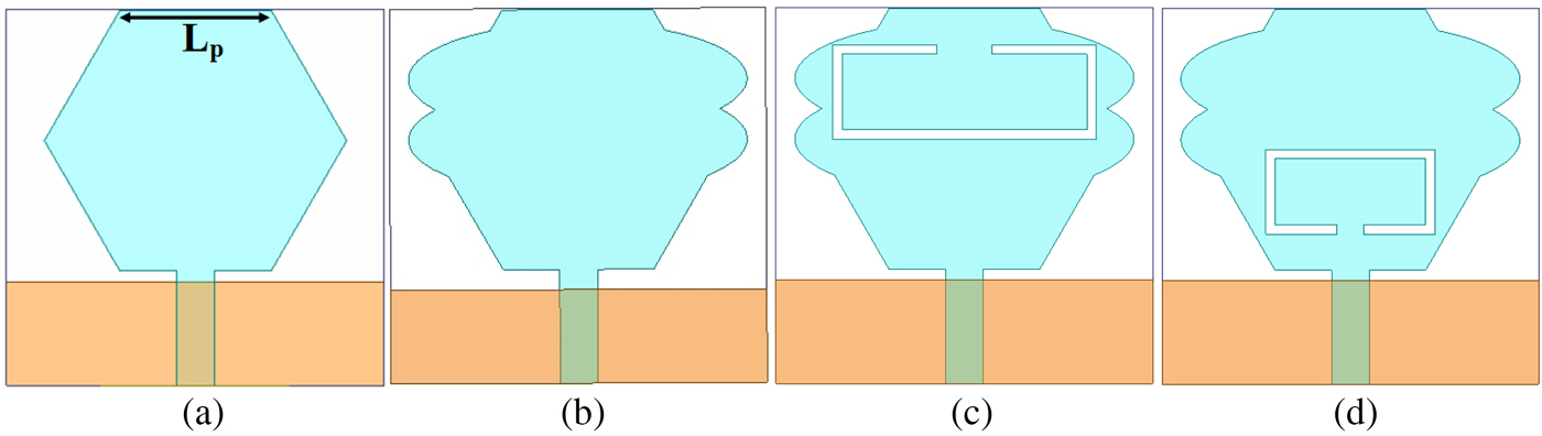
Figure 2 shows the configuration of proposed antennas used for multi-resonance and dual band-notch performance. Figure 3 shows the simulated VSWR plot in respective of Fig. 2. Antenna design starts with conventional hexagonal radiating patch shown in Fig. 2(a), where partial UWB bandwidth is obtained (3.63–10.23 GHz). As per FCC standard, UWB bandwidth is 7.5 GHz (3.1–10.6 GHz) intended. Therefore, enhancement of bandwidth is required, which obtained by proposed modification of radiating patch by embedding two ellipses with major radius of 9.0 mm each and eccentricity ratio of 0.33, forming proposed antenna with wider bandwidth covering 2.60–19.60 GHz, which is shown in Fig. 2(c) and corresponding VSWR results is shown in Fig. 3. With a C-shape slot on the radiation patch as shown in Fig. 2(c) results in removal of WiMAX/C-band from 3.21–4.30 GHz. WLAN band is eliminated by etching C-shape slot as shown in Fig. 2(d) eliminating 5.12–5.84 GHz. From Fig. 3, simulated proposed antenna shows high band rejection at 3.64 GHz with VSWR = 14.98 and 5.32 GHz with VSWR = 29.79.

Fig. 2. Monopole antenna with (a) partial UWB bandwidth, (b) UWB-extended bandwidth, (c) WiMAX/C notch, (d) WLAN notch.
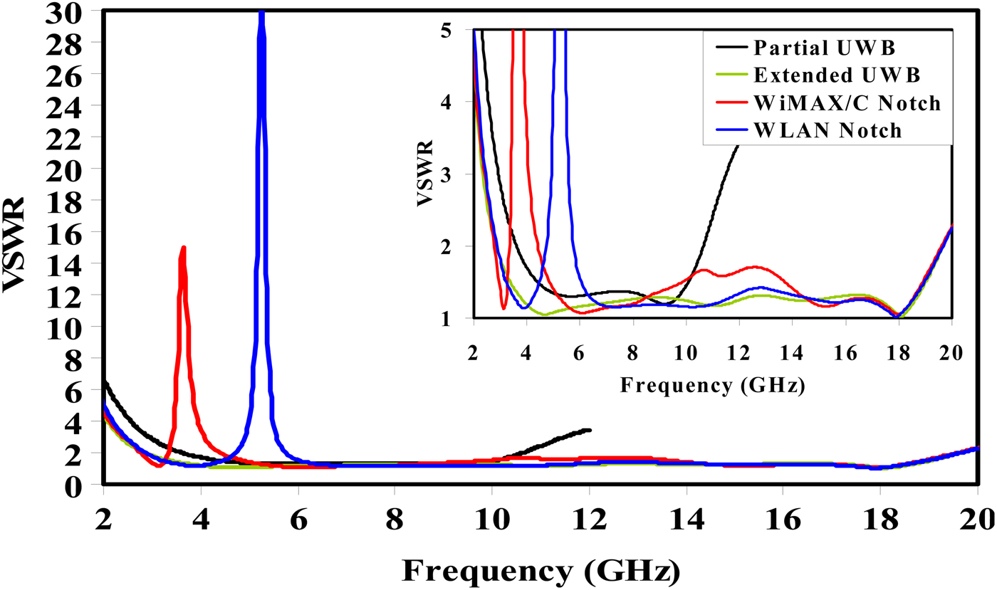
Fig. 3. VSWR results of partial UWB, UWB-extended, WiMAX/C, and WLAN notched bands antennas.
III. PARAMETRIC STUDY OF NOTCHED BANDS
The proposed antenna is optimized and investigated by full-wave finite element method solver. The center frequency of notched bands along with peak value of VSWR is controlled by the length of C-shaped slots, whereas bandwidth of notched bands are also controlled by width of slots, as discussed below:
-
(a) Effect of slot length W 2 & W 4
For the first notch, as shown in Fig. 4, centered at 3.45 GHz, length of the first slot is calculated as L WiMAX/C-Band = W 1 + 2(W 2 + L 1) mm. By varying W 2 from 4.50 to 6.50 mm, VSWR curve shifts from higher to lower frequency band. Also by optimizing W 2 = 5.50 mm desired WiMAX/C-band (3.20–4.31 GHz) is achieved. VSWR values at notch vary from 18.77 to 15.82. Impedance bandwidth in the entire band (2.26–19.60 GHz) is also maintained appreciably throughout optimization of W 2.
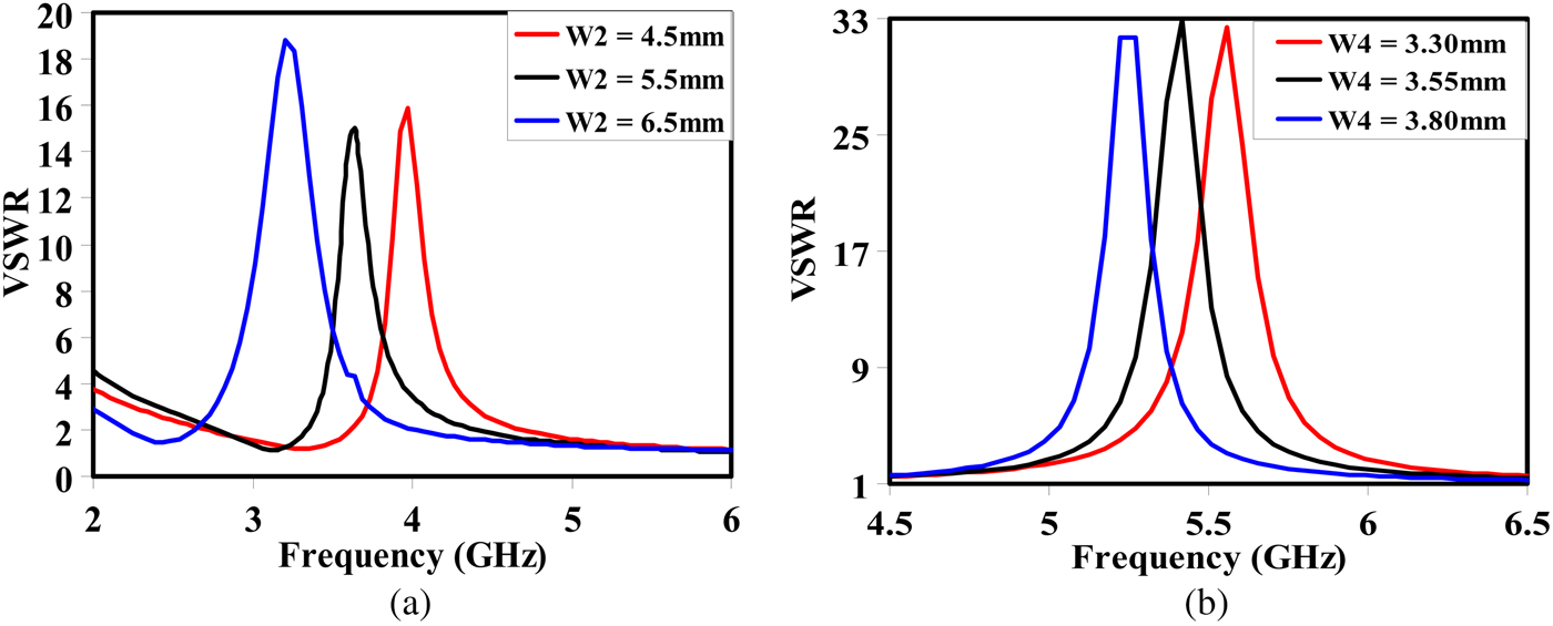
Fig. 4. Simulated parametric variation for (a) WiMAX/C (3.3–4.2 GHz) band, (b) WLAN (5.150–5.825 GHz) band.
Also for second notch as represented by Fig. 4, centered at 5.42 GHz, length of the second slot is calculated as L WLAN = W 3 + 2(W 4 + L 2) mm. By varying W 4 from 3.30 to 3.80 mm, VSWR curve shifts from higher to lower frequency band. Also by optimizing W 4 = 3.80 mm desired WLAN band (5.120–5.832 GHz) is achieved. VSWR values at notch vary from 32.92 to 2.44. Impedance bandwidth in the entire band (2.86–19.63 GHz) is also maintained appreciably throughout optimization of W 2.
-
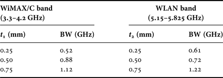
(b) Effect of slot width t 1 and t 2.
Table 1 represents variation of slot thickness t 1 and t 2. For WiMAX band, as slot thickness t 1 is varied from 0.25 to 0.75 mm, bandwidth varies from 0.52 to 1.12 GHz and for WLAN band, as slot thickness t 2 is varied from 0.25 to 0.75 mm, bandwidth varies from 0.61 to 1.22 GHz.
Table 1. Parametric variation of notched-bandwidth by varying width of slots (t 1 and t 2 as shown in Fig. 1(b)).
IV. SURFACE CURRENT DENSITY DISTRIBUTION, INPUT IMPEDANCE, TIME-DOMAIN ANALYSIS, AND EQUIVALENT CIRCUIT ANALYSIS
Furthermore, to understand the phenomenon behind dual notch performance, the simulated current distribution on the radiating patch for proposed antenna at the notched frequencies 3.45 and 5.42 GHz is carried out shown by Figs 5(a) and 5(b). It can be concluded from Figs 5(a) and 5(b) that the current is concentrated on the inner and outer edges of the C-shaped slots. Due to this there is change in impedance of proposed antenna.
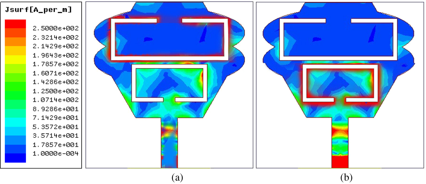
Fig. 5. Simulated current density distribution at (a) 3.45 GHz, (b) 5.42 GHz.
Moreover, the strong current distributions around slots at the notched frequency leads to near-field radiation counteracted, due to which high energy is reflected back to the input port and the band-notched characteristics are achieved. It is also noticed that in Figs 5(a) and 5(b) there are very low mutual coupling at notched frequencies, which indicate that each rejected band can be controlled independently. In addition, it is also observed that at entire frequency pass band except dual band-notch, the surface current is distributed uniformly over antenna.
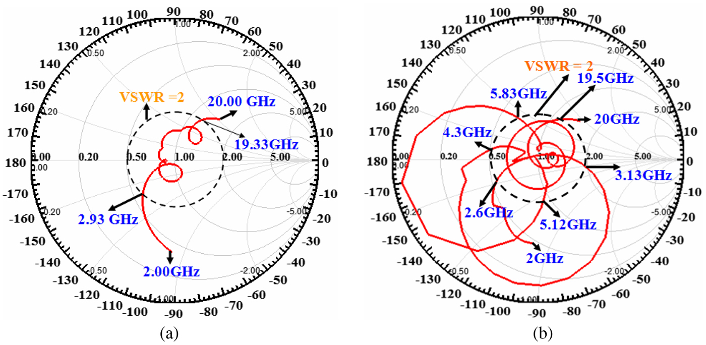
As shown in Fig. 6(a), simulated input impedance on smith chart represents for UWB antenna with extended bandwidth without notch bands covering UWB band from 2.93 to 19.33 GHz. Figure 6(b) represents multi-resonance planar monopole UWB antenna structure shown in Fig. 1(b) with dual band-notch. VSWR = 2.0 circle is drawn on the smith chart and it is clear that smith chart starts at 2.00 GHz and falls below VSWR = 2 at 2.60 GHz and comes out of VSWR = 2.0 circle at 3.13 GHz and re-enters at 4.30 GHz. From 3.13 to 4.30 GHz smith curve remains outside VSWR = 2.0 which confirms the elimination of first notch (3.30–4.20 GHz). Similarly at VSWR = 2.0 circle comes out at 5.19 GHz and re-enters at 5.83 GHz. From 5.19 to 5.83 GHz smith curve remains outside VSWR = 2.0, which confirms the elimination of second-notch (5.15–5.825 GHz). For remaining UWB band the smith curve is well below VSWR = 2.0. For VSWR = 2.0 proposed ordinary monopole UWB antenna covers 2.60 to 19.50 GHz. It is clear from the Smith chart that all the two notch bands for WiMAX (3.13–4.30 GHz), WLAN (5.19–5.83 GHz) are rejected.

Fig. 6. Simulated input impedance on Smith chart (a) UWB-extended bandwidth, (b) dual band-notch proposed antenna.
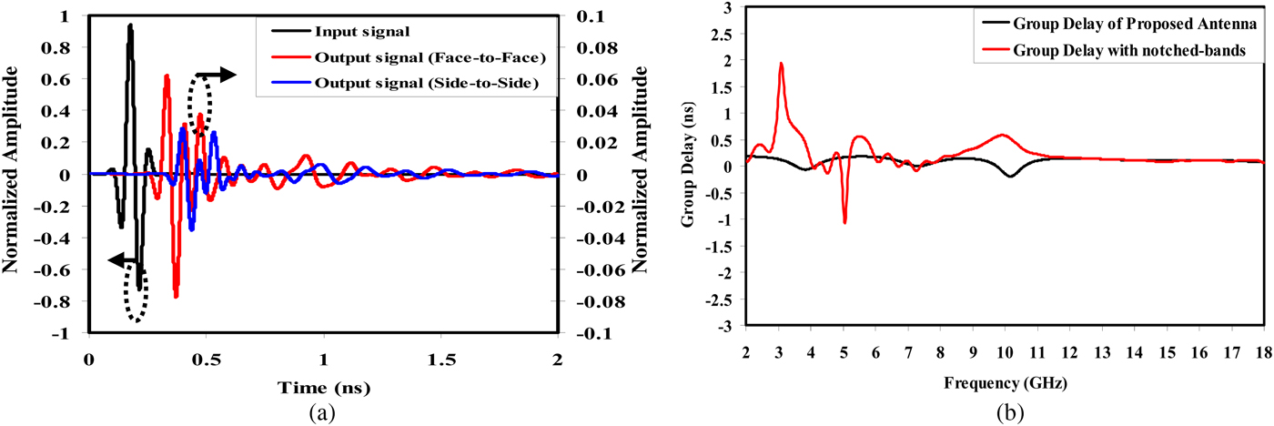
The simulated input signal and output signal for the proposed antenna is shown in Fig. 7(a). Pulse distortion, which is one of the characteristics of UWB signals is essentially determined by their wide bandwidth. To overcome minimize reflection loss and to avoid pulse distortion good impedance match has to be maintained throughout the operating band. The main reason between the signal distortion as shown in Fig. 7(a) is due to mismatch between source pulse and the antenna. As a result, some frequency components cannot be transmitted effectively by the monopole, leading to the distortions of the received signal. Figure 7(b) represents the group delay of proposed antenna without and with notched bands. Group delay is an important parameter for UWB and other communications since it can judge the distortion of transmitted pulses. For the perfect pulse transmission, the group delay should be closed to a constant within the entire band. It can be also concluded that the proposed antenna has perfect performance in this aspect, which makes it quite suitable for UWB as well as other high band wireless communication, which has been carried out by CST Microwave Studio (only for time-domain analysis).

Fig. 7. (a) Time-domain analysis of proposed antenna (input signal and output signals in face-to-face & side-to-side orientation). (b) Group delay of the proposed antenna without/with notched bands.
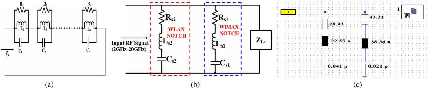
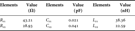
In order to analyze the theory behind UWB and triple notched band characteristics, equivalent circuit model based on input impedance response is carried out, which is obtained from full-wave EM solver. Based on input impedance characteristics, UWB antenna can be modeled as the result of several adjacent resonance circuits, which equally represents parallel RLC circuit [Reference Pandey, Singh, Bharti and Meshram14–Reference Pandey, Singh, Bharti and Meshram16] and equivalent circuit model based on the concept for UWB-extended bandwidth antenna is shown in Fig. 8(a).
 $$Z_{La} = \sum\limits_{j = 1}^n {\displaystyle{{j\omega R_j L_j} \over {R_j \;(1 - \omega ^2 L_j C_j ) + j\omega L_j}}}. $$

Fig. 8. Equivalent circuit model for (a) UWB-extended bandwidth antenna, (b) proposed antenna, (c) snapshot of the proposed antenna in CST design studio.
Either from simulated or measured results corresponding to resonances (Z La ), values of consecutive parameters of the equivalent circuit model are calculated (R j , Lj, Cj ) by equation (4). Figure 9(a) represents input impedance of antenna shown in Fig. 1(b). Real and imaginary parts of input impedance value vary about 50 and 0 Ω , respectively. In case of notched band characteristics (WiMAX/C & WLAN bands), high mismatch impedance is required, which is shown in Figs 8(b) and 8(c). In case of WiMAX/C band-notched band characteristics, at 3.50 GHz, real part of impedance is 1.6 Ω, whereas imaginary part of impedance shifts from negative to positive value, which corresponds to series resonance circuit. Corresponding series resonance circuit is represented in Fig. 8(b) and corresponding results are shown in Figs 9(b) and 9(c). In case of the WLAN band, real impedance value is 2.1 Ω at 5.25 GHz and corresponding imaginary impedance value shifts from negative to positive value leading to series RLC resonance circuit. For remaining UWB-extended bandwidth, real part of impedance varies about 50 Ω and imaginary part varies about 50 Ω. Also, VSWR curve is plotted for entire dual notched UWB antenna, which is compared by simulated and measured results represented in Fig. 10(a). At notched frequencies, either open or short (high- or low-input impedance) at the antenna input terminals results in mismatch from 50 Ω impedance and large reflections at input and band notch characteristics are observed. Resonant frequencies and its corresponding bandwidth of the series and parallel resonance circuits for Figs 8(b) and 8(c) are calculated by following equations:
 $$\omega _{SR} = \displaystyle{1 \over {\sqrt {L_{sn} \times C_{sn}}}}, $$
 $$BW_{SR} = \displaystyle{{R_{sn}} \over {L_{sn}}}, $$
 $$\omega _{PR} = \displaystyle{1 \over {\sqrt {L_{pn} \times C_{pn}}}}, $$
 $${\rm B}W_{PR} = \displaystyle{1 \over {R_{pn} \times C_{pn}}}. $$
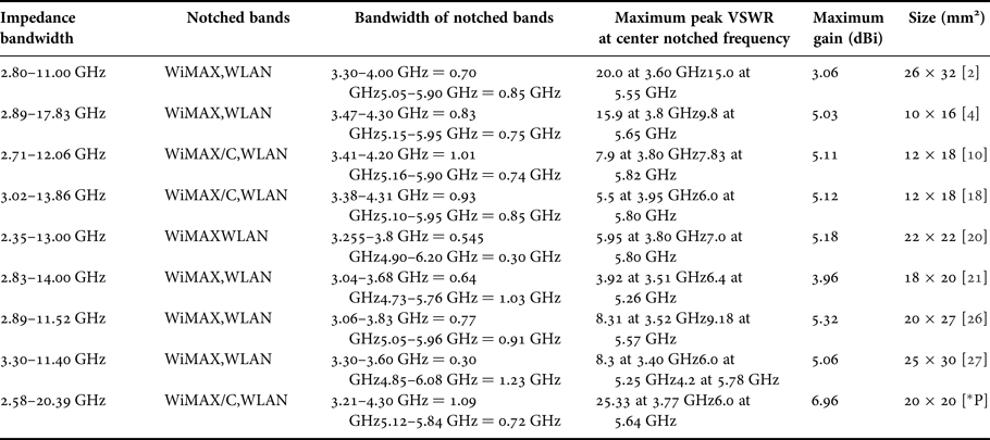
ω SR, ω PR are the series and parallel resonant frequencies and BW SR , BWPR are the corresponding bandwidth, which are noted from Figs 9(b) to 9(c) along with the values of R sn and R pn . Using the noted values, the value of L sn , Csn, Lpn , and C pn for equivalent circuit Fig. 8(b) are calculated by equations (5)–(8) where n = 1, 2, 3,…. Figure 8(c) represents snapshot of CST Design studio where equivalent circuit model is constructed using RLC components. Bandwidth and resonant frequencies are noted down from simulated impedance curve obtained from dual notched band UWB-extended band antenna from EM simulation. Considering UWB-extended band antenna as load impedance (Z La ), equivalent circuit model schematic is drawn in CST Design Studio. By optimizing the circuit element values, all the required passive components values are obtained and are tabulated in Table 2.
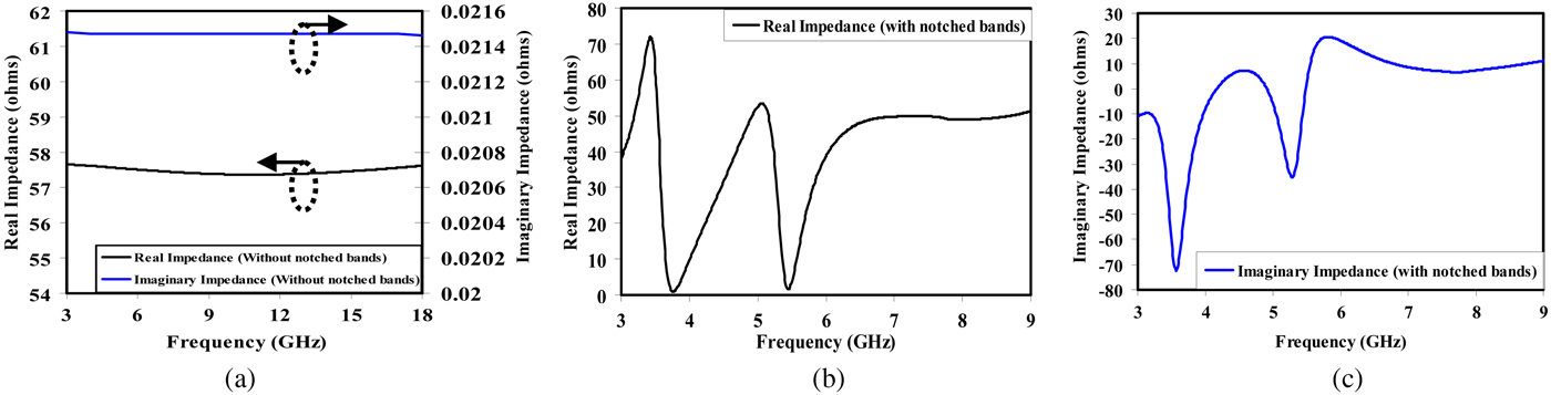
Fig. 9. Simulated input impedance of (a) UWB-extended bandwidth antenna, (b) real impedance of proposed antenna, (c) imaginary impedance of the proposed antenna.

Fig. 10. Proposed antenna (a) measured and simulated gain (dBi), (b) simulated radiation efficiency, (c) measured and simulated VSWR, (d) fabricated prototype.
Table 2. Optimized value of RLC components.

V. EXPERIMENTAL RESULTS
Measured gain of the proposed antenna and simple UWB-Ku band is shown in Fig. 10(a). A drop in peak gain is noted in notch band 13.80 at 3.45 GHz and 12.96 at 5.40 GHz, respectively. Effect of the two slots, which is responsible for notched bands for WiMAX/C and WLAN are analyzed. At the two notched bands the gain falls down below 0 dBi, which confirms that antenna does not radiate in these two notched bands, whereas gain is almost matched in the remaining UWB, X, and Ku bands without notched.
The antenna gain varies from 3.00 to 6.96 dBi. Simulated radiation efficiency is also shown in Fig. 10(b). Proposed antenna exhibits a good efficiency, being >80% across the entire radiating band except in two notched bands. Furthermore, the simulated radiation efficiencies of the proposed dual band-notched antenna, at 3.39 and 5.56 GHz, are only 12 and 16%, respectively. Figure 10(c) validates the proposed UWB antenna with dual notched bands. There is a slight disagreement between simulated and measured result due to reasons such as impedance match between SMA connector and microstrip soldered point. The measured rejection peaks have a VSWR 25.33 at 3.77 GHz, 5.64 at 6.0 GHz. Measured bandwidth for proposed antenna is 2.59–19.62 GHz.
Figure 11 depicts the measured radiating patterns, including the co-polarization and cross-polarization in the H-plane (x–z plane) and E-plane (y–z plane). It can be observed that nearly omni-directional radiation pattern with less co-polarization level can be seen in H-plane (x–z plane), which confirms its radiation characteristics in pass bands between 2.59 and 19.62 GHz. The main purpose of radiation pattern is to demonstrate that antenna actually radiates over a wide-frequency range. The radiation pattern in the E-plane (y–z) is small electric like dipole pattern and also, at higher frequencies cross-polarization increases to some extent because of increase in the area of radiation.

Fig. 11. Measured and simulated normalized radiation patterns in E- and H-planes (dB) at (a) 4.5 GHz, (b) 7.0 GHz, (c) 9.0 GHz, (d) 12.0 GHz, (e) 15.0 GHz, (f) 18.0 GHz.
Table 3 shows comparison of proposed antenna with published works at various parameters as impedance bandwidth, bandwidth of notched bands, maximum VSWR at center notched frequency, maximum gain and size. As observed, rejection at notched frequency (3.77 and 5.64 GHz) is high with maximum gain of 6.96 dBi. Also, with compact design, proposed antenna covers bandwidth of 17.81 GHz, which includes UWB, X, & Ku-band applications.
Table 3. Comparison of the proposed dual band-notched antenna parameters with several existing designs.

P* Proposed antenna.
VI. CONCLUSION
Compact dual band-notched 20 × 20 mm2 UWB-extended antenna was fabricated and tested, which is also capable for usage in multiple wireless services including close range radar (8–12 GHz) in X-band & satellite communication (12–18 GHz) in Ku band. Antenna demonstrates omni-directional radiation pattern in H-plane (x–z plane), which confirms its radiation characteristics in pass bands between 2.59 and 19.62 GHz and also antenna exhibits a good efficiency, being >90% across the entire pass band. Proposed monopole antenna exhibits salient properties for embedded multiple wireless transceivers for both indoor and outdoor applications. In addition, antenna is also useful for military requirement for land, airborne, novel radar, and fixed satellite service in X and Ku bands.
ACKNOWLEDGEMENTS
The authors are thankful to Krishna Ranjan Jha, Advance Microwave Antenna Testing Laboratory (URL: http://delhi.gov.in/wps/wcm/connect/doit_gbpec/GBPEC/Home/List+of+Labs), G. B. Pant Engineering College, Delhi for providing Antenna Measurement Facility.
 Manish Sharma received B.E. degree in Electronics and Communication Engineering from Mangalore University, Karnataka, India in 2000 and M.Tech. degree from Visvesvaraya Technological University, Karnataka, India in 2007. He has completed the Ph.D. degree from Banasthali University, Rajasthan, India from the Department of Electronics Engineering in 2017. His current research interest includes UWB antenna, RFID antennas, planar filters, phase shifters, metamaterial absorbers & cloaking, etc.
 Yogendra Kumar Awasthi (M'13) received the B.Sc. degree from Agra University, Agra, India in 1999, the M.Sc. degree from Agra University, Agra, India in 2001, in Electronics & Computational Physics and Ph.D. degree in RF & Microwave Engineering from Delhi University, Delhi, in 2012. He was visiting faculty at Central Electronics Engineering Research Institute, Pilani, and Rajasthan, India in 2012. He is currently working as Associate Professor with the Department of Electronics and Communication Engineering, Manav Rachna University, Faridabad, India. His research interest include Modeling high-frequency passive microwave components, Microwave antenna as 5G & Nano, Metamaterial absorber & cloaking, Study of transient, RF Power Transfer & Energy Harvesting, etc.
 Himanshu Singh received the B.Sc. degree from Agra University, Agra, India in 2000, the M.Sc. degree from Agra University, Agra, India in 2002, in Electronics & Computational Physics and Ph.D degree in RF & Microwave Engineering from Delhi University, Delhi, in 2010. She is currently working as Assistant Professor in Sri Aurobindo College, University of Delhi, New Delhi, India. Her research interest includes modeling & Simulation of MIC/MMIC components and UWB antenna, etc.