


Introduction
Impedance transformers or matching networks are important circuits in RF and microwave systems. In addition to providing good matching between two circuits, impedance transformers also affect the amplifier gain and noise figure of these systems. Impedance transformers consisting of transmission lines are commonly used because of the low cost and low parasitic effects owing to the absence of lumped elements or soldered connections.
As the demand for dual-band communication system increases, dual-band impedance transformers become more important. Dual-band impedance transformers using multi-section transmission lines have been developed to match a load with equal complex impedances [Reference Wu, Liu and Li1] and frequency-dependent complex impedances [Reference Liu, Liu, Li, Wu and Wu2]. Multi-section transmission lines with shunt stubs represent another configuration to match such loads [Reference Rawat and Ghannouchi3–Reference Liu, Zhang and Yang8]. Because shunt stubs can generate virtual ground, dual-band impedance transformers with a selectable transmission zero have been proposed to suppress unwanted out-of-band signals [Reference Chuang and Wu9, Reference Chuang and Wu10]. Dual-band impedance transformer using two parallel transmission lines has also been developed [Reference Wang, Ma and Ohira11].
Most of these studies have focused on concurrently achieving matching at the two operating frequencies. However, modern dual-band communication systems often operate at only one of these two frequencies. For instance, commercial WiFi equipment connects to an access point via either the 2.4 or 5.8 GHz band at an instant. Once an operating frequency is selected, the other one is often turned off to save power and avoid problems. The amplifier used in such cases generally combines two individual amplifiers with switches [Reference Candra and Xia12]. However, this topology requires a large circuit area and more components. Another way of implementing such an amplifier involves a single transistor with switchable input and output impedance transformers. One possible way uses switchable inductor and capacitor as an output matching network [Reference Ko, Lee and An13]. Another way of this type of switchable amplifier uses cascaded transmission lines and detachable shunt uniform stubs [Reference Fukuda, Okazaki, Hirota and Yamao14–Reference Norouzian16]. A switched band impedance transformer with a detached shunt stub and a fixed shunt stub has also been proposed [Reference Norouzian and Gardner17]. The common limitation in these works is that the characteristic impedances of the cascaded transmission lines must be 50 Ω, which restrict the design freedom and the circuit size is fixed. Further, these circuits provide good matching at the operating frequency, but do not guarantee total reflection at the non-operating frequency. Therefore, such systems may generate a large RF signal at the operating frequency and a non-negligible RF signal that is only slightly smaller at the non-operating frequency.
This work presents a switched-band impedance transformer composed of two cascaded transmission lines and two detachable shunt stepped-impedance open stubs with switching diodes to control the operating mode. With this transformer, the two aforementioned limitations of the previous works are resolved. The circuit parameters are obtained using the derived analytical design formula. Numerical simulations and experimental measurements are presented to validate the proposed structure and design formula.
Transformer structure and design formula
This work considers two operating frequencies, f 1 and f 2, which are arbitrary and uncorrelated. The frequency ratio is defined as α ≡ f 2/f 1. The load is considered to have a frequency-dependent complex impedance, i.e. the load impedances at the two operating frequencies are different. Figure 1 shows the structure of the proposed switched band impedance transformer. The electrical lengths of the transmission lines and stubs are measured at frequency f 1.
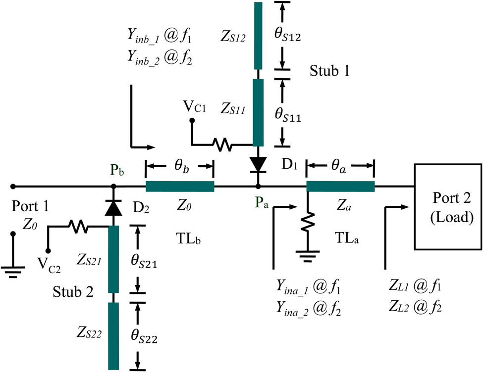
Fig. 1. The proposed switched band impedance transformer.
If transmission line TLa and stub 1 are used to match the lower frequency, f 1, the functions of the transmission lines and stubs as well as the design concept are described below. Transmission line TLa is used to obtain an input admittance $Y_{ina\_1}$ , seen by looking into the load and having the form $Y_0 + jB_{ina\_1}$
 at frequency f 1. If the load impedances at the two operating frequencies are Z L1 = R L1 + jX L1 at f 1 and Z L2 = R L2 + jX L2 at f 2, the electric length, θ a, of transmission line TLa can be determined as

where the characteristic impedance Za is a user-set parameter. Comparing with the previous study [Reference Norouzian and Gardner17], Za can be an arbitrary value instead of Z 0.
Once the input admittance is calculated, a shunt stub is added to cancel the input susceptance. When diode D 1 is forward biased and diode D 2 is reverse biased, stub 1 is connected to transmission line TLa at junction Pa and stub 2 is disconnected. Uniform-impedance stub14 can be used to cancel the input susceptance at f 1 but not guarantee to block the signal at f 2. In this study, stub 1, which has a stepped impedance, is used to cancel input susceptance Bina_ 1 at f 1 and generate a transmission zero (total reflection), to block the signal at f 2. Therefore, the lengths and the characteristic impedance of stub 1 must meet equations (2) and (3).


Solving these simultaneous equations for Z S11 and Z S12 yields


where the electrical lengths θ S11 and θ S12 are user-set parameters. Thus, the load impedance is transformed to Z 0 at f 1 and short-circuited at f 2.
To achieve matching at frequency f 2, diode D 1 is reverse biased and D 2 is forward biased. Thus, stub 1 is disconnected and stub 2 is connected to transmission line TLb at junction Pb. Transmission lines TLa and TLb are used to obtain the input admittance $Y_{inb\_2}$ , at junction Pb, seen by looking into the load and have the form $Y_0 + jB_{inb\_2}$
 at frequency f 2. The characteristic impedance of transmission line TLb is chosen as Z 0 so that it does not affect the matching condition at f 1.
The electrical length, θ b, of transmission line TLb at frequency f 1 can be determined as

where the input impedance at junction Pa without stub 1 is $R_{ina\_2} + jX_{ina\_2}$ at frequency f 2.
Once the input conductance is obtained, stub 2 is used to cancel input susceptance Binb_ 2 at f 2 and generate a virtual ground to block the signal at f 1. Therefore, the lengths and the characteristic impedance of stub 2 must satisfy equations (7) and (8) simultaneously.


Solving these equations for Z S21 and Z S22 yields


where the electrical lengths θ S21 and θ S22 are user-set parameters. Thus, the load impedance is transformed to Z 0 at f 2 and short-circuited at f 1. For convenience, the above solution is called Type 1.
The functions of the transmission lines and stubs can be interchanged with the same circuit structure. For convenience, this solution is called Type 2. Specifically, transmission line TLa and stub 1 in Type 1 are used to match the lower frequency, f 1, while transmission line TLa and stub 1 in Type 2 are used to match the higher frequency, f 2.
In Type 2, transmission line TLa is used to obtain an input admittance seen by looking into the load and having unit conductance at frequency f 2 while stub 1 is used to cancel the susceptance arising from transmission line TLa at frequency f 2 and to generate a transmission zero at frequency f 1 when diode D 1 is forward biased and diode D 2 is reverse biased. For matching at frequency f 1, diode D 1 is reverse biased and D 2 is forward biased. Thus, stub 1 is disconnected and stub 2 is connected to transmission line TLb. Transmission lines TLa and TLb are used to obtain a certain input admittance so as to have unit admittance at frequency f 1. Stub 2 is used to cancel the susceptance arising from transmission lines TLa and TLb at frequency f 1 and to generate a transmission zero (total reflection), at frequency f 2. In this case, the design formula is modified as equations (11)–(16).


and


In these equations, Bina_ 2 denotes the input susceptance at frequency f 2 at junction Pa, $R_{ina\_1} + jX_{ina\_1}$ denotes the input impedance at frequency f 1 at junction Pa without stub 1, and Binb_ 1 denotes the input susceptance at frequency f 1 at junction Pb.
Design example
To verify the proposed structure and design procedure, a switched band impedance transformer using microstrips was designed, fabricated, and measured. The arbitrary two operating frequencies used were 0.9 and 2.1 GHz. The transformer was designed and fabricated on a 1.6 mm-thick FR4 substrate with a dielectric constant of 4.35 and a loss tangent of 0.016. The load used was a 100 Ω resistor and an SMA connector shunt connected with a 1 pF capacitor. The corresponding load impedances were 87.24-j74.00 and 30.50-j60.38 Ω at the two operating frequencies, respectively.
Figure 2 shows the variation of the required electrical length θa versus the characteristic impedance Za of transmission line TLa for Type 1. In this case, the length θa decreases as the impedance Za increases. Because Za is a user-set parameter, the designer can choose a suitable value to minimize θa under PCB fabrication constrains, such as width limitations. In contrast, traditional single-frequency matching networks or previous switched matching networks14 often use a 50 Ω transmission line, such that the circuit size is fixed and cannot be reduced. For example, the required length θa is about 60° if Za was chosen as 100 Ω which is a typical upper value of general PCB technique. While if Za was chosen to be equal to the traditional value of 50 Ω, the required length θa would be more than 100°. The proposed structure can reduce the required length by 60%. In this example, Za was chosen as 75 Ω and the required θa was 82.80° at 0.9 GHz.

Fig. 2. Variation of the required electrical length θa (at 0.9 GHz) versus the characteristic impedance Za of transmission line TLa for Type 1.
As to transmission line TLb, there were two solutions that could be chosen. In this example, θb was chosen as 29.32° at 0.9 GHz. Figure 3(a) demonstrates the variations of the required ZS 11 and ZS 12 versus θS 12 for different values of θS 11. Because θS 12 and θS 11 are user-set parameters, suitable values can be chosen to obtain reasonable stub impedances, i.e. neither extremely high nor extremely low. For example, ZS 11 and ZS 12 are between 25 and 100 Ω when θS 11 = 10° and 13° < θS 12 < 35°. Figure 3(b) shows a similar phenomenon for stub 2.
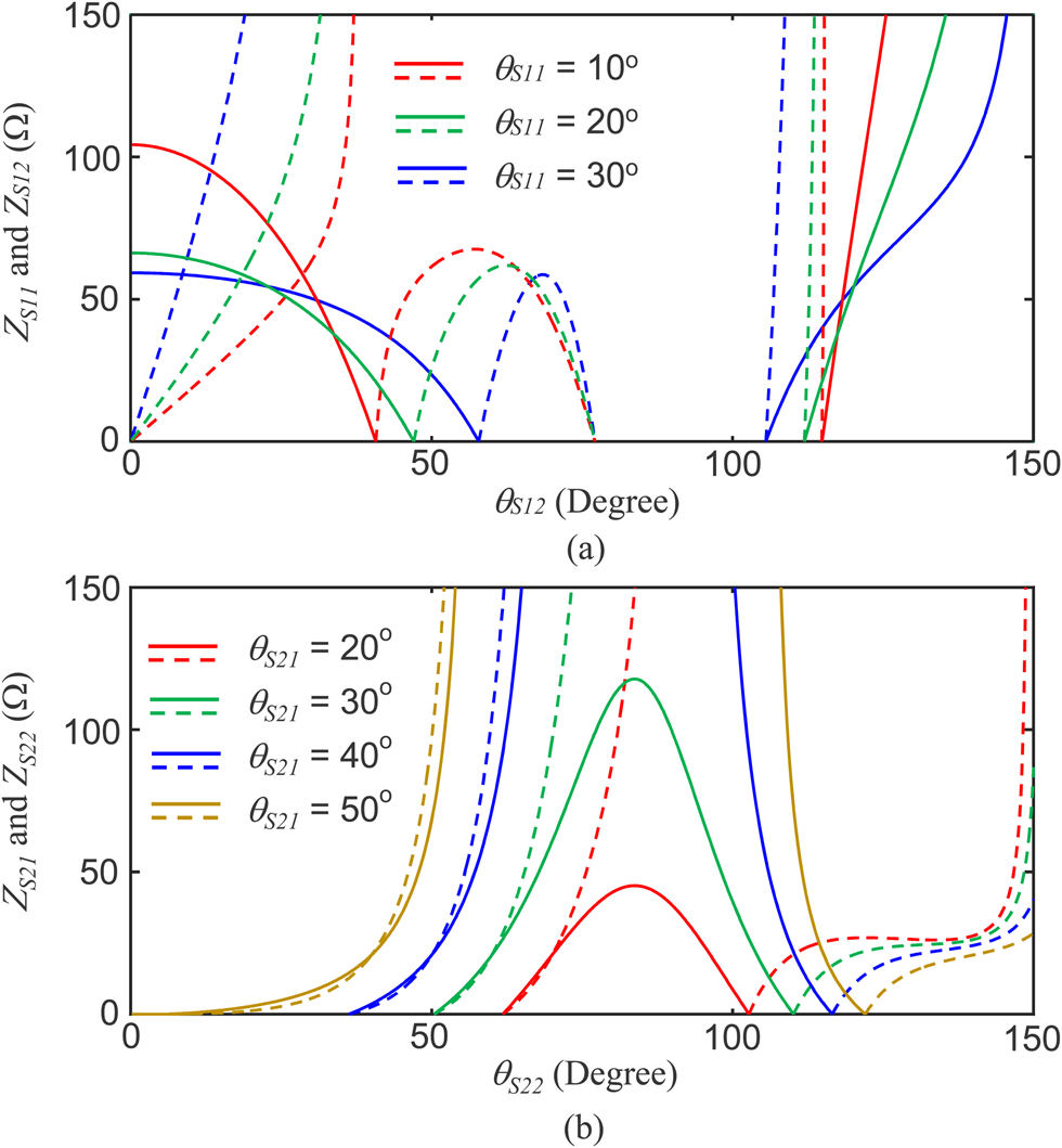
Fig. 3. Variation of the required stub impedances versus stub lengths, (a) ZS 11 (solid line) and ZS 12 (dashed line) against θS 12 for different θS 11, (b) ZS 21 (solid line) and ZS 22 (dashed line) against θS 22 for different θS 21.
For Type 2, Fig. 4 demonstrates the variation of the required electrical length θa versus the characteristic impedance Za of transmission line TLa. Figure 4 shows that a higher impedance transmission line requires a shorter length. As Type 1, the designer can choose a suitable value to minimize θa under PCB fabrication constrain, such as width limitations. Here Za was chosen to be 75 Ω as Type 1 and thus the required length θa was 26.09° at 0.9 GHz. In contrast, the switched matching network that uses a 50 Ω transmission line requires θa of more than 34°. The choice of the characteristic impedances and lengths of stubs 1 and 2 is similar to Type 1.

Fig. 4. Variation of the required electrical length θa (at 0.9 GHz) versus the characteristic impedance Za of transmission line TLa for Type 2.
Table 1 lists the parameters of the two designed circuits, where the underlined values denote user-set parameters and the rest were obtained using the proposed design formula. Figure 5 shows the frequency responses of the two designed switchable transformers which were simulated using Ansoft Designer (now called ANSYS HFSS-Circuit) with ideal transmission line model. The diodes were considered as ideal in our numerical simulation, i.e. open when zero-biased and shorted when forward-biased. In the lower-band mode, diode D 1 is forward-biased and diode D 2 is zero-biased. In this mode, the frequency response showed a good matching exactly at the operating frequency, 0.9 GHz, and a reflection of 0 dB at the non-operating frequency, 2.1 GHz. In the higher-band mode, diode D 1 is zero-biased and diode D 2 is forward-biased. The frequency response showed a good matching exactly at 2.1 GHz and a reflection of 0 dB at 0.9 GHz. Due to the restriction of total reflection at the non-operating frequency, the matching bandwidth of the presented impedance transformer is narrower than the traditional single-band impedance transformer which does not concern with total reflection at other frequencies.

Fig. 5. Simulated reflection coefficients of the two designed switch-band impedance transformers with different diode biasing conditions.
Table 1. Circuit parameters of the designed switched band impedance transformers where parameters with underline are user-setting.

The electrical lengths are measured at 0.9 GHz.
Figure 6 compares the numerical results of Type 1 using stepped-impedance stubs and traditional structure using uniform-impedance stubs. If the matching frequency is 2.1 GHz, the structure using stepped-impedance has S 11 of 0 dB at 0.9 GHz while the structure using uniform-impedance stub has S 11 of −12 dB. It is clear that the circuit using stepped-impedance stub can suppress signal at the non-operating frequency and the one using uniform-impedance stub has no such function.

Fig. 6. Comparison between impedance transformers with uniform-impedance stubs and stepped-impedance stubs.
Figure 7 shows a comparison of the numerical and measured frequency responses where the fabricated transformer Type 1 is embedded. This work used Infineon BAR63-02V PIN diodes. The experimental results were obtained using an R&S ZVA40 network analyzer. In the lower-band mode, the simulation revealed a good match at 0.9 GHz and total reflection (0 dB) at 2.1 GHz. The measurements showed good matching at 0.9 GHz and a reflection of −2.4 dB at 2.1 GHz. The bandwidths of the simulations and measurement are 338 and 383 MHz, respectively. In the higher-band mode, the simulation revealed a good match at 2.1 GHz and total reflection at 0.9 GHz. The bandwidths of the simulations and measurement are 98 and 113 MHz, respectively. The measurements showed a good match at 2.1 GHz and a reflection of −1.4 dB at 0.9 GHz. The deviations between the simulated and measured results may be due to fabrication errors, discontinuity effects, substrate losses, and non-ideal diodes. These factors were not considered in the design formula and simulation. The non-zero forward resistance of the PIN diode in the ON state, which degrades the virtual ground at junctions Pa and Pb, can be improved by replacing the PIN diode with an MEM switch, which has a very low insertion loss in the ON state, may improve the measured reflection at the non-operating frequency.
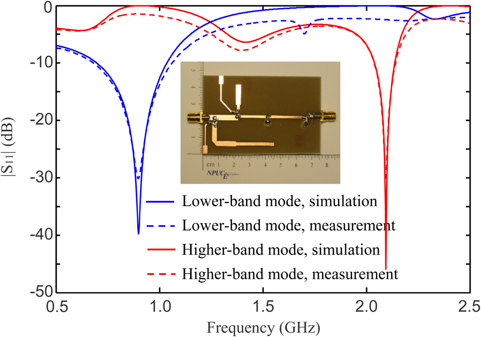
Fig. 7. Simulated and measured reflection coefficients of the fabricated switched band impedance transformer with different diode biasing conditions.
Table 2 compares this work and published researches about switched-band impedance transformers.
Table 2. Comparison between this work and other researches

Conclusion
This work presents a switched-band matching network that can match a frequency-dependent complex impedance load at one of the two uncorrelated frequencies. The characteristic impedance of the transmission line connected to the load can be arbitrary instead of the traditional Z 0, which can potentially reduce the size of the circuit. The detachable stepped-impedance shunt stubs ensure good matching at one of the two frequencies and a virtual ground that suppresses the signal at the non-operating frequency. The derived analytical formula simplifies the design process and does not involve time-consuming iterative procedures. The numerical simulations and experimental measurements validated the proposed structure and design formula. The presented structure can thus be applied to switched-band amplifier and mixer designs.
 Ming-Lin Chuang received the B.S. degree in electrical engineering from National Central University, Taoyuan, Taiwan, in 1991, M.S. and Ph.D. degrees in electrical engineering from Tatung Institute of Technology, Taipei, Taiwan, in 1993 and 1998, respectively. In 2000, he joined the faculty of the Department of Communication Engineering, National Penghu University of Science and Technology, Penghu, Taiwan, and as the chair from 2000 to 2005 and 2010 to 2016. He is currently the Professor of the department. Dr. Chuang's research interests include RF/microwave passive and active circuits, antennas, and Internet of things.
 Ming-Tien Wu received the B.S. and Ph.D. degrees in electrical engineering from Tatung Institute of Technology, Taipei, Taiwan, in 1988 and 1996, respectively. In 1998, he joined the faculty of the Department of Communication Engineering, National Penghu University of Science and Technology, Penghu, Taiwan. He is currently the Associate Professor and Chair of the department. Dr. Wu's areas of research include microwave passive circuits and antennas.
 Shu-Min Tsai received the B.S. degree from the National Taiwan Ocean University, Keelung, Taiwan, in 1992, and the M.S. degree in 1994, respectively, and the Ph.D. degree from the National Cheng Kung University, Tainan, Taiwan, in 2007, all in Electrical Engineering department. She is now an Associate Professor in the Department of Communication Engineering of National Penghu University of Science and Technology, Penghu, Taiwan. Dr. Tsai's research interests include communication circuit and system, Internet of things, and signal processing.


