


Introduction
The fifth-generation (5G) mobile communication is going to be in service worldwide in coming years [1]. It has the characteristic of wide bandwidth, high data rate, and low latency to satisfy 5G EMBB, IoT, and URLLC application scenarios. In sub-6 GHz band, the 3GPP Release 15 has designated operation frequency bands for 5G New Radio Access Technology, as illustrated in Table 1.
Table 1. The 5G new radio access technology band [1]

In the competition of European Microwave Week (EuMW) 2019, the design specifications and rules were defined as
• Passband 1: 900 to 1000 MHz.
• Passband 2: 1427 to 1518 MHz.
• Passive designs only.
• Acoustic-wave-based filters are not allowed.
• The implemented filter should be suitable for visual inspection, and sealed casing is not allowed.
The specified passband frequency ranges cover six 5G NR bands, i.e. n8, n50, n51, n74, n75, and n76. A figure of merit (FoM) is defined as below to evaluate the overall performance:

In (1), A is the circuit size in mm2 and |S 21(f)| indicates the absolute value of measured S 21 in dB at the frequency f in MHz, where four passband edge frequencies are calculated, namely, fP 1 = 900 MHz, fP 2 = 1000 MHz, fP 3 = 1427 MHz, and fP 4 = 1518 MHz, and three stopband frequencies are included, including fS 1 = 850 MHz, fS2 = 1050–1350 MHz, and fS3 = 1600 MHz.
To satisfy the two-passband requirement, the dual-band bandpass filter (BPF) must be employed. The dual-band filter was first introduced in [Reference Makimoto and Yamashita2, Reference Sagawa, Makimoto and Yamashita3], where the stepped-impedance resonator (SIR) was proposed to generate two resonance frequencies with arbitrary ratio by choosing a proper impedance ratio. In other words, the center frequency of the second passband does not need to be the harmonic of the first passband (f 2≠2 × f 1).
On the other hand, for the improvement of bandwidth, selectivity, and stopband rejection in a dual-band filter, the arrangement of the SIRs was found playing an important role in the inter-band and out-of-band suppression, which includes the hairpin, comb, interlock configurations [Reference Chang, Jeng and Chen4–Reference Tang and Wu6]. Moreover, since the coupling coefficient between SIRs controls the passband bandwidth, three different coupling structures are presented in [Reference Lee, Chen, Tsai and Tsai7] to provide flexibility on the design of coupling coefficient. In [Reference Kuo and Lin8], the stopband of SIR filter is extended by the relocated transmission zeros. By adjusting the coupling length and tap position of input and output resonators, the zeros are moved to the desired frequencies to suppress the harmonic spurious. In [Reference Tang and Wu6], another novel coupling structure of SIRs is proposed. With the use of mutual coupling on both ends of resonators, the transmission zeros show up to enhance selectivity. In addition, for the enhancement of second passband, a novel SIR with asymmetric line subresonator is introduced in [Reference Hsu, Chen and Chuang9].
Therefore, to achieve the best FoM, the interlocked SIR configuration [Reference Tang and Wu6] is adopted in this design. Although the interlock configuration provides the better insertion and stopband suppression, it has a drawback of larger empty layout space. This drawback will be resolved by folding the SIRs. Also a capacitive loading at the SIR is incorporated to further enhance the upper stopband suppression.
Circuit design
The proposed filter, as shown in Fig. 1(a), consists of two interlocked SIRs, where the SIR is composed of three equip-length transmission line sections. Compared to the conventional configuration, where the coupling only takes place on one section of the SIR, the both end-sections of the first SIR are coupled to those of the second SIR. This interlocked coupling configuration not only lowers the passband insertion loss but also introduces three extra transmission zero, considerably enhancing to stopband suppression.

Fig. 1. Schematic diagrams of the dual-band BPF, (a) the proposed interlocked configuration, (b) the parallel coupled configuration.
Stepped-impedance resonator
From the SIR theory [Reference Makimoto and Yamashita2], two simultaneous passbands are corresponding to the first two lowest resonance modes of the SIR. Hence, the resonance condition of the interlocked SIR is investigated first. For simplicity, the shift of the resonance frequencies induced by the coupling of the interlocked segments is ignored. The SIR is composed of three equal-length line sections (θo), where both end-sections have the same characteristic impedance Z 1 and the central section has Z 2. The total electric length of the SIR is 3θo and the characteristic impedance ratio is designated as r = Z 2/Z 1.
Since the SIR is symmetric to the reference plane P, the resonance modes can be conveniently categorized into the odd and even modes. For the odd mode, the reference plane P is regarded as the short circuited to the ground and it is taken as the open circuited for the even mode. The resonance equations were derived by [Reference Makimoto and Yamashita2] as


From (2), there are consecutive odd resonance modes with discrete resonance frequencies and similarly for the even mode. By arranging the resonance frequency in increasing order, the first passband at fo 1 comes from the first odd mode and the second passband at fo 2 is corresponding to the first even mode. Therefore, the passband frequency ratio can be obtained as

As indicated in (4), the ratio of passband frequencies can be controlled by the impedance ratio r of the SIR. Figure 2 shows the calculated frequency ratio and the electric length θo,odd at fo 1 with respect to the impedance ratio r. If the impedance ratio r is larger than 1, the passband frequency ratio lies between 1 and 2. On the other hand, if the impedance ratio r is smaller than 1, the passband frequency ratio becomes larger than 2. In Fig. 3, the frequency response demonstrates the flexible design of the second passband. By fixing the first passband of 900–1000 MHz, the second passband is located at 1840–1940, 1423–1523, and 1261–1361 MHz corresponding to the impedance ratio r of 1.01, 2.01, and 3.01, respectively. For the case of this work, the required passbands are 900–1000 MHz and 1427–1518 MHz, giving the frequency ratio of 1.55. The impedance ratio must be 2.01, and the electric length θo is 70.6° at 950 MHz.

Fig. 2. The frequency ratio of the first two passbands with respect to the impedance ratio r of the SIR.

Fig. 3. The frequency response of SIRs with the impedance ratio of 2.01, 3.01, and 4.01, respectively.
Since the required passband frequencies determine the impedance ratio of SIRs only, the impedance of SIRs must be completely determined by the required bandwidth. With the same impedance ratio of 2.01, Fig. 4 demonstrates the adjustable bandwidth with respect to the impedance Z 1 = 15, 35, 55 Ω, and Z 2 = 30.15, 70.35, 110.55 Ω, respectively. In this work, by considering the stop rejection at fS 1 = 850 MHz, fS 2 = 1050–1350 MHz, and fS 3 = 1600 MHz, the impedance is selected as Z 1 = 55 Ω and Z 2 = 110.55 Ω.

Fig. 4. The bandwidth variation of the first two passbands with different Z 1 and Z 2.
Transmission zeros of interlocked SIRs
A remarkable advantage of the interlocked SIRs is the introduction of three transmission zeros by the coupled section of the SIR [Reference Tang and Wu6], which were derived as

In (5), k denotes the coupling coefficient of the coupled section. Therefore, by carefully designing the coupling coefficient k and the impedance ratio r to satisfy the condition fo 1 < fz 2 < fo 2, the inter-band suppression can be considerably enhanced by the second transmission zero (fz 2). The lower stopband and upper stopband suppression can be enhanced by the first transmission zero (fz 1) due to fz 1 < fo 1 and by the third transmission zero (fz 3) due to fo 2 < fz 3.
Simulation and measurement results
As discussed in the section ‘circuit design’, the impedance ratio r = 2.01 and the electrical length θo = 70.6° of the SIR are used to generate two passbands at 900–1000 and 1427–1518 MHz. There is a degree of freedom to choose the characteristic impedance Z 1. Here we choose Z 1 = 55 Ω and then Z 2 is 110.5 Ω. For the coupling section, Ze = 150 Ω and Zo = 110 Ω are determined by k = 0.15.
The substrate RO4003C was used for circuit implementation, which has a relative dielectric constant of 3.55, loss tangent of 0.0027, and the thickness of 0.5 mm. To minimize the circuit size, the center section of the SIR is folded to have the best space utilization, as shown in Fig. 5.

Fig. 5. The layout of the designed filter, (a) unfolded, (b) folded.
It is worthwhile to note that an open stub is added to the folded section. The open stub increases the capacitance to adjust Zin 2 of the SIR, then the frequency of the third transmission zero fz3 can be shifted.
The simulated insertion losses of the folded circuit with different open-stub lengths are presented in Fig. 6. Two passbands are correctly generated at the required frequency ranges and three transmission zeros are generated at the lower stopband, inter-passband, and upper stopband, respectively. Particularly, the transmission zero at the upper stopband is tunable by the open-stub length.

Fig. 6 Simulated results of the designed dual-band BPF. Note that the transmission zero at the upper stopband can be tuned.
The simulated 3 dB bandwidth for two passband are 889–1011 and 1389–1558 MHz, respectively, equivalent to the fractional bandwidth of 12.5 and 11.1%, respectively.
The photograph of the implemented circuit is shown in Fig. 7. The circuit size, excluded SMA connectors, is 41.40 mm × 19.96 mm, corresponding to $0.25 \times 0.12\,\lambda _g^2$ . Compared to the unfolded layout, the size reduction factor is 46%.
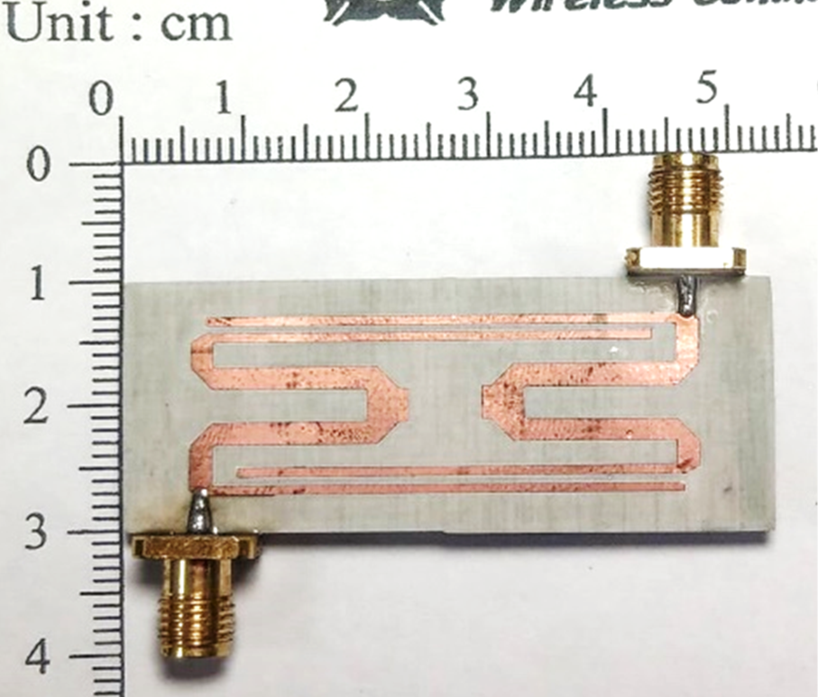
Fig. 7. The photograph of designed dual-band BPF with two interlocked SIRs.
The measurement results are shown in Fig. 8, where the simulation results are also plotted. The measured return loss is greater than 10 dB over the first passband (900–993 MHz) and the second passband (1409–1549 MHz). The measured insertion losses at the band edges are 1.61, 2.16, 1.15, and 1.26 dB, respectively. The frequencies of transmission zeros are at 750, 1189, and 1669 MHz, which give at least 38 dB suppression at those frequencies. For the desired stopband ranges, the stopband suppression are 11.53 dB in the lower stopband (500–850 MHz), 7.07 dB at the inter-passband (1050–1350 MHz), and 11.37 dB at the upper stopband (1600–2000 MHz).
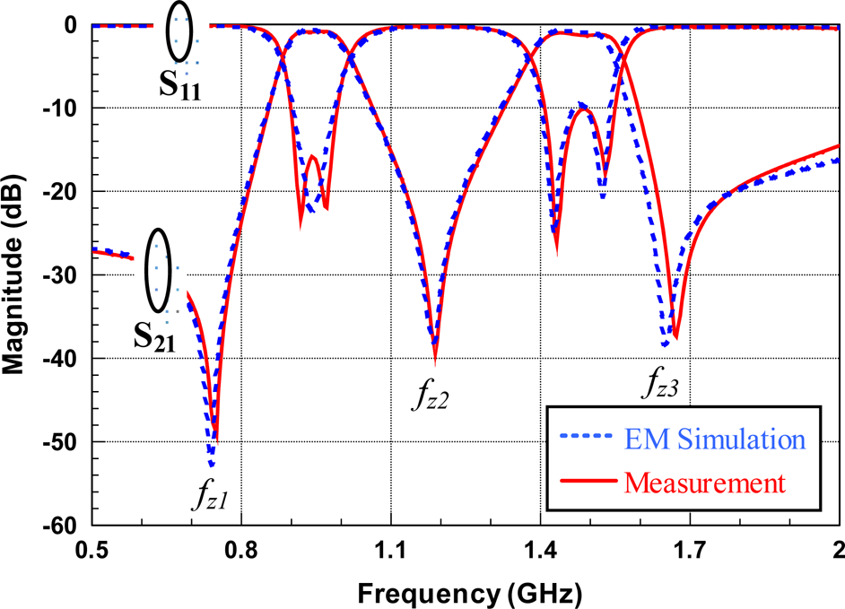
Fig. 8. The measured insertion and return losses of the implemented dual-band BPF with two interlocked SIRs.
The performance of this work and the dual-band BPFs reported in literature are listed in Table 2. Among these filters, the bandwidth at two passbands may have large difference except that our work has the best balance of bandwidth.
Table 2. Performance comparison of our work and reported dual-band SIR filters

Conclusion
The design of a compact dual-band BPF for the EuMW 2019 Student Design Competition is presented. Two passband are specified at 889–1011 and 1389–1558 MHz, which cover six 5G NR bands, i.e. n8, n50, n51, n74, n75, and n76. To achieve the best FoM defined by the competition committee, an interlock configuration of two centrally-loaded SIRs is employed, which has three benefits. First, the impedance ratio of the folded SIR can be designed to have two passbands with arbitrary frequency ratio. Second, the coupling section of the SIR generates three distinct transmission zeros, which are distributed at the lower stopband, inter-passband, and the upper stopband, respectively. The third benefit is the open stub loaded at the center of the SIR can be used to tune the upper transmission zero frequency.
The measured passband insertion losses are smaller than 2.16 dB at both passbands (900–1000 and 1427–1518 MHz). The stopband suppression at three transmission zeros are greater than 38 dB. The circuit size is as compact as 41.40 × 19.96 mm2, equivalent to $0.25 \times 0.12\,\lambda _g^2$ . The measurement results demonstrate strong potential for this dual-band BPF in the applications for sub-6 GHz 5G New Radio Access Technology. The proposed SIR can be extended to more than two passbands by modifying the proposed two-sectional stepped-impedance structure. For example, for the case of a triple-band BPF, the tri-sectional SIR with three different impedances and lengths can be used.
Acknowledgement
This work was partially supported by the MOST, Taiwan under project number MOST108-2218-E-194-005.
 Wei-Lun Hsu received the Bachelor's degree in electrical engineering from National University of Tainan (NUTN), Tainan, Taiwan, in 2019. Since 2019, he has been pursuing the Master's degree at National Chung Cheng University (CCU), Chiayi, Taiwan. His research interests include millimeter-wave switches and array antennas.
 Pei-Yu Lyu received the B.S. degree in electrical engineering from National University of Kaohsiung, Taiwan, in 2012, and the M.S. degree in electrical engineering from National Chung Cheng University, Taiwan, in 2015. She is currently working toward the Ph.D. degree at National Chung Cheng University, Taiwan. Her research interests include the integration and application of millimeter-wave radar system.
 Sheng-Fuh Chang received the B.S. and M.S. degree in communication engineering from National Chiao-Tung University, Taiwan, in 1982 and 1984, respectively, and the Ph.D. degree in electrical engineering from the University of Wisconsin at Madison in 1991. In 1994, he joined the Department of Electrical Engineering, National Chung Cheng University, Taiwan, where he is currently a Full Professor with the Department of Electrical Engineering and the Department of Communications Engineering, and the Director of the Center for Telecommunication Research. His research interests include micro-power electromagnetic vital signal detection, wireless indoor locating techniques, multiantenna beamforming systems, microwave/millimeter-wave monolithic integrated circuits for broadband wireless RF transceivers, and the design and test for the fifth generation (5G) mobile communication system.


