Introduction
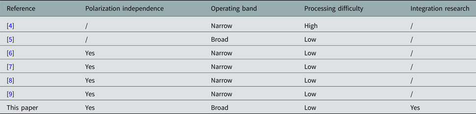
With the improvement of precision and sensitivity, electronic devices are seriously threatened by high-intensity radiation field (HIRF) and electromagnetic pulse (EMP). It is necessary to take measures to protect the electronic devices from being destroyed by high-power radiation in complex electromagnetic environment, e.g. using radiation shields or limiter circuit. In recent years, adaptive protection methods have attracted a lot of attention because they can change working state with the intensity of incident wave – for instance, switching non-linear metamaterial [Reference Wall, Rudolph, Hong and MorganWall1], non-linear power-dependent impedance surface [Reference Luo, Chen, Long and Quarfoth2], and limiting frequency-selective surface (FSS) [Reference Monni, Bekers and Wanum3]. Self-actuated frequency-selective surface (SFSS), an energy-aware protection method, offers superior regulatory characteristic compared with other approaches. Some FSSs utilized the semiconductor-to-metal phase transition of vanadium dioxide to achieve limiting property [Reference Scott, Nordquist, Cich, Jordan and Rodenbeck4]. An FSS consisted of PIN diodes and metal grid was designed for the limiting of linear polarized wave [Reference Yang, Liu and Huang5]. To realize polarization independence, several symmetric FSSs were reported [Reference Deng6–Reference Chen, Chen and Xu9]. The comparison of different self-actuated FSSs is shown in Table 1. As we can see, there are many limitations in most of SFSSs mentioned above, such as the difficulty of assemble technology, the narrow operating band, and polarization sensitivity. The proposed SFSS not only overcomes the weakness but also has little effects to the performance of antenna. It exhibits great potentials in electromagnetic compatibility and electromagnetic protection.
Table 1. Comparison of different self-actuated FSSs

The proposed SFSS, consisting of PIN diodes and metallic patches, spontaneously adjusts the characteristic impedance in accordance with the intensity of the incident wave. Signals below the safety threshold keep the state of diodes unchanged so that the surface maintains high equivalent impedance. Therefore, most of the energy of incident wave passes through the SFSS with little attenuation. On the contrary, when the induced voltage induced by incident wave exceeds the breakover threshold of the diodes, the equivalent impedance decreases rapidly so that the SFSS switches from transparent to reflection. As a result, the electronic devices can avoid irreversible damage caused by HIRF/EMP with the protection of the SFSS.
The SFSS is analyzed by the equivalent circuit method, which is widely used in the design of periodic structures, such as left-hand material [Reference Chen, Ran, Huangfu and Grzegorczyk10], FSS [Reference Costa and Monorchio11], and perfect metamaterial absorber [Reference Pang, Cheng, Zhou and Wang12]. Moreover, the surface current distributions of the SFSS give a better understanding to its physical mechanism.
This paper is organized as follows: in “Submission design and simulation of the radome” section, a SFSS radome suitable for any polarized wave is designed and simulated by Computer Simulation Technology Microwave Studio (CST MWS), besides, the equivalent circuit and surface current of the SFSS are presented and analyzed. In “Prototype fabrication and measurement” section, the prototype of the SFSS radome is fabricated to obtain the transmission characteristics, which are compared with the simulation results. Then, the non-linear response of the SFSS is verified in the rectangular waveguide; besides, a microstrip antenna integrated with the radome is designed and measured. Conclusions are drawn in “Conclusion” section.
Submission design and simulation of the radome
Structure of SFSS
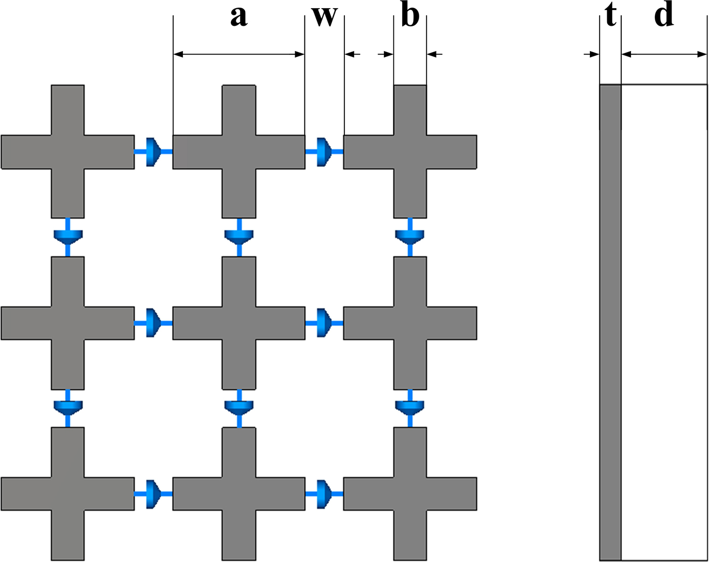
An ideal self-actuated FSS should effectively reflect the HIRF/EMP, while allow the normal signal to pass through it with little insertion loss. Figure 1 illustrates the structure of SFSS, which is composed of metallic crosses and PIN diodes arranged periodically above a dielectric substrate of Teflon (ε r = 2.1). The optimized dimensions of the unit cell are shown in Table 2. The symmetrical structure ensures that the SFSS maintains stable performance under different polarizations. Besides, the periodicity of SFSS is much less than the minimum operating wavelength so that the grating lobes can be avoided.

Fig. 1. Structure of the SFSS. (a) Front view, (b) side view.
Table 2. Dimensions of the SFSS radome

Equivalent circuit model of PIN diode
The self-triggered switchable function is based on the voltage-controlled characteristic of diodes [Reference Yang, Liu and Huang5]. Therefore, the performance of FSS is greatly influenced by diodes. Based on the method given in the product data sheet, the sample of diode BAP 51-02 is inserted in series with 50 Ω microstrip line to obtain the S parameters. As shown in Fig. 2(a), both ports of the sample are connected to the Keysight vector network analyzer PNA-X so that signals are captured after passing through the diode. After calibration, the transmission characteristic of the diode is measured in OFF state. To get the S parameters in ON state, there is a pair of bias tees coupled to the sample. As depicted in Fig. 2(b), the bias voltage passes through the DC ports, while the signal of vector network analyzer flows through the RF ports, thus conducting the diode in isolation of the DC and RF. According to the data sheet of BAP 51-02, the typical value of forward voltage is 0.95 V, so the bias added at the end of diode reaches 1 V.
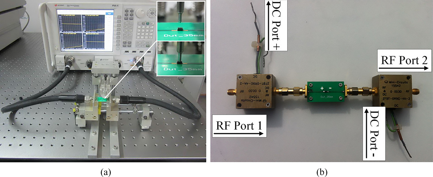
Fig. 2. Photograph of S parameters measurement of BAP 51-02. (a) OFF state, (b) ON state.
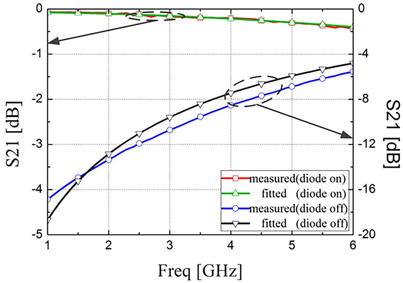
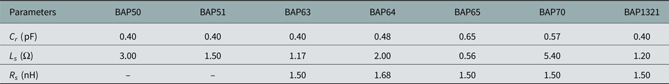
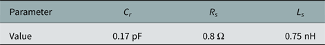
The product data sheet of BAP series diodes provides the typical values of main circuit parameters of different diodes, which is given in Table 3. The junction capacitance C r is measured in 1 MHz with 0 V, while the forward resistance R s and the lead inductance L s are measured in 100 MHz with 10 mA and 100 MA, respectively. Obviously, the measurement condition and frequency for main circuit parameters are quite different from the operating frequency range of the SFSS. In order to better describe the transmission characteristics of the diode, the S parameters are measured over 1–6 GHz. The equivalent circuits of diodes for different states are based on the electrical characteristic given in the product data sheet, an approximate capacitance C r at zero bias while a resistance R s in series with an inductance L s in the forward-biased state. The typical value of parameters, fitted by the Advanced Design System (ADS), is shown in Table 4. As depicted in Fig. 3, the S parameter of equivalent circuit agrees well with that measured by vector network analyzer, confirming the validity of the circuit model.

Fig. 3. S parameters of BAP 51-02.
Table 3. The steady-state circuit parameters of BAP series diodes

Table 4. Equivalent circuit parameters of BAP 51-02

Equivalent circuit models of SFSS
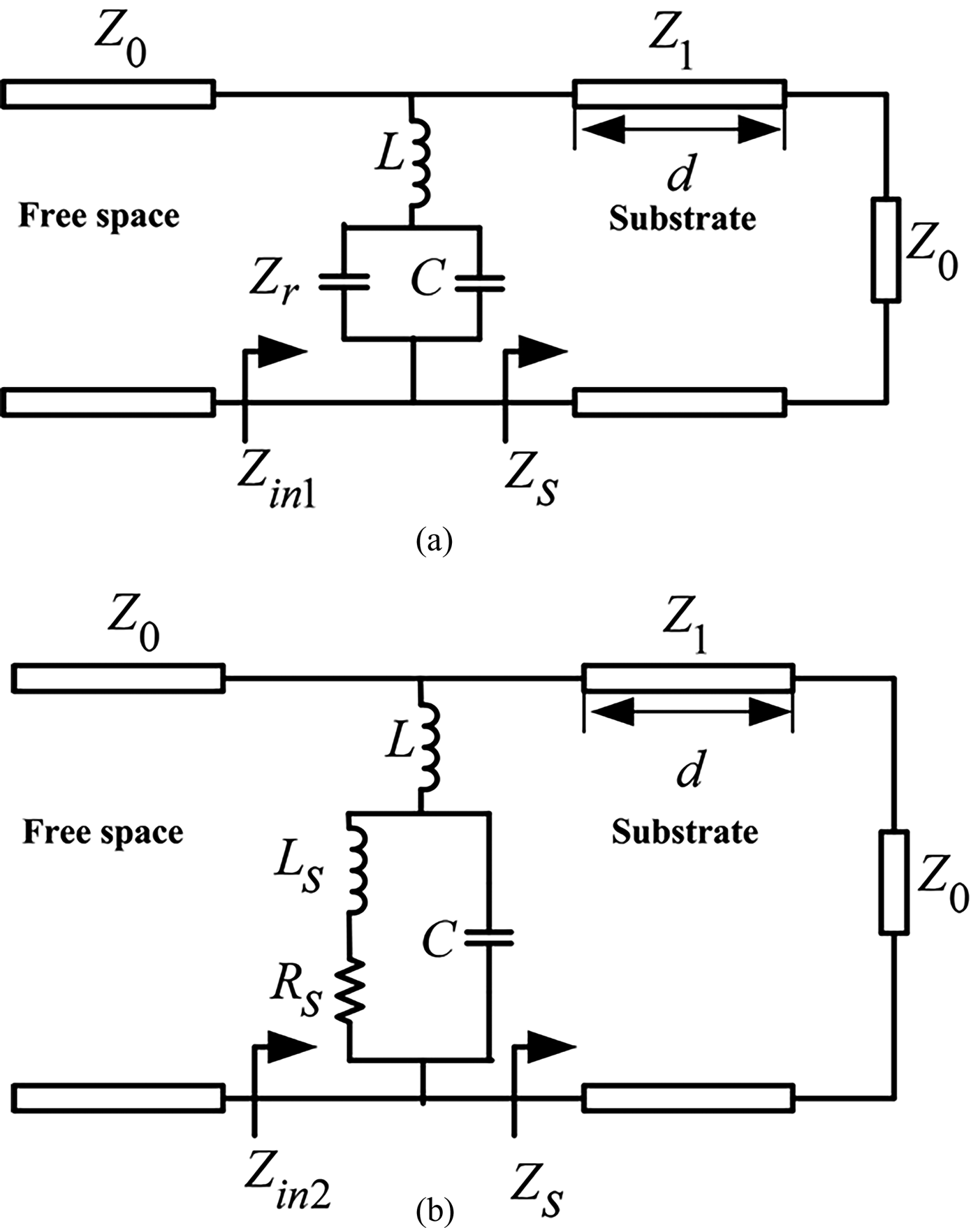
In the process of design, an equivalent circuit of the structure is established to analyze the performance of the SFSS. Based on the equivalent circuit method [Reference Costa and Monorchio11, Reference Roberts, Ford and Rigelsford13], the metallic crosses can be represented by a parallel LC circuit, and the diodes inserted in the gap of units can be modeled to be a parallel equivalent circuit. The equivalent circuit for both normal and oblique incidences is shown in Fig. 4. As we can see, L, C, and C r can form a wide passband in low frequency; however, the transmission window is removed when R s in series with L s substitutes C r. Therefore, the frequency responses of the SFSS are obtained through the simulation of equivalent circuit model once L and C are determined.

Fig. 4. Equivalent circuit model of the SFSS. (a) Diodes off, (b) diodes on.
For normal incidence, the equivalent capacitance C is calculated as following [Reference Marcuvitz14]:
 $$\displaystyle{B \over {Y_0}} = \displaystyle{{4\left( {a + w} \right)} \over \lambda} \left\{ \matrix{\ln \csc \displaystyle{{\pi w} \over {2\left( {a + w} \right)}} \hfill \cr + \displaystyle{1 \over 2}\displaystyle{{(1 - \beta _C^2 )^2 [2A_c (1 - \displaystyle{{\beta _C^2} \over 4}) + 4\beta _C^2 A_C^2 ]} \over {(1 - \displaystyle{{\beta _C^2} \over 4}) + 2A_c \beta _C^2 (1 + \displaystyle{{\beta _C^2} \over 2} - \displaystyle{{\beta _C^4} \over 8}) + 2\beta _C^2 A_C^6}} \hfill} \right\},$$
 $$A_C = \displaystyle{1 \over {\sqrt {1 - \left( {\displaystyle{{a + w} \over \lambda}} \right)^2}}} - 1,$$
 $$\beta _C = \sin \displaystyle{{\pi w} \over {2\left( {a + w} \right)}},$$
 $$C = \displaystyle{1 \over {2\pi fB}} \times \displaystyle{b \over {a + w}},$$
where f is the frequency of the incident wave, λ and Y 0 are the wavelength and wave admittance in free space, respectively. Besides, a, b, and w are the structural parameters shown in Fig. 1.
The equivalent inductance L is calculated as following:
 $$\displaystyle{X \over {Z_0}} = \displaystyle{{a + w} \over \lambda} \left\{ \matrix{\ln \csc \displaystyle{{\pi b} \over {2\left( {a + w} \right)}} \hfill \cr + \displaystyle{1 \over 2}\displaystyle{{(1 - \beta _L^2 )^2 [2A_L (1 - \displaystyle{{\beta _L^2} \over 4}) + 4\beta _L^2 A_L^2 ]} \over {(1 - \displaystyle{{\beta _L^2} \over 4}) + 2A_L \beta _L^2 (1 + \displaystyle{{\beta _L^2} \over 2} - \displaystyle{{\beta _L^4} \over 8}) + 2\beta _L^6 A_L^2}} \hfill} \right\},$$
 $$A_L = \displaystyle{1 \over {\sqrt {1 - \left( {\displaystyle{{a + w} \over \lambda}} \right)^2}}} - 1,$$
 $$\beta _L = \sin \displaystyle{{\pi b} \over {2\left( {a + w} \right)}},$$
 $$L = \displaystyle{X \over {2\pi f}} \times \displaystyle{a \over {a + w}}.$$
where Z 0 is the wave impedance in free space.
The calculated result changes with the frequency in a small scale. We take the mean value as the initial one, then optimizing it through ADS to fit with the full-wave simulation results. As a result, C and L are 0.016 pF and1.019 nH, respectively.
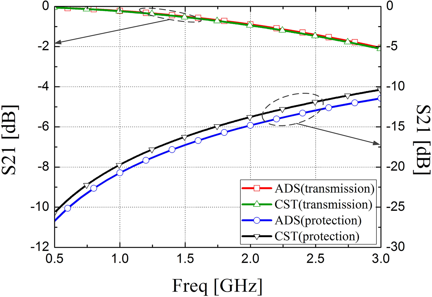
The results of equivalent circuit method carried out by ADS is shown in Fig. 5. The insertion loss is <1 dB below 2 GHz when all diodes are cut-off, and the transmission attenuation is more than 15 dB when all diodes are on. The transmission capability of SFSS presents switchable characteristic in frequency domain. Besides, the results of full-wave simulations conducted by the CST MWS (Frequency Domain Solvers, Boundary Conditions – Unit Cell) are also presented in Fig. 5. The Unit Cell boundary condition, which virtually repeats the modeled structure periodically in two directions up to infinity, is based on Floquet-mode method. To avoid placing the diodes at the boundary, we make a translation to the model. Due to the repetition and extension of Unit Cell boundary condition, the simulation results are reliable. The simulation results of equivalent circuit method are consistent with full-wave simulation results achieved by CST MWS.

Fig. 5. Simulated transmission coefficient of the SFSS radome.
The transmission characteristic of SFSS changes with the switch of diodes. Before the conduction of diodes, the insertion loss is <1 dB below 2 GHz so that the signal passes though the SFSS with little attenuation. Therefore, we call this state of SFSS as transmission. When all diodes are on, the transmission attenuation is more than 15 dB in L band. So most of the energy of the incident wave is reflected, thus protecting the electronic equipment behind the SFSS. Similarly, we call this state as protection.
Surface current distributions
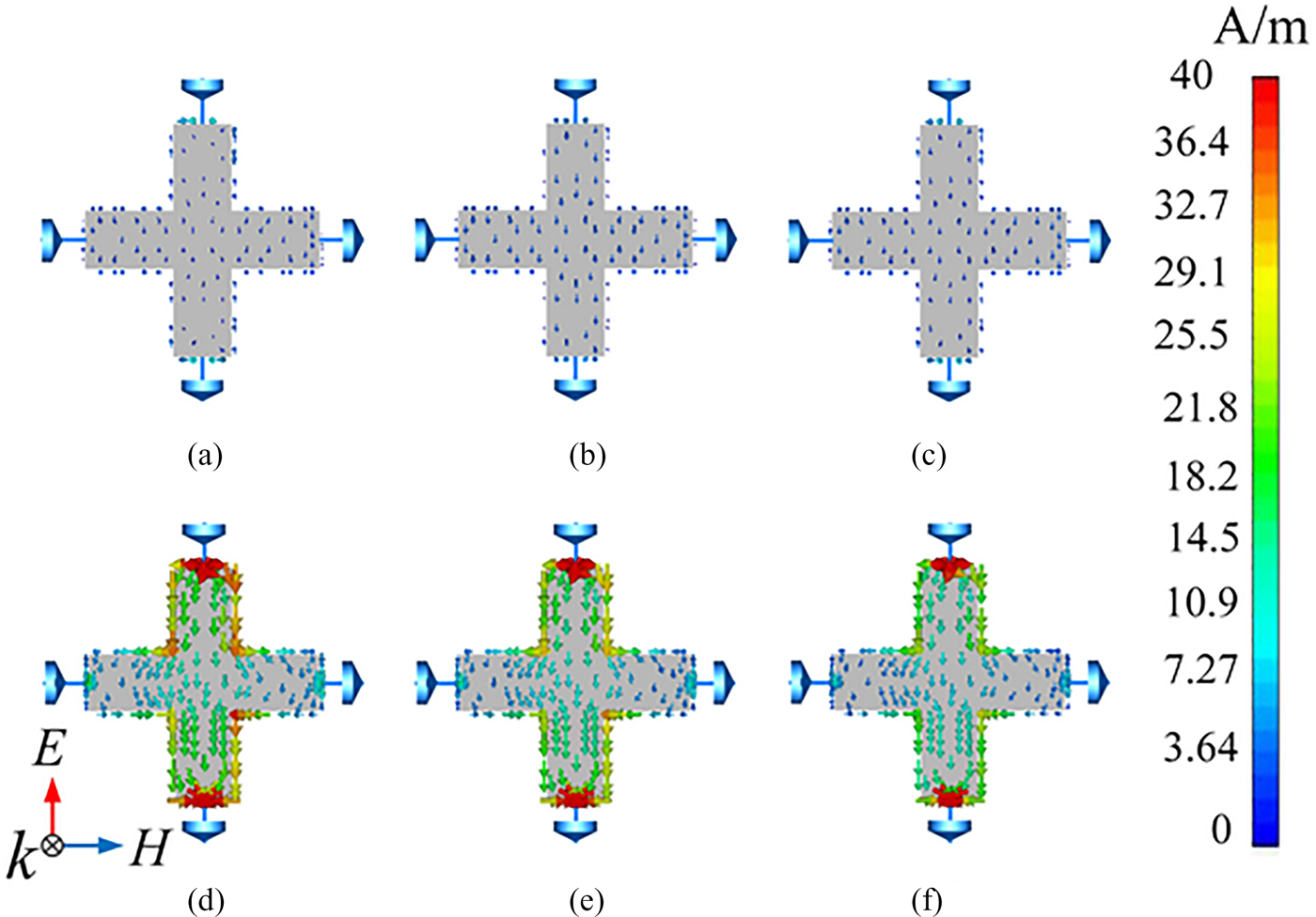
To give a further analysis to the physical mechanism, the surface current distributions at 1.25, 1.5, and 1.75 GHz are shown in Fig. 6. The direction of arrows represents the direction of the surface current density. Clearly, the surface current flows along the direction of the electronic field. In transmission mode, the surface current is so small that the electric field excited by metallic crosses is rather weak. As a result, the SFSS has almost no influence on incident wave. In contrast, the strong surface current is distributed along the edge of the patch, thus producing a strong scattering field. On the incoming side, the scattering field forms strong-amplitude reflection. On the other side, it is overlapped with the incident wave, making the total field approach zero.

Fig. 6. Distributions of surface current. (a) Transmission 1.25 GHz, (b) transmission 1.5 GHz, (c) transmission 1.75 GHz, (d) protection 1.25 GHz, (e) protection 1.5 GHz, (f) protection 1.75 GHz.
Prototype fabrication and measurement
S parameters
As the photograph shown in Fig. 7, a prototype of SFSS radome is fabricated. The overall size of the radome is 320 mm × 320 mm. The cross-patch array is printed on typical Teflon substrate. In the evaluation of shielding effects, it is difficult to measure the S 21 when the diodes are activated by high-energy incident wave. So we adopt the DC bias when measuring the shielding effect of protection mode. All the diodes at the same edge are connected with each other through a rectangular mental patch. DC voltage is loaded on a pair of parallel patches to switch the cascaded diodes, thus changing the working condition of SFSS. Four rectangular patches around the sample are isolated from each other to ensure the effectiveness of biasing. However, in the high-power microwave experiment, the PIN diodes realize ON state through the induced voltage caused by high-energy incident wave instead of DC bias, so the bias network is unnecessary.
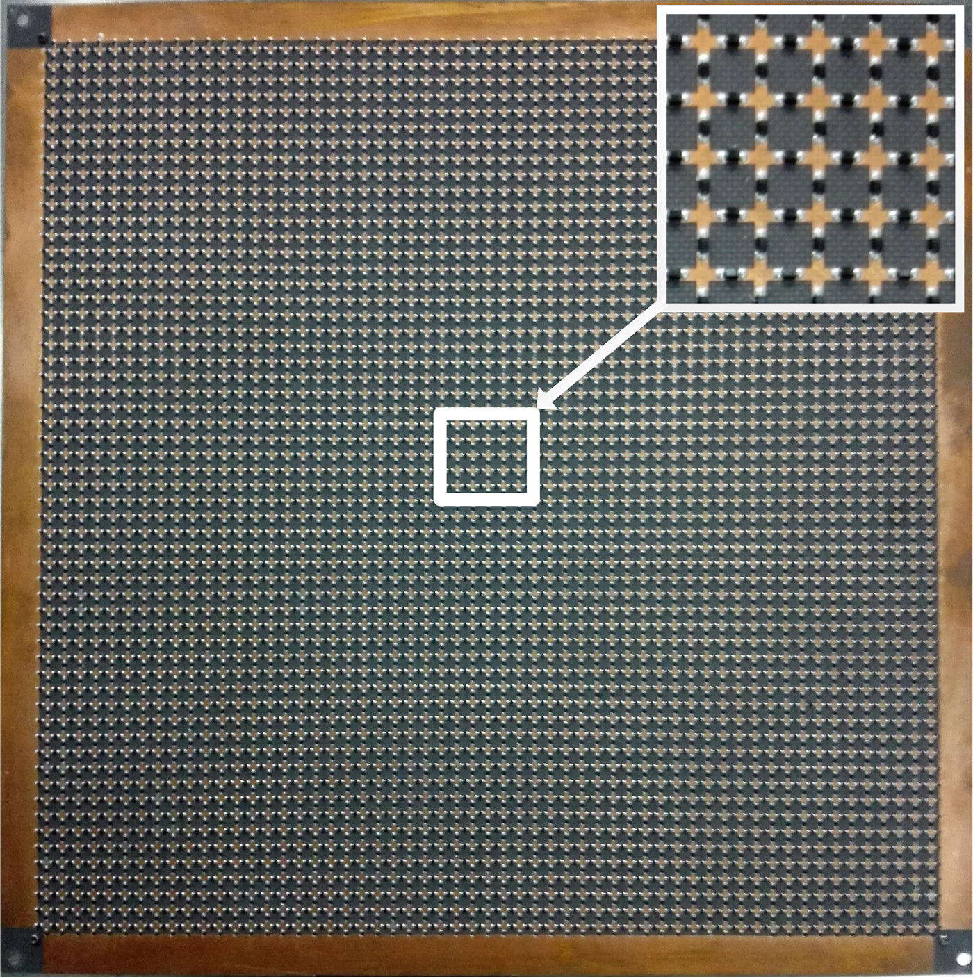
Fig. 7. Photograph of the SFSS prototype.
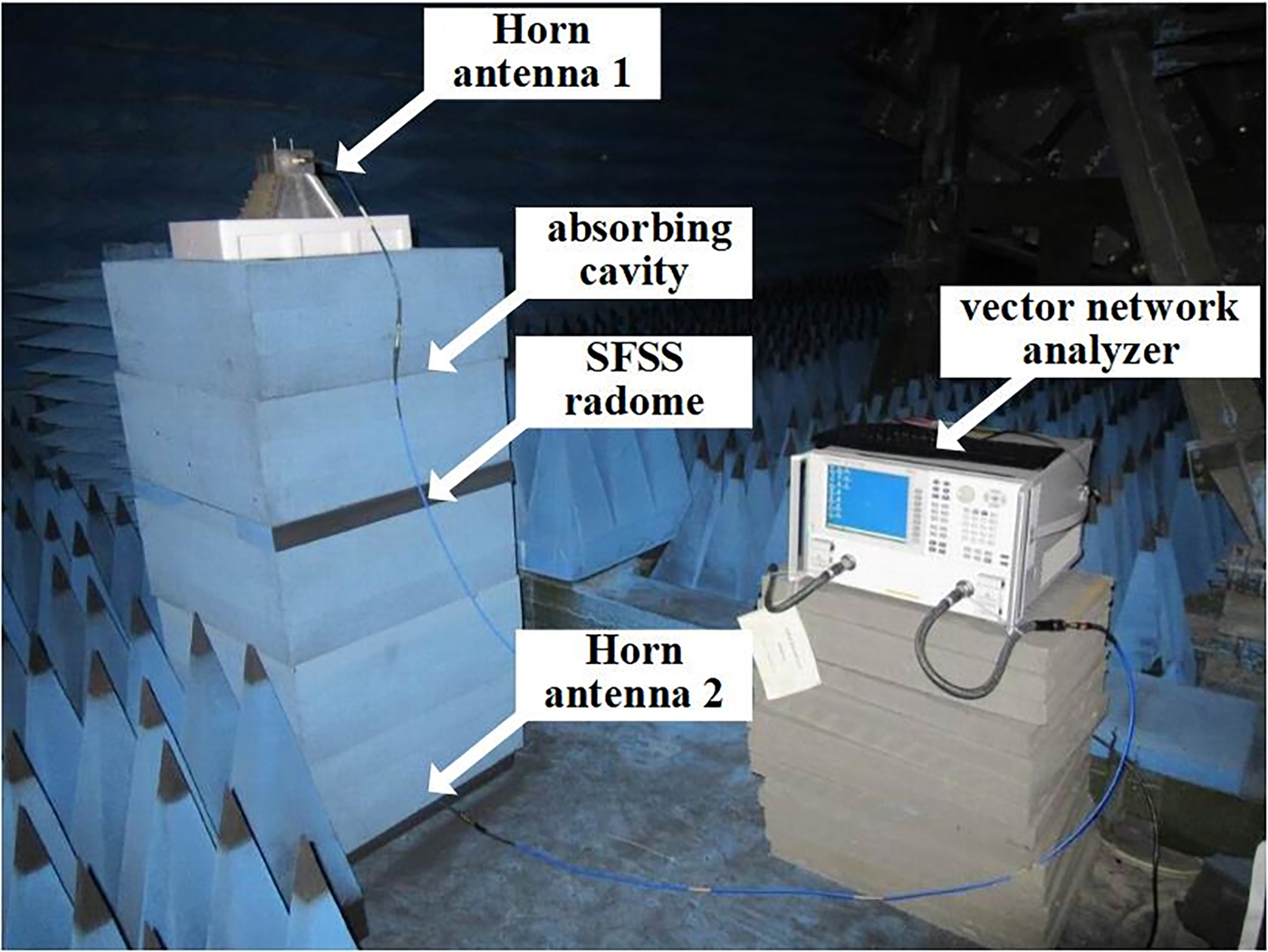
The representation of absorber measurement system model is shown in Fig. 8. This method can avoid the measurement error caused by edge diffraction and edge contact requirement in the nested reverberation chamber and the standard ASTM cell [Reference Marvin, Dawson, Flintoft and Dawson15]. The absorbing cavity is stacked by AEMI AEL-9.0 absorbing materials with thickness 229 mm. The outer and inner sides of the cavity are 609.6 and 300 mm, respectively. Two linearly polarized horn antennas operating from 0.5 to 18 GHz are aligned with identical polarization direction. The distance between transmitting antenna and the measured object is 0.458 m. The transmission coefficient is measured by Keysight vector network analyzer PNA-X.

Fig. 8. Photograph of the absorber measurement system.
Figure 9 gives the measured and simulated transmission coefficients of the SFSS in different modes. The insertion loss in measurement is below 2 dB in the transmission mode and the transmission attenuation reaches 18 dB in the protection mode from 0.5 to 2 GHz. The trends of measured results agree well with the curves obtained by full-wave simulation and the discrepancy of results is mainly caused by the deviation of fitted parameters of diodes and errors of measurement.
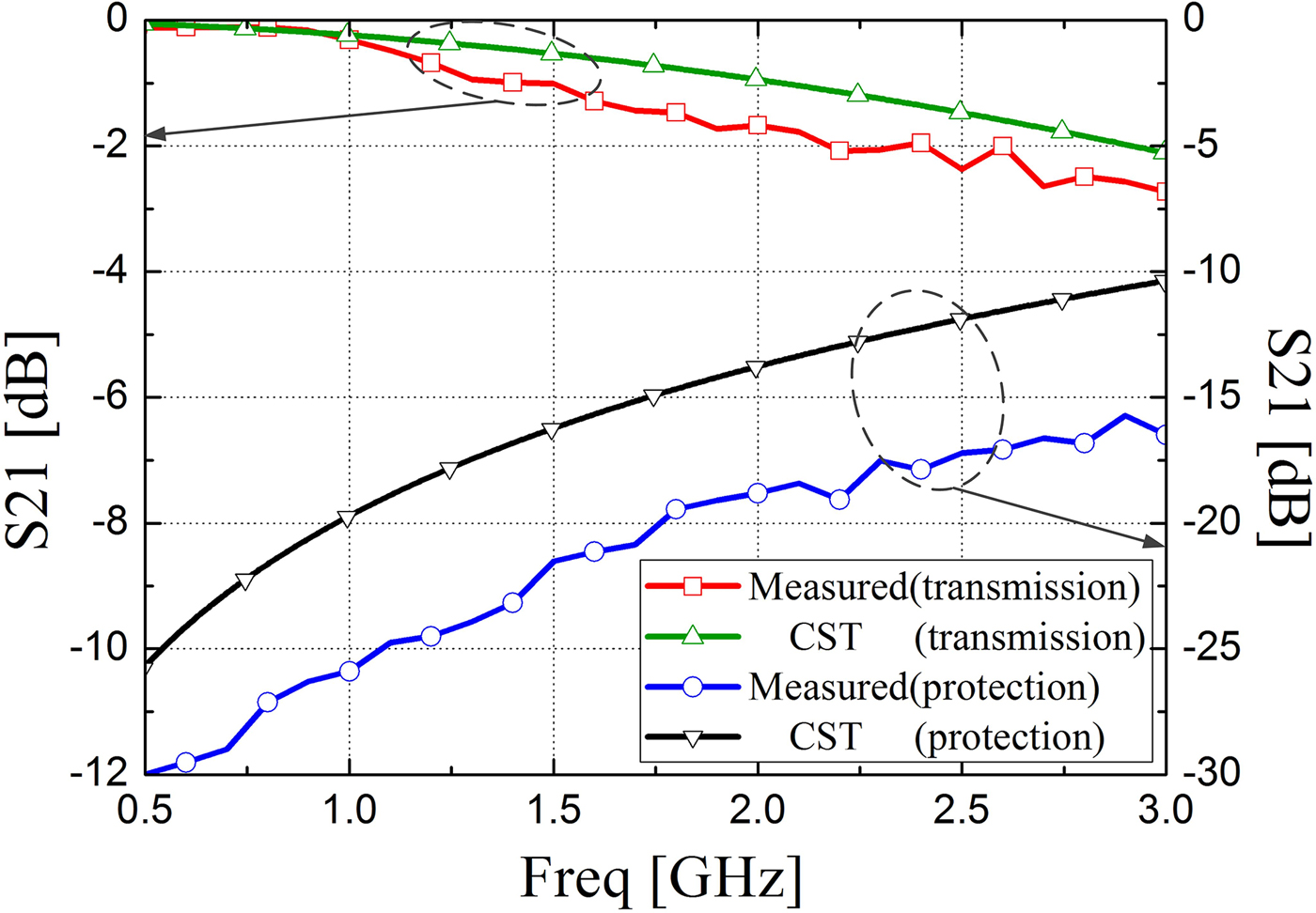
Fig. 9. Comparison of simulated and measured transmission coefficients of the SFSS radome.
High-power microwave experiment
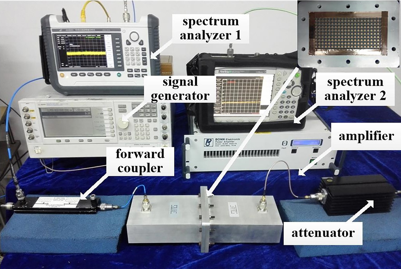
According to your comment, we carry out an experiment to explore the power for the activation of the diodes, instead. The system shown in Fig. 10 is used to observe the non-liner response and the breakover threshold of BAP 51-02. The signal engendered by signal generator Agilent 8267D is magnified by amplifier BONNBLMA 0502-70. Spectrum analyzer CETC 41st AV4023 monitors the signal entering the coupler RLC Electronics M-2594 and another spectrum analyzer Anritsu MS2038C works as a receiver. The device consisted of a pair of parallel diodes with opposite polarity is measured. The input and output power of the device can be obtained after calibration.
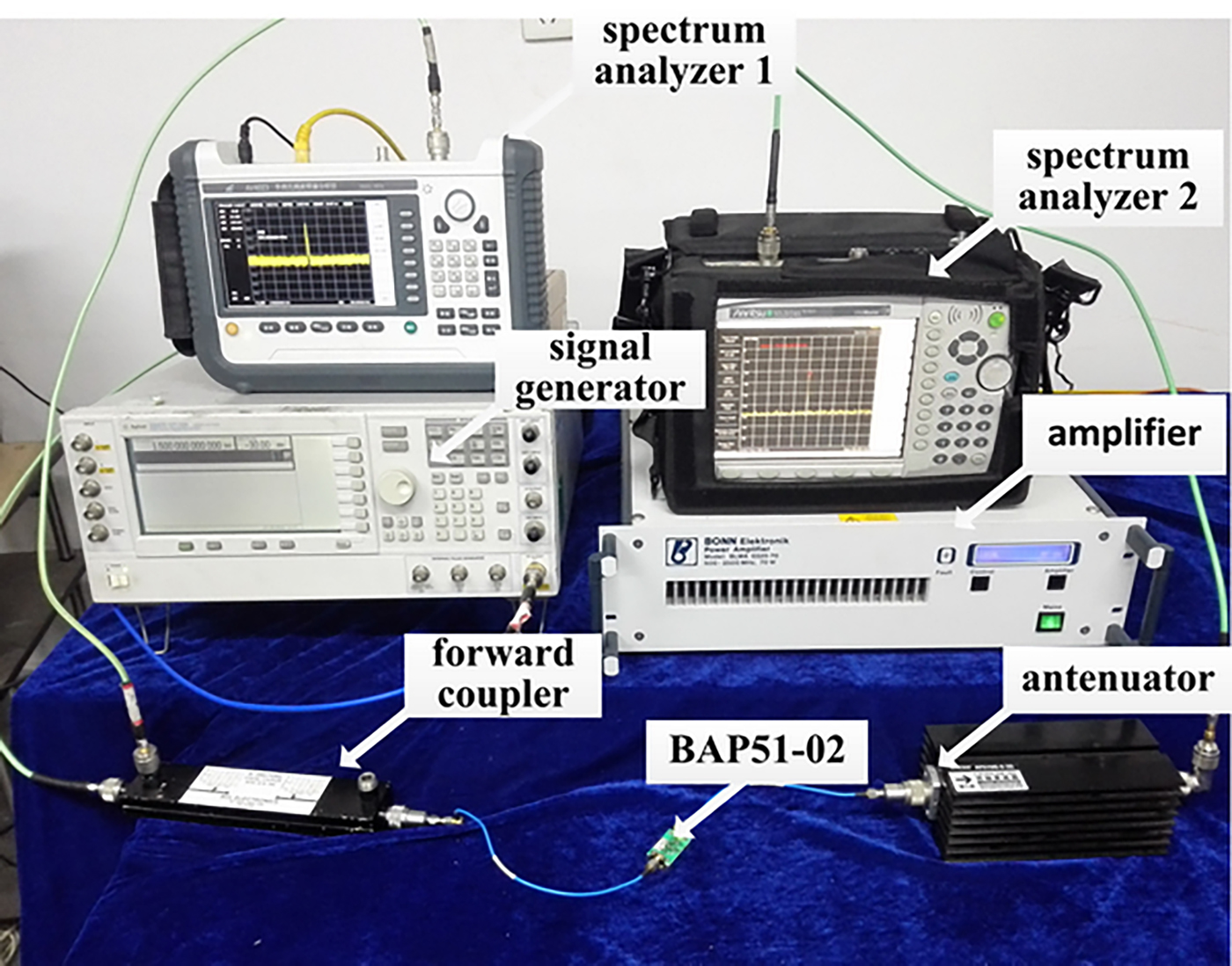
Fig. 10. Photograph of breakover threshold measurement of diode.
The power sweep for BAP 51-02 ranges from 0.5 to 2 GHz with step 0.5 GHz, and the response curves are shown in Fig. 11. The breakover thresholds of diodes at 0.5, 1, 1.5, and 2 GHz are 17.7, 24.1, 26.3, and 27.2 dBm, respectively. Besides, the turn-on insertion loss decreases with the rise of frequency, and the power drops steeply at the instant of conduction. When the period of input signal is much shorter than the carrier lifetime of I-layer, the I-layer appears in conductive modulation effects. Fewer charges are accumulated in I-layer with higher frequency, and it leads to the increase of carrier lifetime, resulting in a higher breakover threshold.
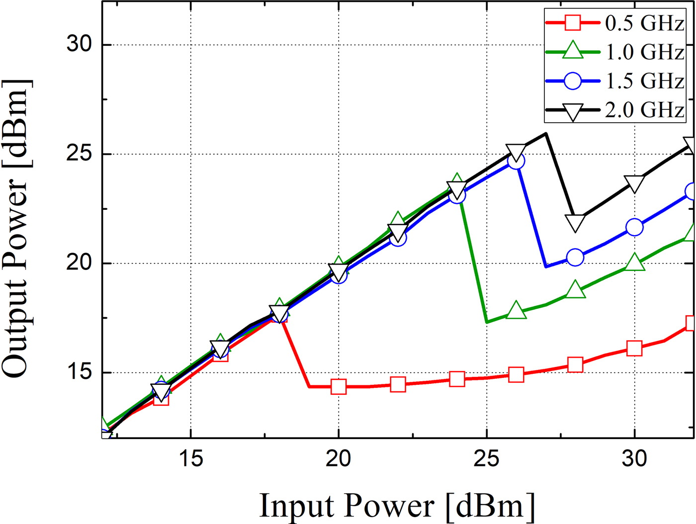
Fig. 11. Breakover threshold of BAP 51-02 at different frequencies.
The rectangular waveguide method shown in Fig. 12 is adopted to verify the self-actuated function and the shielding effectiveness of radome [Reference Liu and Behdad16]. The standard waveguide WR430 substitutes diodes of Fig. 10, and an SFSS sample (21 and 10 units, respectively) is placed in it with good electrical connection.

Fig. 12. Photograph of the waveguide measurement system.
The incident frequency is 1.75 GHz, which ensures single-mode propagation in the waveguide. The transmission properties with different input power are shown in Fig. 13. The attenuation imposed by waveguide reaches 1.7 dB and the insertion loss of the SFSS is about 2 dB before the breakover of diodes, so there is little attenuation for the transmission of incident wave. However, when the input power approaches 43 dBm, which means the intensity of electric field approaches 2853 V/m, the insertion loss increases sharply since the electromagnetic wave starts to trigger the diodes efficaciously. The shielding effect reaches 12 dB as the input power increases to 55 dBm. In other words, when the intensity of electric field in the cross-section of the waveguide approaches 11358 V/m, most of the energy is reflected by SFSS. The attenuation is lower than the result measured in the protection mode with DC bias. Exploring its causes, some diodes cannot be triggered due to the inhomogeneity of the transverse electromagnetic field in the waveguide.
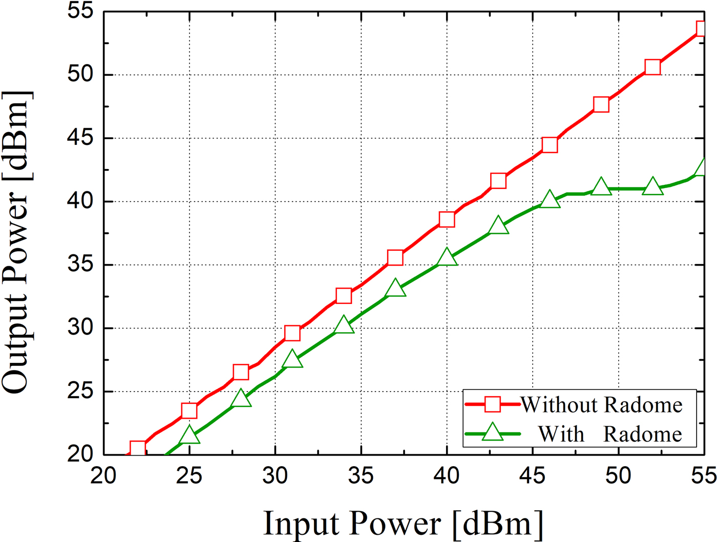
Fig. 13. Transmission properties of the SFSS radome with different input power.
Integration analysis
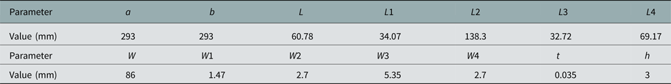
A quaternary microstrip antenna array is fabricated to study the effects of the radome on its performance. The structure of the antenna is shown in Fig. 14. It is printed on a standard Teflon substrate with a thickness 3 mm and works at 1.48 GHz, within the operating band of the radome. The antenna is placed in an aluminum shielding box covered by the SFSS radome. The radome and the antenna are separated by a foam layer with the thickness of 30 mm so as to reduce the influence of near-field coupling. The dimensions of antenna are showed in Table 5.
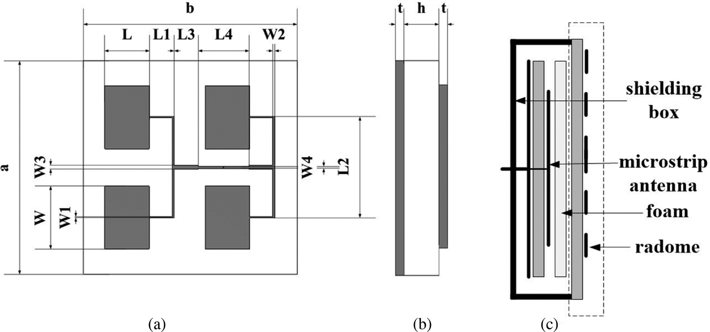
Fig. 14. Structure of the microstrip antenna. (a) Front view, (b) side view, (c) integration structure.
Table 5. Dimensions of the antenna
SFSS is used to protect the electronic devices from irreversible damage instead of ensuring the antenna work normally when the high-power electromagnetic wave irradiates. The S 21 of protection mode shown in Fig. 9 and experience in the waveguide shown in Fig. 13 have proved that SFSS can reflect most of the energy under that condition. Therefore, the integration analysis focuses on the effects of radome on antenna performance in small signal (Fig. 15).
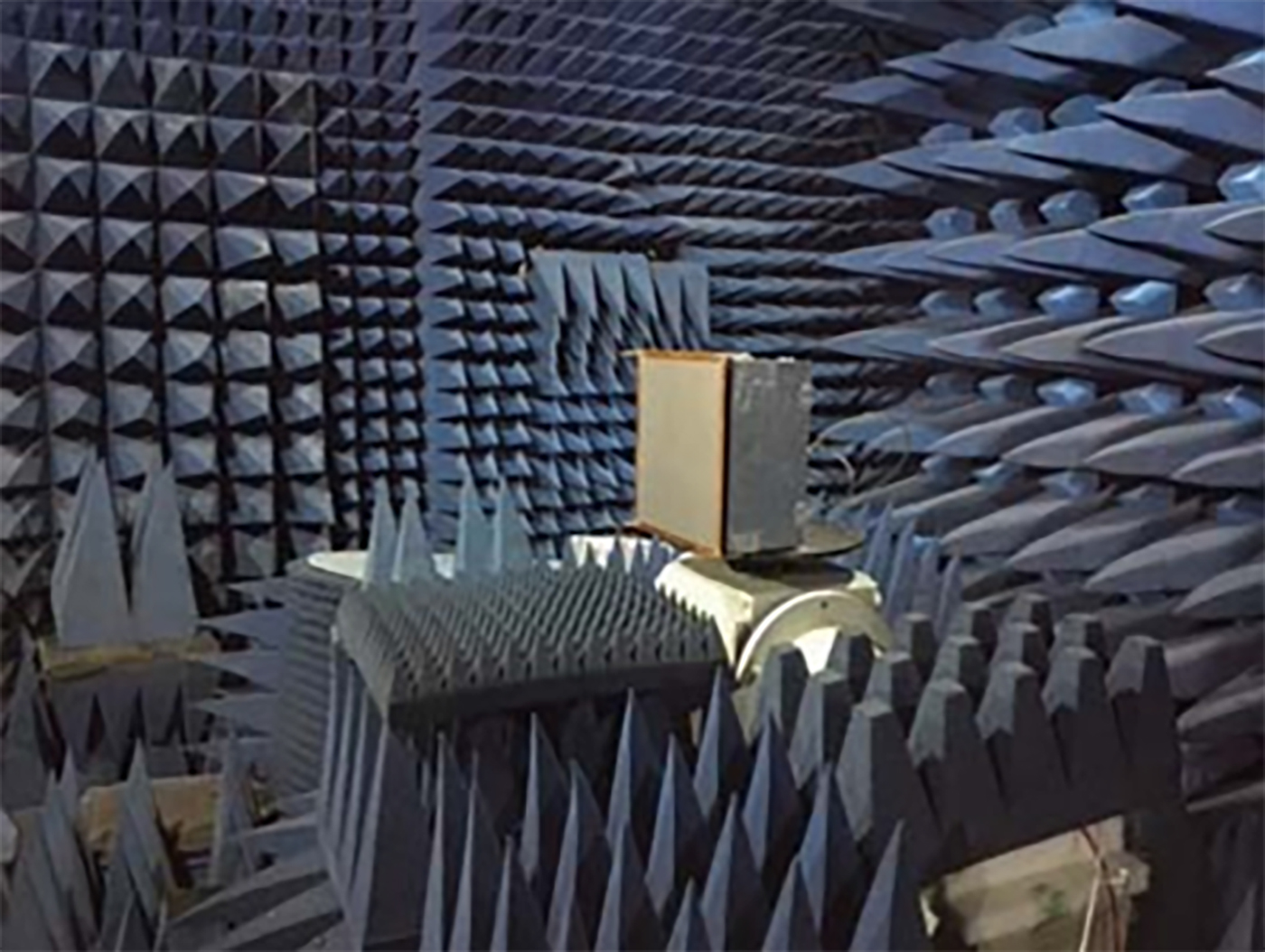
Fig. 15. Photograph of the antenna measurement.
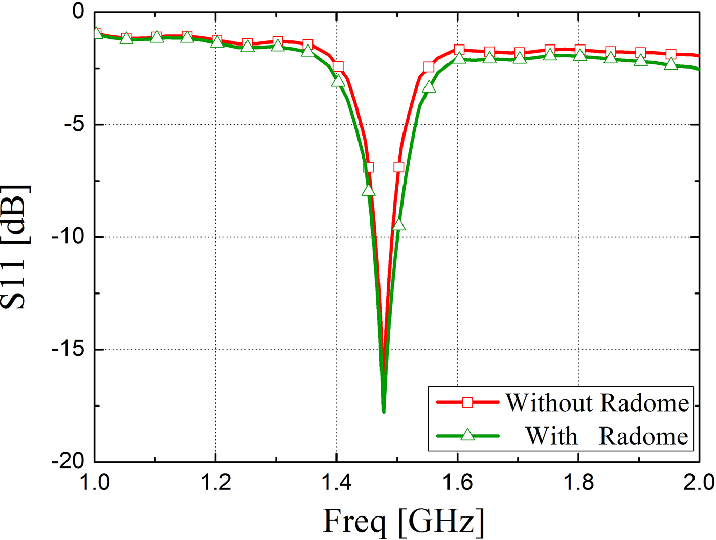
Energy of signals transmitted or received by electronic and electrical systems is rather low, so all of diodes are cut-off. The reflection coefficient and radiation pattern of the antenna with and without the SFSS radome are measured in the microwave anechoic chamber. From the measured S 11 shown in Fig. 16, the antenna with radome is resonant at the 1.48 GHz with better matching. The normalized H-plane antenna radiation pattern in the upper half space at 1.48 GHz is given in Fig. 17. Although there is a 0.69 dB insertion loss due to the attenuation of the radome, it can be seen that the SFSS radome has little effects on the antenna radiation pattern. When the antenna acts as a receiver, the SFSS can work normally. The microstrip antenna acts as a receiver in the experiment. According to reciprocity theorem, when transmitting small signals, the performance of antenna will not be affected by the radome as well.

Fig. 16. Reflection coefficient of the antenna without and with radome.
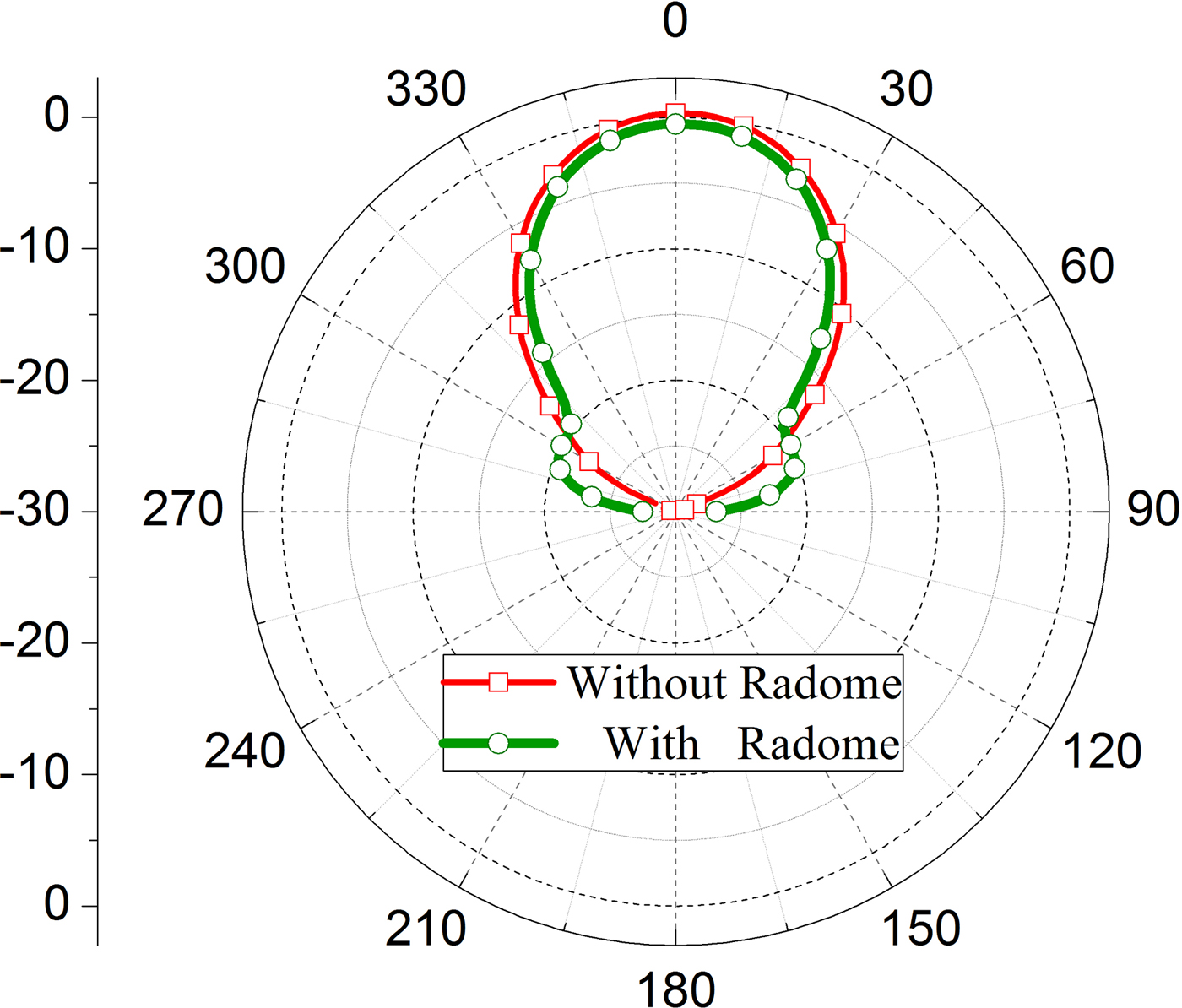
Fig. 17. Normalized radiation pattern of the antenna without and with radome (upper half space).
Conclusion
In this paper, a planar self-actuated frequency-selective radome with switchable property is designed and fabricated. It is integrated with a microstrip antenna to construct a system. Experiments show that the radome is transparent to low-power waves, while opaque to highly energetic wave from 0.5 to 2 GHz, which agrees well with the simulation results. The self-triggered switchable characteristic is verified in a waveguide testing system, and the attenuation of incident wave reaches 12 dB. Moreover, the radiation performance of the antenna operating at 1.48 GHz remains almost unchanged when the power of the incident wave is lower than the switching threshold.
 Qihui Zhou was born in Hunan, China in 1991. He received the B.S. and M.S. degrees in Electrical Engineering from the National University of Defense Technology (NUDT) in 2014 and 2016, respectively. He is currently working toward the Ph.D. degree at NUDT. His research is focused on FSS and metamaterial absorber.
 Peiguo Liu was born in Shanxi, China in 1969. He received the B.S. and M.S. degrees in Electromagnetic Field and Microwave Technologies and the Ph.D. degree in Communication and Information System from the National University of Defense Technology (NUDT), Changsha, China, in 1990, 1994, and 2000, respectively. From 2004 to 2005, he was a visiting scholar in the University of Calgary, Canada. He is currently an NUDT Professor, and his research is focused on electromagnetic radiation, scattering, and electromagnetic compatibility.
 Bo Yi was born in Chongqing, China in 1987. He received the B.S. and M.S. degrees in Electrical Engineering from the National University of Defense Technology (NUDT) in 2010 and 2013, respectively. He is currently working toward the Ph.D. degree at NUDT. His research is focused on EMC and antenna design.
 Dingwang Yu was born in Jiangxi, China in 1984. He received the B.S. and M.S. degrees in Radar Engineering from the Air Force Engineering University (AFEU) in 2008 and 2013, respectively. He is currently working toward the Ph.D. degree at NUDT. His research is focused on EMC and metamaterial design.