


I. INTRODUCTION
After that the U.S. Federal Communications (FCC) defined bandwidth of 3.1–10.6 GHz for commercial wireless communications [1], ultra-wideband (UWB) technology with high speed as wireless transmission developed. However, there are many challenges in the design of UWB than narrowband antennas. One of the most important challenges is the existing of frequency bands such as WLAN and WiMAX in this frequency range. That in this frequency range causes interference between UWB systems and other systems. For the same reason and in order to solve this problem, in recent years antennas with the ability of annoying frequency band rejection have attracted special attention. Some recent cases have been reported in [Reference Zhang, Zhong, Liang and Du2–Reference Rahanandeh, NoorAmin, Hosseinzadeh, Rezaei and Rostami15].
In [Reference Zhang, Zhong, Liang and Du2], the notched band is created using a beveled square monopole with a U-shaped slot in the microstrip feeder. In [Reference Valizade, Ghobadi, Nourinia and Ojaroudi3], a single band-notched function is provided by etching a П-shaped slot on the square radiating stub. A notched band function is created by attaching a pair of parasitic rectangular strips on one side of the slot antenna [Reference Zhang, Yin, Ma, Wang and Xiao4]. Using two types of simple slots cut on the radiating patch a notched band function is created [Reference Chen and Ku5]. In [Reference Nasrabadi, Rezaei and Saghayi6], a band rejected function has been proposed by defected ground structure for UWB applications. Most antennas designed with the capability of bands rejection are designed to remove a frequency band, for example WLAN (5.15–5.825 GHz), WiMAX (3.3–3.7 GHz), or both frequency bands. The advantage of the antenna designed in this paper, in addition to its small size, is the ability of three frequency bands WiMAX, WLAN, and ITU rejection. This is for the first time that an antenna with the ability of removing ITU-band in small dimensions is built. One of the other advantages of this antenna is the ability of working in five different modes. Changing the working modes is done by PIN diodes used in the antenna structure.
In this paper, we use a rectangular patch with an H-shaped slot on its surface and two C-shaped arms on its sides to remove the three frequency bands. The pin diode is used to control the performance of removing frequency bands because of their small size, suitable couplings, and the cheap price. For DC biasing pin diodes, we used the narrow lines approximately 200 µm.
II. ANTENNA DESIGN AND CONFIGURATION
The proposed antenna structure is shown in Fig. 1. The antenna is arranged on an FR4 substrate material with permeability 4.4 and loss tangent 0.24 and the dimensions 28 × 28 × 0.8 mm3. For transmitting signals, the antenna is connected to a 50 Ω – SMA connector. The process of designing of the proposed antenna consists of two stages that are simulated and discussed.

Fig. 1. Geometry of proposed antenna: (a) side view, (b) top view, and (c) bottom view.
A) Design of UWB antenna with WIMAX band rejection
The first stage is related to the design of UWB antenna with WiMAX band-rejection capability. As it can be seen in Fig. 2, this antenna consists of a rectangular patch on which H-shaped slot is created and a defected ground structure with two rectangular slots with dimensions L and W. By PIN diode located into the H-shaped slot the rejection WiMAX frequency band process can be controlled. PIN diodes have the task of reshaping the slot and also changing the electrical length of the radiation patch. This means that when the diode is forwarded in the bias, H-shaped slots on the radiation patch is converted in two rectangular slots. This deformation creates a larger surface radiation patch for current flow and thus creates more resonance.
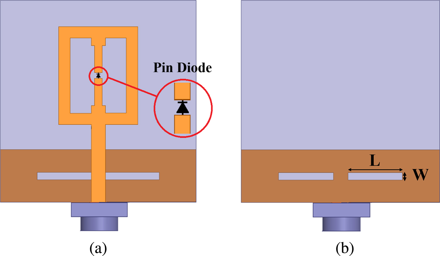
Fig. 2. Geometry of UWB antenna with WiMAX band rejection: (a) top view and (b) bottom view.
B) Design of UWB antenna with WiMAX, WLAN, and ITU bands rejection
In the second stage of designing, the capability of frequency band rejection of WLAN and ITU has also been added to the antenna. As seen in Fig. 3, by putting the two C-shaped arms around the patch and two slot L-shaped on the ground plane, two frequency bands WLAN and ITU can be rejected. L-shaped slots include one vertical arm with the length of L 13 and horizontal arm with the length of W 15. The width of these slots is uniform and equal to 0.8 mm. These two slots are located at the distance of 2.8 mm from the top of ground plane and are separated by the distance of 1.8 mm. The performance of rejecting these bands can be controlled by placing the two pin diode on the slot between C-shaped arms and the basic patch. To isolate the radio frequency (RF) signal from the DC-biasing voltage, three 100 pF DC blocking capacitors were utilized in the slots, as shown in Fig. 3(a).

Fig. 3. Geometry of UWB antenna with WiMAX, WLAN, and ITU bands rejections: (a) top view and (b) bottom view.
To optimize the antenna features, a parametric study is performed on the important parameters. The final dimensions of the antenna are shown in Table 1.
Table 1. Final dimensions of the proposed antenna.

C) Equivalent circuit
Figure 4 illustrates the equivalent circuit of the proposed antenna around the notch bands. To realize this circuit, let us start from the feed port of the proposed antenna. Since the branches are a quarter-wavelength long at their own resonant frequencies, three LC shorted ways, i.e. (L 1, C 1) with resonant frequency at 3.5 GHz, (L 2, C 2) with resonant frequency at 5.5 GHz, and (L 3, C 3) with resonant frequency at 8.25 GHz, emerge when one looks into the circuit from the feed port. According to the formulas
 $$Z = R + j\left( {\omega L - \displaystyle{1 \over {\omega C}}} \right),$$
 $${\omega _0} = 2\pi \, {f_0} = \displaystyle{1 \over {\sqrt {LC}}}.$$
When the circuit is operating at its resonant frequency, we have,
 $$Z = R + j\left( {{\omega _0}L - \displaystyle{1 \over {{\omega _0}C}}} \right) = R + j0, \quad {\rm as} \quad {\omega _0}L = \displaystyle{1 \over {{\omega _0}C}}\;.$$
The imaginary part of its impedance becomes zero, just like equation (3) shows. For a circuit that consists of ideal L and C, the circuit impedance will become zero, i.e. R = 0, when it works at its own resonant frequency. As Fig. 4 shows, the radiation resistance RA will be shorted at 3.5 or 5.5, or 8.25 GHz, when one looks into the equivalent circuit of the proposed antenna from the feed port. This means that the impedance of the proposed antenna is mismatched at the 3.5, 5.5, and 8.25 GHz, so the band-notched characteristics of the proposed antenna is achieved. The input impedance of a single C-shaped stub to the radiating edge can be given as
 $${Z_S} = {R_{slot}} + j{X_S}\;,$$
where R S is the real part of equation (4) and equivalent to radiation resistance of the slot, and imaginary part X S is the input reactance of the stub. In the present analysis, only the capacitive reactance X S is considered and the value of R S is very small and can be neglected. In this circuit, the C-shaped stub is taken as a capacitive reactance on antenna. In this study, the capacitive reactance is taken parallel to the reactance of the antenna for wideband characteristics.

Fig. 4. Equivalent circuit of the proposed antenna around the notch band.
III. USING RF PIN DIODES AS SWITCHES IN ANTENNA DESIGN
The PIN diodes switch can be used to design antennas with reconfigurable capabilities. PIN diodes in the RF frequency behave like a variable resistor. But they have a more complex circuit model for the state on and off. For both states ON and OFF PIN diodes have an L inductance. In the mode ON (forward biased) diode equivalent circuit is included a low resistance, R S . In the mode OFF (reverse biased) diode equivalent circuit is included of a parallel combination of R P , the reverse bias resistor and has C T the total capacitor. OFF-state resistance is calculated using the following equation.
 $${R_P} = \displaystyle{{{V_R}} \over {{I_R}}},$$
where I R is the reverse leakage current, when the test voltage V R is applied to the PIN diode. All amounts required to obtain a PIN diode equivalent circuit are shown in the data sheet. As seen in Fig. 5, the PIN diodes are modeled using two series lumped RLC boundary conditions in HFSS software.

Fig. 5. RF PIN diode: (a) equivalent circuit model and (b) HFSS model.
IV. RESULTS AND DISCUSSION
In this section, reconfigurable antenna with three band notch feature was built and numerical results, experimental input impedance, and radiation patterns are discussed. To simulate the antenna and get return losses Ansoft HFSS software is used [16]. In the first stage of designing to achieve a UWB antenna with band removal WiMAX capabilities, an H-shaped slot is used on a rectangular patch with two rectangular slots on the ground plane. The length of the rectangular slot has a large impact on antenna bandwidth. Figure 6 shows the return loss of the antenna for different values of the parameters.

Fig. 6. Simulated return loss of proposed antenna in Section IIA with different W 14.
As evident from the figure, by increasing W 14 parameter from 7.5 to 9 mm the antenna bandwidth increases but by increasing more than that, the antenna bandwidth will decrease again. The optimal value of this parameter as can be seen in the figure is 8.5 mm. In the second stage of designing, which the goal is to add the ability to remove ITU and WLAN frequency bands to the antenna in first stage, two arms around the original patch are used. Important parameters in this stage of designing are the size of C-shaped structure on each arm, and also the way two arms are connected to the main patch. Accurate determination of C-shaped structure on each arm has a direct impact on the rejected frequency band. Since each arm is to remove one of the frequency bands of WLAN and ITU, C-shaped structures also vary on each arm. A parametric study is done on the dimensions of C-shaped structures to achieve the above purpose. The results of this study are shown in Figs 7 and 8.

Fig. 7. Simulated return loss of proposed antenna for WLAN bands rejection with different L 3 and W 3.

Fig. 8. Simulated return loss of the proposed antenna for ITU bands rejection with different L 8 and W 11.
As show in Fig. 7, the effect of two parameters W 3 and L 3 from C-shape structure on removal of the WLAN frequency band is investigated. The optimal values of these parameters for the removal frequency range from 5.05 to 5.9 GHz, as can be seen in Fig. 6, are W 3 = 7 mm and L 3 = 5 mm.
In Fig. 8, the effect of two parameters W 11 and L 8 C-shape structure on removal frequency band ITU is reviewed. The optimal values of these two parameters for the rejection frequency range from 8 to 8.45 GHz are W 11 = 4.5 mm and L 8 = 3.5 mm. When trying to remove each frequency band WiMAX, WLAN, and ITU, the way of connecting two arms of the main patch is very important. The return loss of resulting measurement and simulated antenna presented in this paper is shown in Fig. 9.

Fig. 9. Measured and simulated return loss of the proposed antenna.
As the figure shows that there are similarities between the simulation results and measurement. However, some frequency shifts and wider range of the band notch are in the measured results which are due to difference between the actual PIN diode and capacitor with PIN diode and capacitor in the simulation model cause these differences. The antenna designed in this paper has the capability of working in five different modes. Figure 10 shows measured return loss of the antenna in five modes A, B, C, D, and E.

Fig. 10. Measured return loss of the proposed antenna in different modes.
As shown in Fig. 10, when all PIN diodes are turned off, the antennas in mode A, the antenna is able to cover the range of frequency 3–12 GHz. When only pin diode 1 turned ON, the antenna operates in mode B. In this mode, the antenna rejects frequency band 3.2–3.75 GHz. When only the diode 2 is turned on, the antenna works in mode C. In this mode, antenna will reject the 5.05–5.9 GHz frequency band. When only the diode 3 is turned on, the antenna will work in mode D. In this mode, the antenna is able to remove 8–8.45 GHz frequency band. In mode E, when all the diodes are turned on, the antenna covers the frequency band 3–12 GHz frequency band, while remove three frequency bands WiMAX, WLAN, and ITU. Figure 11 shows the measured radiation patterns including the co- and cross-polarization in the H- and E-planes. The radiation patterns in the H-plane are omnidirectional and uniform that this is a significant advantage for wireless systems.

Fig. 11. Simulated radiation patterns of the proposed antenna: (a) 4 GHz and (b) 6.5 GHz.
The measured gains of the antenna, from 3 to 11 GHz, are presented in Fig. 12. The figure indicates that the realized triple band-notched antenna has good gain flatness except in three notched bands. As desired, three sharp gains decrease in the vicinity of 3.5, 5.5, and 8.2 GHz.

Fig. 12. Measured gains of the proposed antenna.
The efficiency of the antenna is measured using the Wheeler cap method [Reference Tsai and York Robert17] and is also incorporated in Fig. 13. The antenna provides efficiency better than 75% in the UWB spectrum, while it drops to 25% in the notch band.

Fig. 13. Measured efficiency of the proposed antenna.
V. CONCLUSION
In this paper, a novel compact UWB microstrip antenna with switchable frequency bands for three band-notched has been introduced. In the proposed structure, a three band-notched function is provided by a rectangular patch with an H-shaped slot on its surface and two C-shaped arms on its sides. From the features of this antenna which can be noted are extended bandwidth, good radiation performance, and small dimensions. However, the main advantage of this antenna compared with the previous designed antenna is the ability to control intruder frequency bands rejection. This antenna can reduce the interference of other wireless communications with the UWB frequency band. All the mentioned advantages make this antenna a good choice of UWB systems.
ACKNOWLEDGEMENT
This work has been supported by the Semnan University. The authors would like to thank the Antenna Laboratory at Iran Telecommunication Research Center (ITRC).
 Esmail Nasrabadi was born in Esfarayen, Iran, in 1987. He received the B.S. degree in Electronic Engineering from Islamic Azad University, Bojnourd, Iran, in 2009. Currently, he is working toward the M.S. degree in Communication Engineering from Semnan University. His current research interests include antenna theory and design, reconfigurable microstrip antenna, and metamaterial microstrip antenna for wireless communication.
 Pejman Rezaei was born in Tehran, Iran, in 1977. He received the B.S. degree in Electrical Engineering from Communication Faculty, Tehran, Iran, in 2000, and the M.S. and Ph.D. degrees from Tarbiat Modarres University, Tehran, Iran, in 2002 and 2007, respectively. Currently, he is an Assistant Professor in Semnan University, Semnan, Iran. His current research interests include electromagnetics theory, antenna theory and design, and reconfigurable antenna.


