I. INTRODUCTION
Achieving simultaneously high-linearity and high-efficiency performances of radio frequency (RF) power amplifiers remains a very difficult challenge for the design of modern radio communication transmitters. Complex modulation schemes, required to increase spectrum efficiency, cause RF signals having large peak to average power ratios (PAPR). Consequently, power amplifiers have to operate at both high-power and large output power back-off with the best trade-off between linearity and efficiency.
Many research activities have been carried out during the past few years to investigate amplifier architectures providing an enhancement of linearity/efficiency trade-offs.
Doherty architecture remains one of the most popular solutions. One can note, for example, that dynamic bias control solutions of carrier and peaking cells of Doherty amplifiers have been studied in order to improve linearity performances [Reference Moon, Kim, Kim, Kim and Kim1].
Envelope tracking technique remains an important field of investigation to propose high-efficiency and linear amplification solutions with a major challenge to design high-current, high-efficiency and wideband drain bias modulators [Reference Kim, Kim, Cho, Kang, Park and Kim2–Reference Cidronali, Giovannelli, Vlasits, Hernaman and Manes6].
In this paper, we investigate a dynamic gate biasing technique applied to class-B GaN power amplifiers. Class-B operation of power amplifiers remains attractive because it offers the potential for high efficiency. Theoretically class-B operation could also achieve an excellent linearity if drain current IDS versus gate–source voltage V GS characteristic is linear above the pinch-off point [Reference Paidi, Xie, Coffie, Mishra, Long and Rodwell7]. Unfortunately, in a practical point of view, I DS/V GS characteristic is not piecewise linear around the pinch-off voltage. That results in poor linearity performances of class-B power amplifiers at large output power back-off. Nevertheless, one can observe that measured static I DS/V GS characteristics of GaN transistors tend to be almost piecewise linear around the pinch-off point. That presents an interest for high efficiency and linear class-B operation of GaN amplifiers.
The main idea presented in this paper is to apply a dynamic gate bias control to linearize the behavior of a class-B amplifier at low instantaneous envelope power. The gate bias voltage is pulled-up slightly above the pinch-off point to maintain a constant power gain. That principle has been already reported in [Reference Medrel, Ramadan, Nebus, Bouysse, Lapierre and Villemazet8]. A similar dynamic gate bias control proving linearity benefits in terms of two-tones and long term evolution (LTE) signal has been also reported in MOS technology [Reference Jin9].
The general principle of this work is quite similar to other works reported in [Reference Conway, Zhao, Asbeck, Micovic and Moon10, Reference Ye, Chiang, Chen and Sung11]. However, the strategy followed here is different because dynamic characteristics, instead of static AM–AM conversion, are measured for the extraction of the gate bias trajectory required to reach flat power gain conditions. This enables to take into account dispersive effects that are present in GaN-based devices such as thermal and trapping effects that may result in pinch-off voltage deviations [Reference Quere12]. To our knowledge it is the first implementation of a hybrid dynamic gate bias circuit applied to GaN-based class-B power amplifier.
Our work presented in [Reference Medrel, Ramadan, Nebus, Bouysse, Lapierre and Villemazet8] has been extended and is now presented in this paper. A gate bias circuit has been designed by using a wideband envelope detector along with ultra-fast operational amplifiers having clipping functionalities to process the envelope signal applied to the gate port of the RF power amplifier under test. Hybrid circuit implementation and performances are presented.
In Section II, the static characterization of the power amplifier under test is presented and the strategy of the proposed dynamic gate bias control is recalled. Section III is dedicated to the description of the dynamic gate biasing circuit implementation. In Section IV, measurement results of a 10 W – 2.5 GHz GaN power amplifier are given for two cases of signal excitation: a two-tone signal and a 16-QAM modulated carrier. Comparisons of power amplifier performances with a fixed gate bias voltage and a dynamic gate bias voltage are shown and commented. To conclude, future investigations are mentioned.
II. CHARACTERIZATION OF THE CLASS-B GaN POWER AMPLIFIER AND DYNAMIC GATE BIAS CONTROL STRATEGY
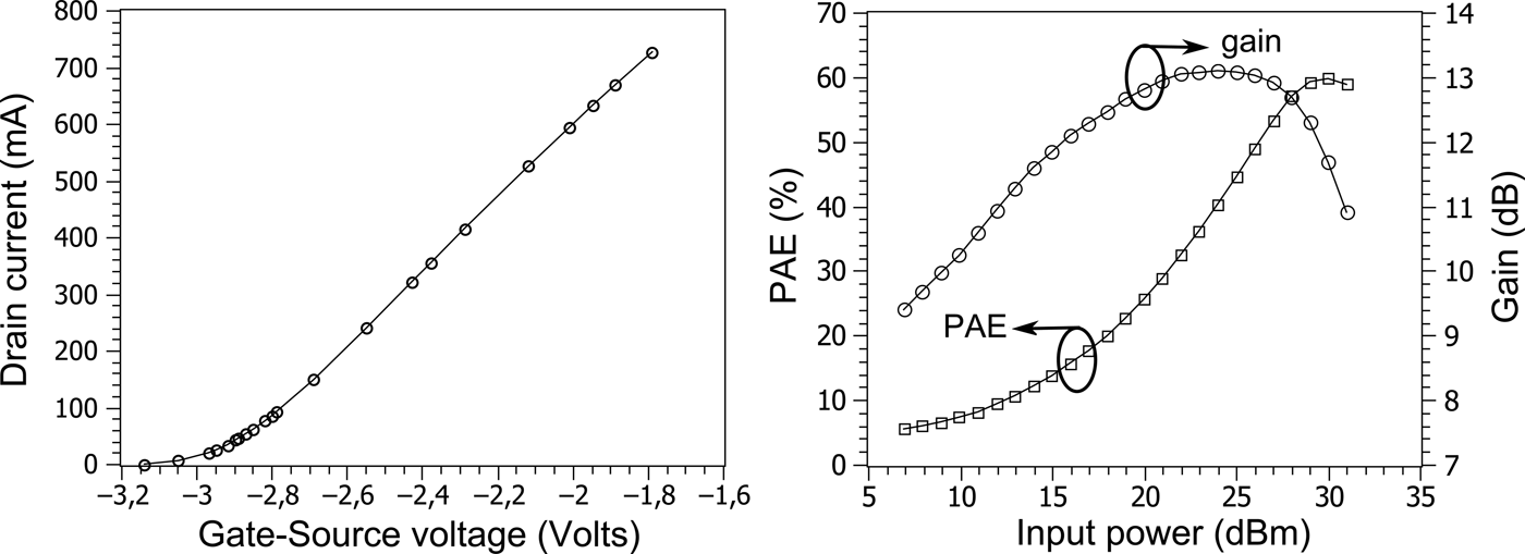
The GaN power amplifier used for this study is a test board CGH27015-TB from CREE [13]. The GaN HEMT used has a 3.6 mm gate periphery. The maximum drain current is about 1.8 A. Working frequency is 2.5 GHz. Large capacitances have been disconnected from the gate bias circuit to enable dynamic voltage variations. Static I DS/V GS characteristic at a drain voltage V DS = 28 V and power performances recorded for CW conditions and for the class-B gate bias point (V GSQ = −3.14 V, I DSQ = 0 mA) are given in Fig. 1.

Fig. 1. Static I DS/V GS characteristic at V DSQ = 28 V (left), gain and PAE versus output power for a CW tone at 2.5 GHz and a fixed gate bias at pinch-off V p (right).
When it is biased at the pinch-off voltage (V GSQ = −3.14 V) the power amplifier exhibits good power-added efficiency (PAE) performances but a poor and non-constant gain profile at low-power level that is prejudicial for linearity.
The simple idea to enhance linearity of the class-B amplifier at output power back-off is to implement a dynamic gate bias control as illustrated in Fig. 2.
Fig. 2. Principle of the proposed dynamic gate bias technique.
When the magnitude of the RF input signal is above a threshold voltage V TH the gate bias point is fixed to the pinch-off voltage V p = −3.14 V. When the magnitude of the RF input signal is below the threshold, the gate bias voltage is pulled-up slightly above the pinch-off voltage to get an increase of the small signal power gain. For that purpose, the magnitude of the envelope signal needs to be successively clipped at a value V TH, inverted and tuned at a minimum of −3.14 V by adding an offset. The resulting voltage signal is finally expanded by a linear coefficient α before being applied to the gate bias port of the amplifier under test.
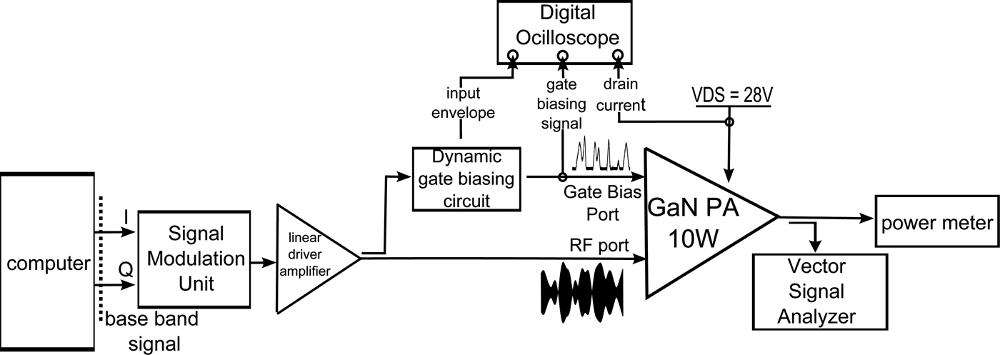
The experimental determination of an appropriate gate bias trajectory must be achieved when the amplifier is driven by non-constant envelope signals because measured power gain profiles are impacted by dispersive effects caused by self-heating and trapping. Therefore a time-domain envelope setup is used for the characterization of dynamic AM–AM profiles. The block diagram of the setup that we use is given in Fig. 3.
Fig. 3. Block diagram of the experimental setup used to demonstrate the proposed dynamic gate biasing technique.
The envelope gain versus instantaneous magnitude of the base band signal is measured when the power amplifier under test is driven by a 2-Msymb/s 16-QAM signal at 2.5 GHz. Measurement results are plotted in Fig. 4.
Fig. 4. Principle of the proposed dynamic gate biasing applied at low-level envelope magnitude under a 2 Msymb/s 16-QAM signal excitation.
In this figure, the horizontal dotted line indicates the flat gain profile that is targeted to enhance linearity performances. The appropriate value of the threshold voltage V TH is also identified along with the need for a dynamic gate bias control for instantaneous envelope levels smaller than V TH. For instantaneous envelope levels larger than V TH the gate bias voltage is kept constant at the pinch-off value V p.
III. GATE BIAS CIRCUIT DESCRIPTION AND IMPLEMENTATION
The architecture of the proposed dynamic gate biasing system consists in two different circuits. The first one is a commercially available envelope detector (Analog Device ADL5511). The main characteristics of this block are: DC – 6 GHz RF carrier operation, 130 MHz video envelope bandwidth, and a linear 1.46 V/V envelope conversion gain. The typical time propagation delay is 4 ns.
The aim of the second circuit is to process the detected envelope. For that purpose, wideband operational amplifiers (Texas Instruments OPA699ID) are used and realize clipping, inverting and offsetting operations, as shown in Fig. 5. The electrical characteristics of these operational amplifiers are 1 GHz gain-bandwidth product and 260 MHz video envelope bandwidth.
Fig. 5. Gate biasing circuit topology.
The DC-consumption of the whole implemented gate biasing circuit is about 300 mW.
A photograph of the built-in gate bias circuit connected to the 10 W GaN demoboard amplifier is presented in Fig. 6.
Fig. 6. Picture of the gate biasing circuit connected to the power amplifier.
IV. MEASUREMENT RESULTS
A) Time alignment
A main aspect and a starting point of the experiment is to evaluate as accurately as possible the time delay between the gate biasing path and the RF input path in order to compensate this time delay. For that purpose, a pulsed RF signal is used and a tunable delay line is inserted in the RF path as depicted in Fig. 7.
Fig. 7. Principle of the time alignment procedure.
A Lecroy digital sampling oscilloscope (DSO) [14] has been used for simultaneous measurements of signals at RF input port (plane 2) and gate bias port (plane 1). Figure 8 shows measurements recorded before and after the compensation of the delay between RF and gate bias paths. A 7.4 ns delay has to be compensated.
Fig. 8. Measured signals at planes 1 and 2: before delay compensation (top) and after delay compensation (down).
B) Two-tone measurements and intermodulation improvements
In a first step we used a two-tone test signal and performed third- and fifth-order intermodulation ratio measurements (C/I3, C/I5) to validate our proposed linearity enhancement technique. A two-tone signal with a center frequency of 2.5 GHz and a tone spacing of 2 MHz was used.
Figure 9 represents the time-domain waveforms of the input RF envelope and the appropriate dynamic gate-biasing signal. Time alignment was tuned to reach a minimum of third- and fifth-order intermodulation products.
Fig. 9. Measured time-domain waveforms: RF input signal envelope and gate biasing signal in the case of a two-tone signal excitation (center frequency = 2.5 GHz, tone spacing = 2 MHz, and output power = 32 dBm).
Figure 10 shows instantaneous AM–AM profiles and envelopes of the RF signal at the power amplifier output for different gate bias voltage waveform tunings. The first biasing condition corresponds to a fixed gate bias at the pinch-off value V p (class-B operation). The second one is obtained when gate bias voltage is voluntarily pulled-up too much above the pinch-off value toward a class-AB operation mode when the instantaneous envelope of the RF input signal is low. Finally, the last case corresponds to the optimal shape of the dynamic gate biasing.
Fig. 10. Instantaneous AM–AM characteristics versus instantaneous input envelope signal (left) and corresponding time-domain waveform of the output envelope signal (right). Ideal linearly amplified input envelope waveform is indicated by the dotted curve.
A time alignment between RF input signal and gate biasing signal was applied to obtain as much as possible closed curves with minimum hysteresis.
Figure 11 shows measurements of third- and fifth-order intermodulation ratios. PAE and DC consumption are plotted in Fig. 12. Improvement of intermodulation ratios of the order of 10 dB has been obtained for 8 dB output power back-off. Efficiency is slightly impacted, mainly due to the dynamic biasing that rises to class-AB at low envelope amplitudes. The overall PAE is slightly degraded due to a minor impact of DC-consumption of the dynamic gate biasing circuit, which is about 300 mW.
Fig. 11. C/I3 (left) and C/I5 (right) versus output power with and without dynamic gate bias.
Fig. 12. PAE of the PA with its gate bias circuit compared to fixed class-B condition (left) and DC consumption (right) versus output power.
C) Measurements with 16-QAM signals and EVM improvements
Measurements were also performed when the power amplifier was driven by a 2-Msymb/s 16-QAM modulated signal having a 8.5 dB PAPR.
Measured time-domain waveforms of the input envelope signal and the optimally tuned gate bias voltage are shown in Fig. 13. The dynamic gate bias voltage was tuned in order to get a maximally flat AM–AM instantaneous profile.
Fig. 13. RF input envelope and gate biasing signal in the case of a 16-QAM modulated signal (2 MSymb/s, 33 dBm output power).
Three cases of output signal envelopes measured for different gate bias trajectories are plotted in Fig. 14. Optimal gate bias profile condition can be seen in the zoomed region.
Fig. 14. Output signal envelopes for three different gate bias profiles: for a fixed gate bias at pinch-off V p (envelope distortion at low level can be observed). With a non-optimal dynamic gate bias trajectory (gate bias is deliberately pulled-up too much from class-B toward class-AB). Finally, the last one corresponds to an optimal gate bias tuning.
Figure 15 shows measured dynamic AM–AM profiles and output signal constellations along with measured EVM for the same three cases of gate bias trajectories. An optimal EVM value of 2% is obtained. We can clearly observe EVM degradation due to dispersions of inner symbols of the IQ constellation when the AM–AM profile is not flat at low level.
Fig. 15. Constellation diagrams and instantaneous envelope gain measurements. Fixed gate bias at pinch-off V p (left), non-optimal gate bias profile with too much gain at low level (middle) and optimal tuning of gate bias profile for a maximally flat gain (right).
Figure 16 shows PAE and EVM performances versus output power when the proposed dynamic gate bias technique is applied. Comparison is made with fixed gate bias voltage conditions from V GSQ = −3.2 V up to V GSQ = −2.6 V The PAE is slightly degraded at low level when a dynamic gate bias is applied but EVM performances are significantly improved.
Fig. 16. PAE (left) and EVM (right) versus output power when the optimal dynamic gate biasing signal is applied and when fixed gate bias conditions from class-B up to class-AB are applied.
Figure 17 shows the output spectrum measurement with a 2-MSymb/s 16-QAM modulated signal and with the proposed gate dynamic control applied. A 6-dB ACPR improvement is obtained at 34 dBm output power.
Fig. 17. Output spectrum measurement showing a 6-dB ACPR improvement. ACPR reduction can be clearly seen between fixed class-B operation and with dynamic gate biasing conditions.
V. CONCLUSION
A simple dynamic gate biasing technique that enables 10 dB IMD improvement, along with 6 dB ACPR and five points EVM enhancements with a 2-MSymb/s 16-QAM modulated signal has been demonstrated in this paper. The overall PAE is slightly degraded due to a minor impact of DC-consumption of the dynamic gate biasing circuit. This method is based on a quite simple processing of the instantaneous input envelope. The gate biasing circuit includes an envelope detector followed by operational amplifiers whose role is to perform clipping, offset, and gain adjustments to elaborate appropriate gate bias voltage profiles taking into account power amplifier dispersion effects.
Future works will consist to demonstrate the possibility of the proposed approach to improve the mitigation of low frequency memory effects such as trapping effects that are inherent to GaN-based devices. The design of the gate bias circuit will also be improved considering more accurately the non-linear transconductance profile of the PA under test. Then the application of the technique to multicarrier power amplifiers will be investigated.
ACKNOWLEDGEMENT
The authors would like to acknowledge French space agency (CNES) and Thales Alenia Space (Toulouse) for their financial support.
Pierre Medrel was born in Limoges, France in 1987. After obtaining his Master degree in electronic engineering he was working toward is Ph.D. at the XLIM laboratory. His main field of interest is high-efficiency microwave PA architectures and non-linear device characterization.
Audrey Martin received the Ph.D. degree from the Limoges University, France, in 2007. She is presently a teacher and researcher with XLIM Laboratory, University of Limoges. Her main research interests include active microwave and millimeter-wave circuit design, wideband power amplifiers and non-linear modeling techniques. She is also interested in the development of characterization and modeling of graphene devices.
 Tibault Reveyrand received the Ph.D. degree from the University of Limoges, France, in 2002. From 2002 to 2004, he was a Post-Doctoral Scientist with CNES (French Space Agency). From 2005 to 2013, he was a CNRS engineer at XLIM. In 2013, he joined University of Colorado at Boulder as a Research Associate. His research interests include the characterization and modeling of RF and microwave non-linear components and devices. Dr. Reveyrand was the recipient of the 2002 European GaAs Best Paper Award and is a member of the IEEE MTT-11 “Microwave Measurements” Technical Committee
 Guillaume Neveux was born in Civray, France, in 1976. He received the Diplome d'Etudes Approfondies (DEA) degree from the Universite Paris 11, Orsay, France, in 2000, and the Ph.D. degree in electronics and communications from the National Superior Institute of Telecommunications (ENST), Paris, France, in 2003. Since 2004, he has been with the Instrumentation Group, XLIM Laboratory, University of Limoges, France. His research interests include non-linear measurement with LSNA and the study of RF sampling systems.
Denis Barataud was born in Saint-Junien, France, in 1970. He graduated from the Ecole Nationale Superieure de Telecommunications de Bretagne, Bretagne, France, in 1994. He received the Ph.D. degree in electronics from the University of Limoges, France, in 1998. From 1998 to 1999, he was a Post-Doctoral Scientist with the Microwave Laboratory, Centre National dEtudes Spatiales (CNES), Toulouse, France. Since 2000, he has been with the XLIM laboratory, University of Limoges, Limoges, France, where he became an Assistant Professor in 2001. His research interests include the development of time-domain equipment and techniques for the characterization of non-linear devices.
 Philippe Bouysse was born in Aurillac, France, on September 18, 1965. He received the Ph.D. degree in communication engineering from the University of Limoges, Limoges, France, in 1992. Since 1992, he has been with the University of Limoges, Brive, France, as a Teacher and Researcher with the XLIM Laboratory. His main research interests are the modeling of microwave transistors and the design and optimization of microwave PAs.
 Jean-Michel Nebus received the Ph.D. degree in electronics from the University of Limoges France in 1988. Then he has worked for 2 years as a Project Engineer with Alcatel Space Industries, Toulouse, France. He is currently a Professor with the XLIM Laboratory, University of Limoges. His main research interests are power amplifier design and non-linear circuit characterization.
 Luc Lapierre was born in Clermont-Ferrand, France, in 1957. He received the Dipl-Ing degree from the Ecole Superieure d'Electricite (ESE), Paris, Gif sur Yvette, France, in 1980. In December 1981, he joined the French National Space Centre (CNES), Toulouse, France, where he was involved in microwave research activities mainly oriented on solid-state components. He also provides technical support in the development of microwave equipments for satellite payloads. He has been the Head of the Microwave Department, CNES, and is currently a Microwave Expert with the Microwave and Time Frequency Department, CNES.
 Jean-François Villemazet received the Engineer degree in electronics and Ph.D. degree in electronics from the University of Limoges, France, in 1989 and 1994, respectively. In 1989, he joined the Thomson Company, where he studied mixer optimization. In 1994, he joined Alcatel Space Industries, where he designed numerous monolithic microwave integrated circuits (MMICs) and was involved with transistor non-linear modeling.
Since 1998, he has been studying the design of linearizers and PAs for satellite payloads. In 2003, he was responsible for the MMIC design team of Thales Alenia Space, Toulouse, France. Since 2007, he has been responsible for a team dedicated to the advanced study of microwave equipments for satellite payloads. His research interests are non-linear microwave circuit design and computer-aided design (CAD) methodologies.