I. INTRODUCTION
Microstrip patch antennas are a good selection for standard mobile and satellite communication systems due to their interesting characteristics of low cost, small size and weight, conformability, and ease of manufacturing. The main barrier for utilizing these microstrip antennas in many purposes is their limitation of bandwidth. In recent years, much effort have devoted to the bandwidth improvement of microstrip antennas. The many techniques have been used to increase the bandwidth [Reference Bose and Gupta1–Reference Nasimuddin; Chen11]. Among them, multi-layer microstrip antennas have attractive characteristics in addition to broad bandwidth. The multi-layer configurations provide benefit of isolating spurious feed radiation due to using of a ground plane between feed line and patch [Reference Kidder, Ming-Yi and Chang10–Reference Meiguni, Kamyab and Hosseinbeig13]. At microwave frequencies, wideband operation of these antennas has been demonstrated using either single or stacked patch configurations.
In this paper, a multi-layer microstrip antenna is designed in order to have perfect impedance matching. The proposed antenna consists of three main parts: a transmission line, a ring slot, and a modified ring patch. The transmission line and the ring patch make two resonances close to each other and the patch dimensions change to achieve the perfect impedance matching in a broadband bandwidth. A sample of the antenna has been fabricated and tested. The results of simulations and measurements are in a good agreement. The proposed multi-layer antenna in addition to having a perfect impedance matching throughout broadband bandwidth has adequate gain, stable radiation pattern, good radiation pattern, and low cross-polarization.
II. ANTENNA CONFIGURATION
A new linear-polarized multi-layer microstrip antenna is shown in Fig. 1. This antenna utilizes a single ring patch, which is simpler when compared to coplanar or stacked parasitic patches. The feed substrate is Rogers 5880 with relative permittivity of 2.2 and thickness of 1.57 mm. It is common for broadband antenna to use a thick substrate with low permittivity, so an 8-mm air-filled substrate is applied between the ring slot and the modified ring patch. Finally, an FR4 upper substrate with thickness of 1.57 mm and relative permittivity of 4.4 was applied as the supporting substrate.

Fig. 1. Proposed multi-layer antenna (all units are in mm).
The antenna is designed using coupled resonances. In fact, the shape of transmission line along with the slot and the patch designs in a transmission line is a good choice to resonate along with the ring slot; the choice of cross-shaped transmission line also provides us with more variables to design with. Another resonance is produced by modified ring patch. This kind of patch which helps us to obtain the desired gain can easily provide a good resonance.
The dimensions of transmission line, ring slot, and modified ring patch are optimized to make these two resonances close together. The ring patch is designed in a way it can resonate in its second harmonic. This provides us with an opportunity to have higher gain. Moreover, it produces more variables in order to design better. For having two resonances close together, the internal and external radiuses of ring slot are 8 and 13 mm, respectively, and the dimensions of transmission line also have been given in Fig. 1. Now, shape and dimensions of the patch have to be designed in order to make perfect impedance matching. In fact, the patch is designed in the way it can improve the perfect impedance bandwidth.
In our proposed multi-layer antenna structure, design of patch is crucial. Among several tests, the ring patch is selected because it can make suitable impedance and gain bandwidths. An extra impedance bandwidth enhancement is obtained by deleting two 90° ring segments on the patch, as shown in Fig. 1. The radiuses of segments of shaped ring patch are very significant in the bandwidth. Figures 2 and 3 show the effect of two parameters of the modified patch. As shown in Figs 2 and 3, the parameters R and y can improve the impedance matching. In fact, they develop the value of two resonances of the transmission line and ring slot. The optimum values of R and y are 14 and 5.7 mm, respectively. We also optimized the open circuit length of the transmission line (s) to improve bandwidth. The optimum value for the parameter s is 1.6 mm. The proposed antenna was designed for broadband operations at the applications of perfect impedance matching.
Fig. 2. The effect of the deleted segment of the patch (R) on the impedance bandwidth.
Fig. 3. The effect of the parameter y on the impedance bandwidth.
III. SIMULATION RESULTS AND DISCUSSION
The antenna simulation is performed by high frequency structural simulator (HFSS) and computer simulation technology (CST) simulators. Figure 4 displays the simulated reflection coefficient of the proposed multi-layer antenna. It shows that good agreement was achieved between HFSS and CST simulations. It is seen that a bandwidth of 70% is obtained nearly from 3.35 to 6.95 GHz for |S 11| < −10 dB. It is evident that the impedance matching is excellent in intermediate frequencies in which the impedance bandwidth for |S 11| < −20 dB is almost 31% within frequency range of 4.7–6.42 GHz. It can be used in some applications that need perfect impedance matching. Here, our used application is active integrated antenna (AIA) which the antenna applies as load. In this application, the output load of the power amplifier (PA) that antenna is a part of has to be organized for optimum load of PA analyzed by pull–push analysis. As reflection coefficient (|S 11|) is less, the input impedance of antenna is closer to 50 Ω. For |S 11| < −20 dB, the input impedance is almost 50 Ω. Therefore, the reflection radiation wave is nearly zero. This has lots of advantages. First of all, the reflection radiation wave can cause serious problems. If the load of PA changes, the PA may has been shifted in an unstable position in smart chart, especially when the stability circles are close to the optimum load of PA in smith chart. When the input impedance of antenna is constant (|S 11| is very negligible), there is no worry about the stability. Furthermore, you can design your PA for its optimum load for all frequencies in the desired bandwidth. If |S 11| < −10 dB, in some frequencies, the load will run away from the optimum value and the efficiency and output power will decrease, but, if |S 11| < −20, you are sure that you have fixed the load for its optimum value because the value of load is almost constant over bandwidth frequencies. Additionally, in this situation the design of PA is very easy because you will not be worried about the output load. It was discussed in the previous section that in order to increase the bandwidth, it was applied the thick air-filled substrate, the resonant aperture and transmission line, and the modified patch. Figure 5 shows the impedance loci of proposed antenna for the variation of R and y.
Fig. 4. Simulated reflection coefficient of the multi-layer microstrip antenna by HFSS and CST simulators.
Fig. 5. Impedance loci of the broadband multi-layer microstrip antenna.
The two coupled resonances of transmission line, slot, and patch result in an impedance locus, which presents a dense loop around the center of the smith chart, illustrated in Fig. 5 for R = 14 mm in Fig. 5(a) and y = 5.7 mm in Fig. 5(b). As shown in Fig. 5, when R and y increase, the perfect impedance matching improves. This in turn means that the resistance of the antenna becomes close to 50 Ω and reactance decreases toward zero. Thus, with the increase of R and y and in turn approaching 50 Ω (the center of smith chart in Fig. 5), the loops of impedance loci become smaller and contract. In other words, when R and y increase, the reactance becomes smaller approaching zero and the resistance becomes close to 50 Ω. An antenna gain >6 dB has been obtained across the bandwidth and is depicted in Fig. 6. The maximum gain of the proposed antenna is 8.8 dB at the frequency of 5.25 GHz by HFSS simulator. It is seen that there is an adequate gain over the frequency range. In [Reference Harrington14], it is proved that the gain of an antenna depends upon its physical size compared to wavelength; so we selected the size of the ring patch so great that it operates at the second resonant and then we optimized dimensions. This explains the relatively high amount of the gain over the bandwidth. Figures 7–10 show the simulated results for E- and H-plane radiation patterns at 4.4 and 5.8 GHz by HFSS and CST simulator. They show that almost symmetric radiation patterns are achieved in both the E- and H-planes. The cross-polarization levels are adequate. At 4.4 GHz, the cross-polarization level in the 3-dB beamwidth is 18 dB under the co-polarization in the E-plane and 46 dB under the co-polarization in the H-plane, illustrated in Figs 7 and 8. But at 5.8 GHz, the cross-polarization level in the 3-dB beamwidth is 20 and 49 dB under the co-polarization in the E- and H-planes, respectively. The minimum difference between co- and cross-polarizations in the 3-dB beamwidth is about 18 dB, which is acceptable. The antenna can support many existing wireless services, broadband applications over frequency range of 4, 5, and 6 GHz, and multi-standard mobile communication systems.
Fig. 6. Simulated gain of multi-layer antenna by HFSS and CST simulators.
Fig. 7. Simulated E-plane pattern at 4.4 GHz.
Fig. 8. Simulated H-plane pattern at 4.4 GHz.
Fig. 9. Simulated E-plane pattern at 5.8 GHz.
Fig. 10. Simulated H-plane pattern at 5.8 GHz.
IV. EXPERIMENTAL RESULTS
A prototype antenna was fabricated and measured using an Agilent-8722ES Vector Network Analyzer. Figure 11 shows the top and bottom views of the fabricated prototype. Figure 12 depicts the measured reflection coefficient and gain of the fabricated antenna. The perfect impedance bandwidth for |S 11| < −20 dB is almost 34.7% throughout the frequency range of 4.4–6.25 GHz. For the pattern test of the antenna, we have used a standard antenna test set with a horn antenna as a source and 6 m away from the test antenna in an anechoic chamber. Over this frequency range, the gain is nearly stable and its value is above 7.5 dBi. As shown in Figs 13 and 14, the measured radiation patterns of E- and H-planes indicate that the minimum difference between co- and cross-polarization is about 13 dB in 3-dB beamwidth at 5.8 GHz, also, it is seen that the cross-polarization of the H-plane is negligible. Thus, it must be noted that these values may differ in other measurement runs. However, they prove that the cross-polarization is very low. These results show extreme linearity of the polarization of the H-plane.
Fig. 11. A fabricated prototype of the proposed antenna.
Fig. 12. Measured gain and reflection coefficient of the proposed antenna.
Fig. 13. Measured co- and cross-polarization of E- and H-plane patterns at 4.4 GHz.
Fig. 14. Measured co- and cross-polarization of E- and H-plane patterns at 5.8 GHz.
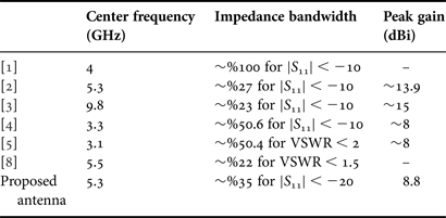
Table 1 has been depicted in order to compare the proposed antenna to the other multi-layer antenna. It is seen that our proposed antenna has broadband perfect impedance bandwidth and gain compared with that of the other aperture-coupled single-patch antennas. This broad bandwidth is achieved because of optimum design of the transmission line, ring slot, and shaped patch. The simulated results show that the radiation efficiency is greater than 93% over the bandwidth.
Table 1. Comparing the proposed design to the other linear-polarized multi-layer antennas.
IV. CONCLUSION
In this work, a broadband multi-layer microstrip antenna was presented. The broadband operation is a result of suitable design of the transmission line, slot, and patch. We applied a cross-shaped transmission line with a ring slot and a modified patch. The radiuses of segments and separated rectangular sections of the modified patch were critical in the design. The simulation and measurement results show that a broad impedance bandwidth of 70% for |S 11| < −10 dB has been obtained. There is also a perfect impedance matching bandwidth of 35% for |S 11| < −20 dB. Impedance loci diagram of the antenna illustrates a dense loop around the center of the smith chart. Maximum gain is 8.8 dB at the frequency of 5.25 GHz. The radiation pattern, radiation efficiency, and cross-polarization are also almost good on the impedance bandwidth. A measured minimum difference between co- and cross-polarization in the 3-dB beamwidth is 13 dB, which is acceptable.
 Mahmoud Abdipour received his B.S. degree in Electrical Engineering from the Islamic Azad University, Broujerd branch, in 2008, and the M.S. degree in Electrical Engineering from Islamic Azad University, Arak branch, in 2012. He has authored and co-authored several books, including Signals and Systems, Electrical Engineeing Dictionary, and Microstrip Antennas. He has translated two books, including Phased Array Antennas and Digital Signal Processing. He is the Editor of Communications Circuits (Nass Press, 2013 by Professor Abolali Abdipour). His interests are in microwave and millimeter-wave devices and circuits, microwave-integrated circuits, integrated antennas, wide-band and active antennas, phased arrays, and numerical methods in electromagnetics.
 Saba kazemi alishahi received her B.S. degree in Electronic Engineering from Razi University, Kermanshah, Iran, in 2006, and the M.S. degree in Electronic Engineering from Islamic Azad University, Arak branch, in 2012. She has worked as an instructor of various electronic courses in different branches of Azad University for 3 years. Her interests are in microwave and millimeter-wave devices and circuits, wide-band and active antennas, and phased arrays antennas.
 Kambiz Noormohamadi received his B.Sc. and M.S. degrees from Kerman University, both in Electrical Engineering in 1995 and 2012, respectively. His research interests are microwave and optoelectronic circuits. He has authored and co-authored two books, including Signals and Systems, and Signals and Systems Using Matlab. He has worked as an instructor of various electronic courses in different branches of Azad University for 7 years.