I. INTRODUCTION
Conventional reflective bandstop filters [Reference Wu, Amari and Resenberg1–Reference Qian and Tang8] have been used for suppressing unwanted signal in the frequency domain. One of the important design parameter in designing the bandstop filters is attenuation level at the center frequency. However, it is mainly limited by the Q-factors of the resonators employed in the reflective bandstop filters. Since a larger resonator has a larger Q-factor, a reflective filter must employ large resonators to achieve large attenuation at the center frequency. Hence, absorptive bandstop filter designs have been proposed to overcome the Q-limited attenuation performance at the center frequency [Reference Jachowski9–Reference Lee, Lee and Chappell14]. The absorptive bandstop filter design approach allows us to use low-Q resonators in achieving large attenuation. Therefore, bandstop filters can be designed in small form factors. The absorptive bandstop filter using distributed resonators [Reference Jachowski9–Reference Jachowski12] and tunable cavity resonators [Reference Snow, Lee and Chappell13] have been reported. However, these filter structures do not fully utilize the advantage of the absorptive bandstop filter design approach. This is because these filters have at least one physically long transmission line and this hinders minimizing the filter size. Hence, a lumped-element absorptive bandstop filter topology without a transmission line has been proposed [Reference Lee, Lee and Chappell14]. This demonstration was notable, because it showed that anomalously deep isolation can be obtained by low-Q elements without using a transmission line. However, the frequency response of the filter was set by the Q-factor of the resonators employed to realize the filter. The above-mentioned absorptive bandstop filters use two resonators and they are known as the first-order filters. At least two resonators are needed to design and realize the absorptive bandstop filter. Hence, the filters with two resonators are named the first-order filters [Reference Jachowski15].
The bandwidth of the first-order absorptive bandstop filter is determined by the Q-factor of the resonators, and there is no way to make a different bandwidth. For the purpose of having a control of the bandwidth, a second-order absorptive bandstop filter using four resonators has been proposed in [Reference Jachowski15]. The outcome of increasing the filter order is a wider bandwidth for a given Q-factor, and it gives filter designers choices of the bandwidth of the filter based on the needs of the intended application. The filter in [Reference Jachowski15] uses distributed resonators and has a transmission line which is an obstacle, for example, for minimizing the filter size for small-size communications devices. Small size and large isolation are expected to be desired in multi-frequency band systems, and designing bandstop filters having both small size and high attenuation performance has been challenging.
Therefore, in this paper, we present a second-order (four-resonator) lumped-element absorptive bandstop filter topology which allows for design of the filter shape. We expand the variables in the design for achieving a different bandwidth, which in turn results in a wider bandwidth with a given Q-factor. Since the proposed filter topology has no transmission line, it is suitable for minimizing the filter size. Hence, the filter topology can be employed in designing miniaturized bandstop filter design. Straight-forward design equations are provided and they are applied to design a lumped element LTCC bandstop filter with a large attenuation level (>50 dB) at the center frequency. Since this type of filter has a large attenuation and bandwidth, it can be designed for a specific application, such as isolating a receiver from a co-located transmit channel in a neighboring band.
II. DESIGN THEORY
A) Original topology
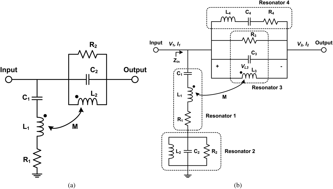
Figure 1(a) shows the first-order (two-resonator) lumped-element absorptive bandstop filter circuit topology. All design parameters of this topology are given in [Reference Lee, Lee and Chappell14] and are determined by the Q-factor of the resonators and the center frequency. This, in turn, means that the frequency response of this topology is set by the Q-factor of the resonators. One of the important characteristics of this topology is that a lower Q-factor results in a larger bandwidth. Hence, the resonators with a lower Q-factor needs to be employed to achieve a larger bandwidth. However, a lower Q-factor deteriorates the frequency selectivity. For achieving a different frequency response with a given Q-factor, this paper shows a rigorous methodology for extending to the second order. We will show that the second-order topology exhibits a larger bandwidth with a given Q-factor, or alternatively a better out-of-band response for a given isolation and bandwidth specification. The second-order (four-resonator) filter circuit topology is shown in Fig. 1(b). Similarly to the first-order (two-resonator) topology, it has mutual coupling between two inductors. It is worth noting that the methodology of expanding to a higher-order design for the absorptive bandstop filter is different from that for the reflective bandstop filter and the design equations have been obtained by deriving the expressions for S-parameters.

Fig. 1. Lumped-element absorptive bandstop filter topology. (a) First-order (two-resonator). (b) Second-order (four-resonator).
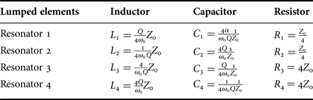
The lumped-element values can be determined using the fact that power transfer and reflection do not take place at the center frequency. The lumped element values of each resonator are summarized in Table 1 and the mutual coupling between inductors 1 and 3 is given by
 $$M=\displaystyle{2 \over Q}\sqrt {L_1\, L_3 }\comma \;$$
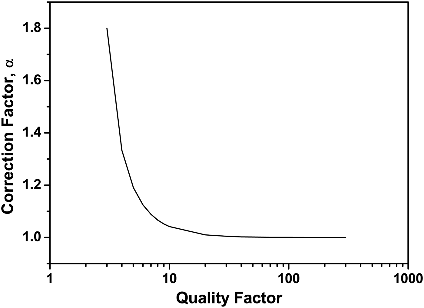
where Q is the Q-factor of the resonators. As in the first-order filter design, a correction factor, α, is introduced to compensate the frequency deviation of resonator 1 due to the inductive coupling. Using the fact that the magnitude of transmission and reflection coefficients of the absorptive bandstop filter is theoretically zero at the center frequency, the accurate value of the correction factor can be found by solving the equations for the transmission and reflection coefficients. The transmission and reflection coefficients have been derived and are given in Appendix. Figure 2 shows the correction factor as a function of the Q-factor of the resonators. According to (1), the mutual coupling between resonators 1 and 3 becomes smaller as the Q-factor increases. Therefore, the correction factor approaches unity for a large Q-factor.
Fig. 2. The relationship between the correction factor and the Q-factor.
Table 1. Lumped element values for the original prototype
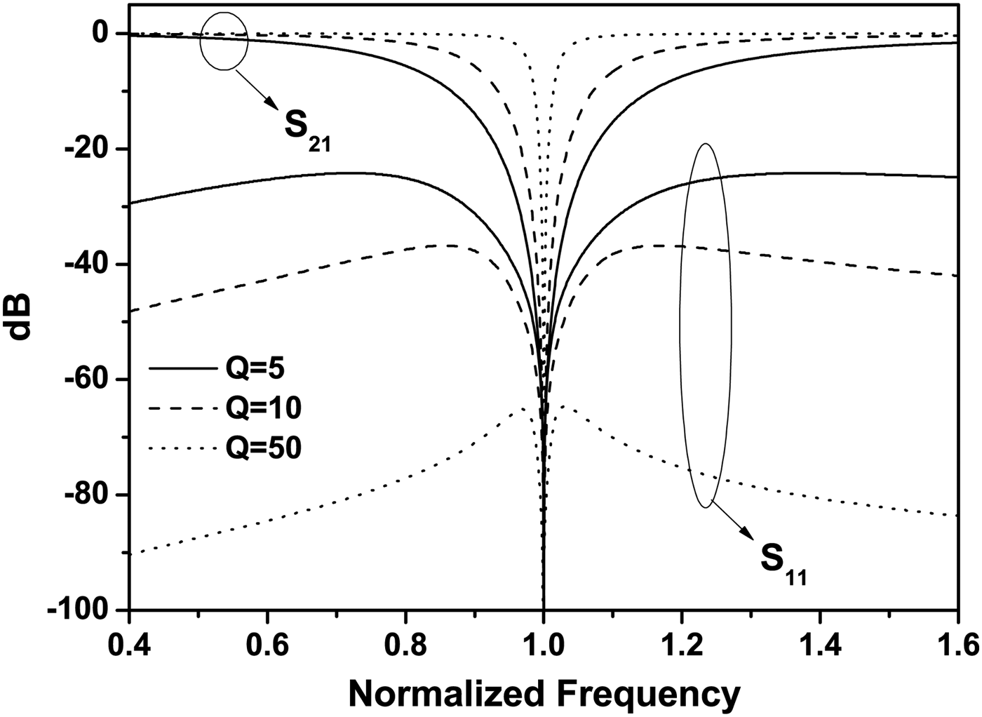
Figure 3 shows the frequency responses of the proposed second-order absorptive bandstop filter topology in the normalized frequency domain with different Q-factors. It can be seen that a bandstop filter with higher-Q resonators exhibits a narrower bandwidth. In addition, it is shown that the attenuation is infinite at the center frequency for all Q-factors and the impedance is perfectly matched at the center frequency. This verifies that the presented second-order filter topology exhibits the absorptive characteristic.
Fig. 3. The frequency responses of the second-order absorptive bandstop filter topology with different Q-factors.
Figure 4(a) compares the frequency response of the second-order absorptive bandstop filter with that of the first-order filter for the case that the Q-factor is 10. It is observed that the second-order filter exhibits a wider bandwidth. For example, 20 dB fractional bandwidths of the second-order and the first-order filters are 6.7 and 2.0%, respectively. This verifies that a higher-order filter can have a wider bandwidth. Figure 4(b) shows the case where an isolation is required for a given bandwidth as might be for a system specification. In this case the 20 dB specification is required for 6.7%. Q of 3.2 allows the first-order filter topology to have the same 20 dB bandwidth. It is shown that using the second-order filter topology is more attractive since it exhibits a better frequency selectivity having the same 20 dB bandwidth.
Fig. 4. Comparison between the first-order and the second-order bandstop filter topology. (a) Both responses are for Q = 10. (b) Q = 10 for the second-order filter topology. Q = 3.2 results in the same 20 dB bandwidth for the first-order filter topology.
B) Modified topology
We have shown that the proposed second-order bandstop filter topology exhibits the absorptive characteristic. The presented design equations in Table 1 are straight-forward and the lumped-element values can be obtained with ease. For example, the lumped-element values of a filter centered at 1 GHz whose resonator Q-factor is 5 can be determined, and they are L 1 = 9.947 nH, C 1 = 3.032 pF, R 1 = 12.5 Ω, L 2 = 0.398 nF, C 2 = 63.662 pF, R 2 = 12.5 Ω, L 3 = 6.366 nH, C 3 = 3.979 pF, R 3 = 200 Ω, L 4 = 159.155 nH, C 4 = 0.159 pF, and R 4 = 200 Ω. All these values are realizable theoretically, but some values are unrealistic in practice. For example, L 2 is too small and L 4 is too large to implement. Hence, we modify the presented topology shown in Fig. 1(b) in such a way that these values become realistic.
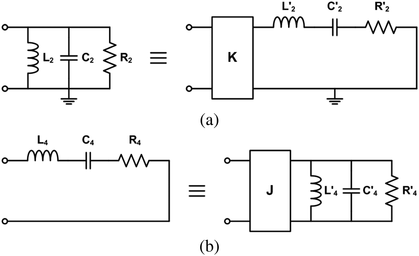
Since L 2 is too small, we convert the resonator 2 (parallel resonator) into a series resonator using an impedance inverter. Figure 5(a) shows an equivalent circuit of the parallel lumped-element resonator where K represents the impedance inverter. The lumped element values of the equivalent circuit are given by
Fig. 5. (a) Equivalent circuit of the parallel resonator. (b) Equivalent circuit of the series resonator.
 $$\eqalign{ & L^{\prime}_2=C_2\, K^2\comma \; \cr & C^{\prime}_2=\displaystyle{{L_2 } \over {K^2 }}\comma \; \cr & R^{\prime}_2=\displaystyle{{K^2 } \over {R_2 }}.}$$
In converting the parallel resonator into the series resonator, we are allowed to choose an arbitrary value for a series inductor. Hence, an inductor with a realistic value can be employed in filter design. Similarly, we can convert resonator 4 (series resonator) into a parallel resonator since L 4 is unrealistic. Figure 5(b) shows an equivalent circuit of the series lumped-element resonator where J represents an admittance inverter. The lumped element values of the equivalent circuit are given by
 $$\eqalign{ & L^{\prime}_4=\displaystyle{{C_4 } \over {J^2 }}\comma \; \cr & C^{\prime}_4=L_4\, J^2\comma \; \cr & R^{\prime}_4=\displaystyle{1 \over {R_4\, J^2 }}.}$$
Using the equivalency shown in Fig. 5, we can replace unrealistic inductors by realistic inductors, and realistic inductor values can be arbitrarily chosen in determining the inductor values for resonators 2 and 4. In the previous example, unrealistic inductors were L 2 = 0.398 nF and L 4 = 159.155 nH in the original prototype. These inductors can be removed by converting the series resonator into the parallel resonator and vice versa. Resonator 2 can be converted into a series resonator as shown in Fig. 5(a). In this example, L 2′ is arbitrarily chosen to be 3.4 nH. The other element values can be found from (2), and they are K = 7.308, C 2′ = 7.450 pF, and R 2′ = 4.273 Ω. Similarly, resonator 4 can be converted into a parallel resonator as shown in Fig. 5(b). L 4′ can be arbitrarily chosen. In this example, it is 3.4 nH and (3) leads to J = 6.842 × 10⁻³, C 4′ = 7.450 pF, and R 4′ = 106.814 Ω.
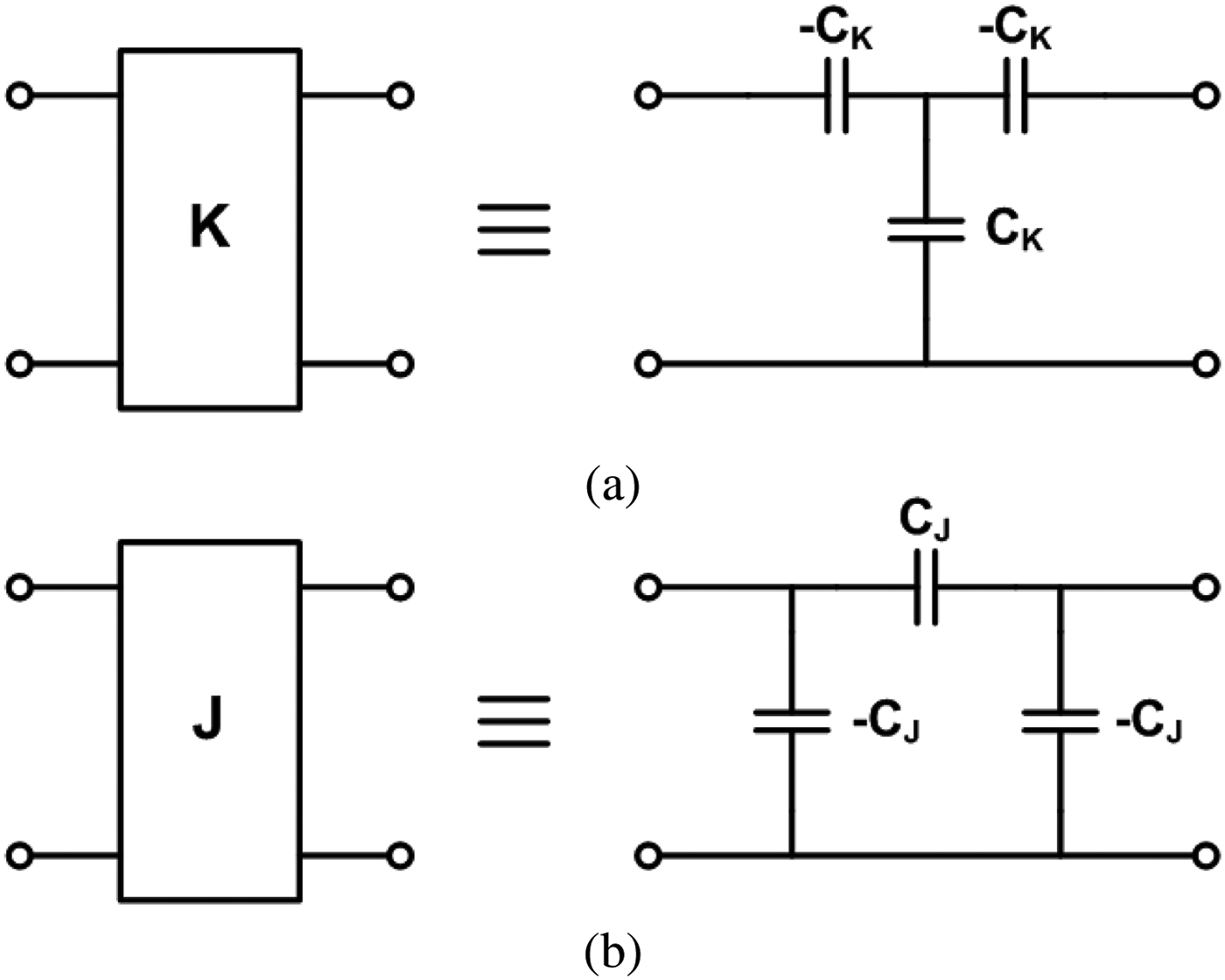
The impedance and admittance inverters can be implemented using capacitors. Figure 6 shows implementation of the impedance and admittance inverters, and the capacitor values are given by
 $$\eqalign{ & C_K=\displaystyle{1 \over {\omega _0\, K}}\comma \; \cr & C_J=\displaystyle{J \over {\omega _0 }}\comma \; }$$
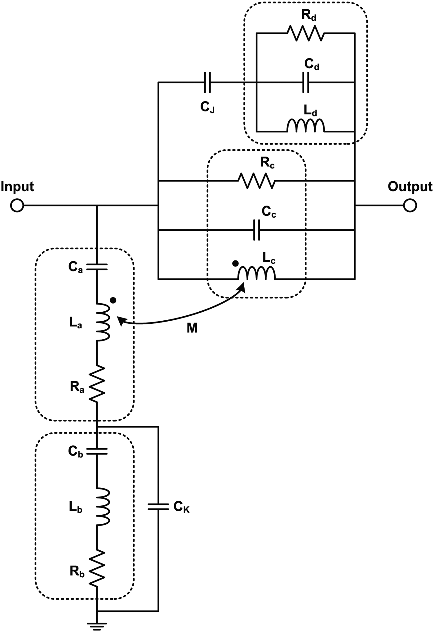
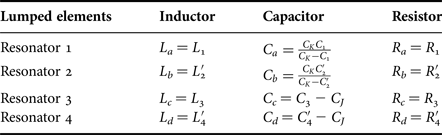
where ω 0 is the angular center frequency of the filter. Using the equivalent circuits of the resonators shown in Fig. 5 and the practical implementation method for the impedance and admittance inverters shown in Fig. 6, we can modify the original presented prototype (Fig. 1(b)) and the modified prototype is shown in Fig. 7. The lumped element values are summarized in Table 2. It is worth noting that the negative-valued capacitors are absorbed by neighboring capacitors.
Fig. 6. (a) Realization of the impedance inverter. (b) Realization of the admittance inverter.
Fig. 7. Modified second-order lumped-element absorptive bandstop filter topology.
Table 2. Lumped element values for the modified prototype
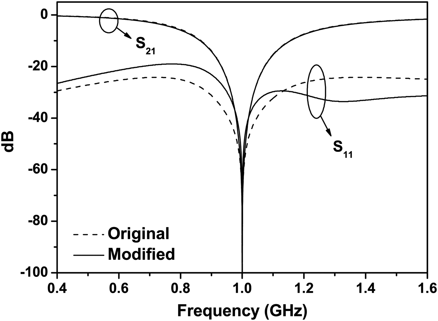
For verification of the modified topology, the frequency responses of two filters of the original and modified topologies have been compared. The center frequency of the filters and the resonator Q-factor are chosen to be 1 GHz and 5, respectively, for demonstration. Figure 8 shows the frequency responses of the filters. Two filter topologies show the identical response at the center frequency, which verifies the modified topology.
Fig. 8. Comparison between the original and the modified absorptive bandstop filter topology.
III. FABRICATION AND MEASUREMENTS
For verification of the proposed topology, a second-order absorptive bandstop filter has been designed, fabricated, and measured on low-temperature co-fired ceramic (LTCC).
The center frequency of the absorptive bandstop filter is 1 GHz, and the Q-factor of each resonator is designed to be 5. The design values of each component can be calculated from the equations we discussed in the previous section. The final design values in Fig. 7 are C a = 3.52 pF, C b = 11.3 pF, C c = 2.89 pF, C d = 6.36 pF, C K = 21.8 pF, C J = 1.09 pF, L a = 9.95 nH, L b = 3.4 nH, L c = 6.37 nH, L d = 3.4 nH, R a = 12.5 Ω, R b = 4.27 Ω, R c = 200 Ω, R d = 106.8 Ω, and M = 3.18 nH.
Since the inductors, L a and L c, need to have a specific mutual coupling inductance of M, the inductors are designed and simulated on multi-layer LTCC structure using Ansoft Designer which is a method-of-moment simulator. The three-dimensional (3D) view of the multi-layer inductors is shown in Fig. 9. The total number of the conductor layers and dielectric layers are 4 and 3, respectively. Inductor L a is on layer 1 (top layer) and inductor L c is on layer 3. The dielectric constant of the LTCC is 5.8 ± 0.2, and the loss tangent is 0.002. The thickness of first, second, and third dielectric layers are 150 µm, 150 µm, and 2 mm, respectively. Silver is printed with a thickness of about 0.5 mil, and gold plating is done on the top of the silver footprint. Based on the design rules for the LTCC structure, the diameter of each via-hole has been determined to be 150 µm, and that of each via-hole pad has been chosen to be 300 µm. The other dimensions of the mutually-coupled inductors can be determined observing the input impedance and admittance seen at one port of each inductor in the process of EM simulation, and they are shown in Fig. 10.
Fig. 9. 3D view of the customized on-chip inductor design. The dielectric constant of the LTCC is 5.8. h1 = 150 µm, h2 = 150 µm, and h3 = 2 mm.
Fig. 10. Top view of the customized on-chip inductor design. s1 = s3 = 175, w1 = w2 = w3 = 200, s_pad = 100, via = 150, via_pad = 300, Law = 1800, Lal = 1800, Lcw = 1600, Lcl = 1600, dx = 150, and dy = 250. All dimensions are in µm.
Commercially available surface mount devices (SMDs) are used for the other lumped elements. To minimize the effect of the transmission lines and the total area of the filter for given minimum Q-factors, 0604-sized SMD inductors, 0402-sized SMD varactors, and 0201-size SMD resistors are used as shown in Fig. 11(a). The varactors are utilized to give a flexibility of capacitances to compensate the tolerance of each lumped-element component. Each capacitor is implemented by two varactors whose cathodes are connected to each other. DC power is supplied to the cathodes via a resistor R dc. The resistors, R dc, in Fig. 11(a) are all 10 kΩ and used as RF chokes to bias varactors properly. EM simulation for the entire structure has been carried out using Agilent ADS. The SMD components have been soldered on the top layer of the LTCC structure. The photograph of the fabricated filter is shown in Fig. 11(b). The total area of the LTCC is 6.2 mm by 19.3 mm, and the total area of the filter excluding outer ground ring, GSG pads, and DC pads for the measurement is 4 mm by 12.2 mm.
Fig. 11. Top view of the entire filter design. (a) Layout of the entire filter with SMD arrangements corresponding to Fig. 7. 0604-sized SMD inductors, 0402-sized SMD varactors, and 0201-sized SMD resistors are used. (b) A photograph of the fabricated bandstop filter after assembling SMDs. The total area of the LTCC is 6.2 mm by 19.3 mm, and the total area of the filter excluding outer ground ring, GSG pads, and DC pads for the measurement is 4 mm by 12.2 mm.
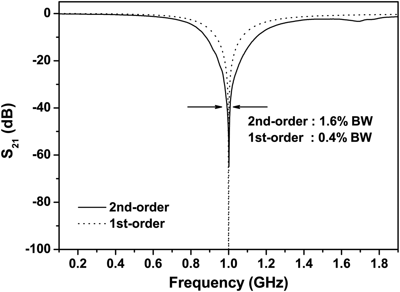
Cascade 350 µm-pitch GSG RF probe has been used in measurement. For measurement, the 50 Ω CPWG lines have been designed for both input and output ports. An Agilent N5230C PNA-L Network Analyzer has been used for S-parameter measurements. The S-parameters with a comparison between measured and simulated responses are shown in Fig. 12. The measured and simulated insertion losses at 0.6 GHz are 1.24 and 1.39 dB, respectively, and those at 1.4 GHz are 2.68 dB and 3.04 dB, respectively. The measured and simulated 20 dB bandwidth are 12.0 and 14.7%, respectively. It is shown that the measured and simulated responses agree well. In addition, both measured and simulated transmission coefficient shows attenuation larger than 50 dB at the center frequency. A small discrepancy in the reflection coefficients is mainly attributed to the parasitics of LTCC structure and SMD components. Comparison between the second-order and first-order absorptive bandstop filter is shown in Fig. 13. It is shown that the proposed second-order filter topology exhibits a larger bandwidth with the absorptive characteristic, which is the benefit of using the proposed topology. For example, the measured 40 dB bandwidth of the second-order filter is 1.6% and the theoretical 40 dB bandwidth of the first-order filter is only 0.4%. In other words, the first-order filter has a small stopband and it can suppress only a frequency band of 0.4% with 40 dB attenuation. This comparison indicates that the second-order filter is more useful in blocking transmission from neighboring bands.

Fig. 12. Measured and simulated responses of the second-order lumped-element absorptive bandstop filter.
Fig. 13. Comparison between the measured response of the second-order absorptive bandstop filter and the theoretical response of the first-order filter. Two filters have the same Q-factor (Q = 5) for comparison.
IV. CONCLUSION
This paper has proposed a new lumped-element absorptive bandstop filter topology containing four resonators. This topology exhibits a wider bandwidth compared to the topology containing two resonators. We also have shown a methodology for avoiding the use of impractical lumped elements. For this purpose, the inverter concept has been adopted in converting a series resonator into a parallel resonator and vice versa while maintaining the critical relationship for the absorptive filter. For verification of the proposed topology, we have designed and fabricated a lumped-element bandstop filter. Two inductors which are required to have mutual inductance have been fabricated in an LTCC structure. The measured results have shown that the new topology exhibits the absorptive characteristic with a wider bandwidth.
ACKNOWLEDGEMENTS
This work was supported by the Basic Science Research Program through the National Research Foundation of Korea (NRF) funded by the Ministry of Education, Science, and Technology (grant no. NRF-2012R1A1A1004665).
Appendix
In this section, we provide the expressions for the transmission and reflection coefficient of the proposed topology shown in Fig. 1(b). The derivation starts with defining node voltage V 1 and current I 1 at the input port and V 2 and I 2 at the output port where the output port is terminated by Z 0. Using the circuit theory, the input impedance, Z in, is given by
 $$Z_{in}=\displaystyle{{V_1 } \over {I_1 }}.$$
The reflection coefficient, S 11, can be derived by
 $$S_{11}=\displaystyle{{Z_{in} - Z_0 } \over {Z_{in}+Z_0 }}.$$
The transmission coefficient, S 21, can also be calculated by
 $$\eqalign{ & V_1=V_1^++ V_1^ -\comma \; \cr & V_2=V_1 - V_{L3}=I_2^ - Z_0=V_2^ - .}$$
As a result, the expressions for the coefficients can be obtained and they are
 $$\eqalign{ & S_{11}=\displaystyle{{e_1\, s+e_0 } \over {f_1\, s+f_0 }}\comma \; \cr & S_{21}=2 \cdot \displaystyle{{g_1\, s+g_0 } \over {f_1\, s+f_0 }}\comma \; }$$
where
 $$\eqalign{e_1 & =PZ_4 Y_2 M+Z_4 Y_2\, L_1 - PZ_0 Z_4 Y_2 Y_3\, L_3 \cr & \quad - PZ_0 Y_2\, L_3 - Z_0 Z_4 Y_2 Y_3 M - Z_0 Y_2 M\comma \; \cr e_0 & =Z_1 Z_4 Y_2+Z_4 - Z_0 Z_4 Y_2 - PZ_0 Z_4 Y_2\comma \; \cr f_1 & =PZ_4 Y_2 M+Z_4 Y_2\, L_1+PZ_0 Z_4 Y_2 Y_3\, L_3 \cr & \quad +PZ_0 Y_2\, L_3+Z_0 Z_4 Y_2 Y_3 M+Z_0 Y_2 M\comma \; \cr f_0 & =Z_1 Z_4 Y_2+Z_4+Z_0 Z_4 Y_2+PZ_0 Z_4 Y_2\comma \; \cr g_1 & =PZ_0 Z_4 Y_2 Y_3\, L_3+PZ_0 Y_2\, L_3+Z_0 Z_4 Y_2 Y_3 M+Z_0 Y_2 M\comma \; \cr g_0 & =PZ_0 Z_4 Y_2 .}$$
In the above equations, Z 1, Y 2, Y 3, and Z 4 are given by
 $$\eqalign{Z_1 & =R_1+\displaystyle{1 \over {sC_1 }}\comma \; \cr Y_2 & =sC_2+\displaystyle{1 \over {R_2 }}+\displaystyle{1 \over {sL_2 }}\comma \; \cr Y_3 & =sC_3+\displaystyle{1 \over {R_3 }}\comma \; \cr Z_4 & =R_4+sL_4+\displaystyle{1 \over {sC_4 }}\comma}$$
and P is given by
 $$P=\displaystyle{{q_1\, s+q_0 } \over {r_1\, s+r_0 }}\comma$$
where
 $$\eqalign{ & q_1=Z_4 Y_2\, L_1 - Z_4 Y_2 M - Z_0 Z_4 Y_2 Y_3 M - Z_0 Y_2 M\comma \; \cr & q_0=Z_1 Z_4 Y_2+Z_4\comma \; \cr & r_1=Z_4 Y_2\, L_3+Z_0 Z_4 Y_2 Y_3\, L_3+Z_0 Y_2\, L_3 - Z_4 Y_2 M\comma \; \cr & r_0=Z_0 Z_4 Y_2 .}$$
  Juseop Lee received his B.E. and M.E. degrees in Radio Science and Engineering from Korea University, Seoul, Korea, in 1997 and 1999, respectively, and Ph.D. degree in Electrical Engineering from The University of Michigan, Ann Arbor, MI, USA, in 2009. In 2001, he joined Electronics and Telecommunications Research Institute (ETRI), Daejeon, Korea, where he was involved in the design of passive microwave equipment for Ku- and Ka-band communications satellites. In 2009, he joined Purdue University, West Lafayette, IN, USA, where he was a Post-Doctoral Research Associate, during which time his activities included the design of adaptable RF systems and invention of field-programmable filter arrays (FPFAs). In 2012, he joined Korea University Seoul, Korea, where he is currently Associate Professor. His research interests include reconfigurable RF and microwave components, satellite transponders, and wireless power transfer.
 Byungguk Kim received his B.S. degree in Electrical and Electronic Engineering from Ajou University, Suwon, South Korea and B.E. degree in Electrical and Computer Engineering from Stony Brook University, Stony Brook, New York in 2007. He also received his M.S. and Ph.D. degrees in Electrical and Computer Engineering from Purdue University, West Lafayette, Indiana, in 2014. His research interests are RF powering circuits for remote power sensors and lumped-element tunable absorptive bandstop filters using low-Q resonators.
 Kangho Lee received his B.S. degree in Computer and Communications Engineering from Korea University, Seoul, Korea, in 2013. He is currently working toward M.S. degree in Radio Communications Engineering at Korea University. He has been involved in research programs supported by Agency for Defense Development, National Research Foundation, and Electronics and Telecommunications Research Institute. His current research focuses on microwave passive devices, especially substrate-integrated waveguide filters using tunable resonators.
 William J. Chappell received his B.S.E.E., M.S.E.E., and Ph.D. degrees from The University of Michigan at Ann Arbor, Ann Arbor, MI, USA, in 1998, 2000, and 2002, respectively. He is a Program Manager in the Microsystems Technology Office (MTO), Defense Advanced Research Projects Agency (DARPA), Arlington, VA, USA. He is on a temporary assignment at DARPA as an IPA from his home institution of Purdue University, West Lafayette, IN, USA. At DARPA, he is the Program Manager of the Adaptive RF Technologies (ART) program and the Arrays at Commercial Timescales (ACT) program. While at Purdue, he leads the IDEAS lab focusing on applied electromagnetic for sensors and communications.