


Introduction
Oscillators with the role of producing a stable signal source and pure spectrum at a desired frequency are used in communication systems. The performance of an oscillator depends on resonators with high-quality factor (Q). In planar resonator, the quality factor is not more than a few hundreds and when placed in the feedback of oscillator, the quality factor further decreased. It is not possible to increase their quality factor to be comparable with non-planar resonators. Among different types of resonators, dielectric resonator (DR) due to low losses, temperature stability, and ability of excellent integrality with RFIC is the best choice to use as a frequency determining element in the feedback loop of oscillators [Reference Li, Liu and Bao1–Reference Hady, Kishk and Kajfez3]. Recent DRs operating in the TE 01δ, commonly resonant mode in cylindrical DRs which most of the stored electric energy is located in the cylinder. The remaining energy is distributed out of the cylinder in the air around the resonator, decaying with distance from the resonator surface. They perform quality factor between 10 000 and 30 000 at 10 GHz. Owing to their high-quality factor, they are used in low phase noise oscillators. Moreover, to integrate a resonator in a circuit, the efficient coupling between the resonator and the transistor is essential. Loaded Q in the resonators affected by specification of coupled lines is the determining factor in measuring phase noise. Recently, several attempts have been made to design and implementation of DR oscillators (DROs) with minimum phase noise [Reference Plourde and Ren4–Reference Kajfez and Guillon6]. For the first time, Cohn reported that by using an elliptical filter as a resonator, the loaded quality factor will be increased and phase noise will be decreased [Reference Cohn7]. However, the filter's quality factor is still limited by the unloaded quality factor of their constituent resonators which are limited due to the dielectric, conductor, and radiation losses. Another way of compensating for the energy losses of a passive resonator is coupling negative resistance to the resonator. Significant phase noise reduction is achieved by designing an active resonator or adding negative resistance in resonators to enhance their unloaded quality factors [Reference Chang and Itoh8–Reference Nick11]. Appropriate choice of the transistor and coupling shows that the equivalent resistance of the resonator can be canceled by produced negative resistance in an active feedback loop. Moreover, using high-quality factor active filter at its transmission zeros in the oscillator is another phase noise reduction technique [Reference Choi, Nick and Mortazawi12, Reference Lee, Lee and Nam13]. The frequency response of DR filters in active feedback indicates that unloaded quality factor will be increased [Reference Madrangeas, Jarry, Guillon, Larroque, Theron and Parise14]. Active resonators due to their high loaded quality factor are appropriate to design oscillator with low phase noise [Reference Lee, Lee and Nam15, Reference Chen, Hong, Chen, Zhou and Sheng Li16]. However, they can add extra noise sources which have negative effects on the oscillator phase noise. Therefore, oscillator performance can be improved if the effect of extra noise source added to the circuit is minimized. In addition, the power consumption of oscillators with active resonator due to the existence of two active devices will be more than passive ones. Spurious oscillation in the active loop is another problem that should be prevented. To overcome these drawbacks, a new structure of DROs with active resonator employing a single transistor is proposed in this work. It can be used in low phase noise application by increasing loaded quality factor. The basis of this idea is to utilize a single active device to achieve two goals, oscillation and activation of DR. An interesting feature of this oscillator is the simplicity in the structure. Negative resistance added to DR through additional TL and added coupled lines are determined by the amount of the gain injected from the single transistor which makes the circuit oscillate. There is no need to use two active devices and consume extra power supply, thereby obtaining significant improvement in phase noise performance. Oscillation only occurs at the resonance frequency of DR and spurious frequency is prevented. Although this approach has been performed for DR oscillator, it can be used in oscillators with various resonators. The proposed method will be compared with a passive DRO at 8 GHz by simulation and experimental results to show the effect of adding active feedback.
Quality factor optimization
Phase noise theory
The unloaded Q is a critical factor on the phase noise because it is affected by the conductor and dielectric losses. Also, choosing the type of resonator and coupling to the amplifier is important. Phase noise is represented by Leeson's formula. According to equation (1), I.L is the insertion loss of the resonator, F is the noise figure of the amplifier, K is Boltzmann constant, T is ambient temperature, Q L is the loaded quality factor of the resonator, Δω is the frequency offset from the carrier, and ω c is the flicker-noise corner frequency where flicker and white noise components are equal.
In oscillators, phase noise is proportional to the inverse-square of the resonators' loaded Q [Reference Leeson17]. Furthermore, increasing the resonator's insertion loss, I.L, degrade the phase noise. Therefore, to reduce the phase noise of an oscillator, it is necessary to increase the loaded Q. In other words, resonators and coupling structure should be designed to achieve this goal.
 $$L{\rm (}f\,{\rm )} = \displaystyle{{FKTB\,I.L.} \over {2P_0}}\left[ {1 + {\left( {\displaystyle{{\omega_0} \over {2Q_L\Delta \omega}}} \right)}^2} \right]\left( {1 + \displaystyle{{\omega_c} \over {\Delta \omega}}} \right).$$
Design and implementation of active resonator
Adding an active feedback or coupling a negative resistance to the resonator is the solution for the reduction of the oscillator's phase noise. By using a resonator in the active feedback loop, Q L can be increased [Reference Chen, Hong, Chen, Zhou and Sheng Li16]. Figure 1 illustrates the structure of conventional active resonator oscillator. Gap distances, g 1 and g 2 between the resonator and second amplifier, can be modeled by transformer ratios n 1 and n 2 which determines the amounts of coupling between resonator and amplifier. To fully compensate for the losses of the resonator, unloaded Q (Q u) is infinite. Q 1 and Q 2, quality factors of input and output loading of passive resonator coupled to active feedback are defined as follows [Reference Chen, Hong, Chen, Zhou and Sheng Li16] which L r is the inductance and R r is the resistance of DR equivalent circuit:
 $$\eqalign{& Q_1 = \left( {\displaystyle{{50n_1^2} \over {L_r\omega_0}}} \right) \cr & Q_2 = \left( {\displaystyle{{50n_2^2} \over {L_r\omega_0}}} \right) \cr & Q_u = \left( {\displaystyle{{R_r^{}} \over {L_r\omega_0}}} \right).} $$
Fig. 1. Circuit schematic of conventional active resonator oscillator proposed in [Reference Nick and Mortazawi10].
Eventually, the loaded quality factor will be obtained as:
 $$\eqalign{& Q_1 = \left( {\displaystyle{{G_{}^2 -1} \over {G^2}}} \right)Q_u \cr & Q_2 = \lpar {G^2-1} \rpar Q_u.} $$
It should be noted that G in equation (3) is the gain of the second amplifier compensating for the losses in the resonator. Noise is added to the oscillator and more power is consumed by using an additional transistor. Consequently, stability will be degraded and DC-to-RF efficiency will be decreased. In addition, spurious oscillation may occur if the condition of starting oscillation is satisfied in an additional feedback loop.
Single transistor active resonator oscillator
To suppress the aforementioned problems, instead of using an additional transistor in feedback loop, a new structure of active resonator oscillator using a single active device is presented. The principle of this method is increasing loaded Q of resonator via the single transistor in oscillator structure by an extra coupling in feedback loop. By this feedback loop, enough gain is injected to the resonator to compensate the losses. Therefore, according to equation (3), loaded Q will be increased and consequently phase noise will be reduced. Compared with a conventional active resonator oscillator, no extra noise sources due to additional transistor will be added. In addition, power consumption will be reduced which leads to enhance DC-to-RF efficiency.
Figure 2 presents a block diagram of the proposed structure of active DRO with a single active device. The difference between the proposed DRO and a passive DRO is the existence of two coupled lines and middle TL. The spacing of coupled lines, g 1 and g 2 determine the amount of coupling gain to the resonator. G, gain of transistor must be chosen carefully to meet the oscillation condition. Coefficients n 1 and n 2 can be determined by equation (2) for specific Q. Therefore, the dimension of coupled lines can be synthesized with Ansoft HFSS software. The length of middle TL is a critical parameter on which the amount of loaded quality factor depends. By adjusting the length of this line, the reactance of the equivalent circuit will be altered. The optimized value shall be used to find minimum phase noise. The gain in equation (3) is equal to the ratio of measured voltages around coupled lines. It should be noted that the amplifier is bilaterally conjugate matched at the input and output.

Fig. 2. Simple model of DRO with a proposed active resonator.
In coupled DR, by changing the distance between DR and two microstrip TLs, the ratio between Q 0 and Q L can be altered. It can be modeled as shown in Fig. 3. R, L, C defines the resonator equivalent impedance Z.

Fig. 3. Equivalent circuit model of double-coupled dielectric resonator.
The R determines the losses in the DR, β 1 and β 2are the resonator's input and output external couplings. The input and output coupling are related together by loaded quality factor and insertion loss as shown in equation (4) [Reference Khanna and Garault18, Reference Soares, Graffeuil and Obregon19]:
 $$\eqalign{& Q_L = \displaystyle{{Q_0^{}} \over {1 + \beta _1 + \beta _2}} \cr & I.L = 20\log \displaystyle{{1 + \beta _1 + \beta _2} \over {2\sqrt {\beta _1\beta _2}}}.} $$
Consequently, the equivalent circuit of the proposed DRO in Fig. 2 can be shown as Fig. 4. As a result of considering the equal distance between TLs and DR, β 1 and β 2 have the same value and are equal to β 0. Q L represents the effects of loading on input and output of resonator. Extra coupling from transistor to resonator is created via transformers with coupling coefficients n 1 and n 2. Middle TL is modeled by a transformer of β c. Gain amplitude in the second feedback is not enough to build oscillation and only the phase condition is satisfied. Phase condition guarantees that the frequency of oscillation will not be shifted by adding extra feedback. Ratios of n 1 and n 2 determine the amount of gain injected to the resonator.

Fig. 4. Equivalent circuit of oscillator with a proposed active dielectric resonator.
Oscillator design
The configuration of a practical proposed oscillator with active DR is shown in Fig. 5. It consists of low noise amplifier, phase shifter, output coupler, and high Q resonator with active feedback. The oscillator components are realized using microstrip TL on Rogers RO4003C substrate. The procedure of designing is summarized in this section, each part is designed and implemented separately.

Fig. 5. Block diagram of oscillator with a proposed active dielectric resonator.
Amplifier
To design the microwave oscillator, the nonlinear model for the transistor must be used. Therefore, the Gunmel-Poon model of transistor with a parasitic element is chosen. The gain of the selected amplifier must be enough to compensate for the insertion loss of additional coupler in the feedback loop, resonator, phase shifter, output coupler, connectors, and cables. When the oscillator is initially switched on, the gain of the amplifier must be sufficient to provide a loop gain greater than unity. Infineon BFP520F, high gain, and low noise SiGe bipolar transistor are chosen as an active device. It is biased at V CE of 2.0 V and I C of 36 mA. The overall effect of the bias T is to isolate DC from RF. In the biased circuit, the radial stub and TLs have an electrical length of 90° at 8 GHz to ensure that the network will be open circuit at high frequencies. A 4.5 V dc voltage is used to supply the amplifier. The measurements are performed using the HP 8720B and network analyzer. Figure 6(a) shows the DC bias circuit used for amplifier and also the realized amplifier is depicted in Fig. 6(b).

Fig. 6. (a) DC bias circuit (b) Fabricated experimental prototype of the amplifier.
The measured frequency response of biased transistor in Fig. 7 shows 7.7 dB gain at 7.99 GHz. The significant low-frequency gain should be noted. To reduce its effect and ensure the stability, two resistances in series with bias T connected to base and collector are implemented.

Fig. 7. Measurement results of the designed amplifier.
The DR
The stability and spectral purity of the oscillator signal depend on the characteristics of the resonator. The unloaded Q of the resonator is dependent on material properties and therefore depends on the type of the selected resonator. High unloaded Q cannot ensure that DRO will carry out a good response with low phase noise. Given that, loaded Q performs an important role in designing circuits, choosing DR and appropriate coupling to the circuit are essential. In this work, a pair of microstrip TLs were used to couple power to DR as a bandpass structure. Without spacer, the magnetic field of puck dissipates in the ground plane. Therefore, the puck is mounted into a spacer with a height equal to H s mounted onto the PCB. This oscillator uses a Barium Zinc Tantalate (BaZnTaO3) DR puck with ε r equal to 29.5 ± 1, the diameter is 7.8 mm, and the height H d is 3.2 mm. The resonance frequency is 7.9914 GHz and Q 0 is equal to 9000(@10 GHz). The length of the coupled TLs and distance between them are important due to their effect on the value of loaded Q. The coupling coefficient is maximum when the puck is placed at a distance of a quarter-wavelength from the end of a pair of open circuit lines. By changing the distance between the DR and the two microstrip lines, the ratio between the unloaded quality factor Q 0 and the loaded quality factor Q L can be varied. Obtaining the proper gap size is necessary to provide the desired coupling of the resonator.
Calculating quality factor and resonant frequency by numerical method
The DR acts as a magnetic dipole. So, the voltage inducted in a microstrip line through the current in the DR can be calculated from the magnetic flux in the cross-section of the microstrip line [Reference Kajfez and Guillon6]:
 $$e_r = \int E{\rm \;}. {\rm \;\;} dl = j\omega \mu _0\mathop \int \limits_s^{} H{\rm \;}. {\rm \;} dS.$$
Therefore, the external quality factor, which is a function of the distance between the microstrip line and the resonator as well as the length of the line, is given by
 $$Q_e = \displaystyle{{4Z_c} \over {\omega _{0{\rm \; \; \;}} \mu _0^{2{\rm \;}} {\rm \;}}} {\rm \;} \displaystyle{{{\bar{w}}_m} \over {{\left[ {\mathop {\rm \int\!\!\!\int} \nolimits_s^{} H.dS} \right]}^2}},$$
with
 $$W_m = \displaystyle{1 \over {4{\rm \;}}} {\rm \;} \int \varepsilon _0\varepsilon _iE_iE_i^{\rm {^\ast}} d\tau _i,$$
ε i is the relative dielectric permittivity and E i the electric field in the medium with ε i. Also, the different quality factors, i.e. unloaded (Q 0), loaded (Q L), and external (Q e) quality factor are related together as:
 $$\displaystyle{1 \over {Q_L}} = \displaystyle{1 \over {Q_0}} + \displaystyle{1 \over {Q_e}}.$$
Therefore, to calculate quality factor, we need to know all electrical and magnetic fields in the shielding box. So, it is necessary to solve the Maxwell equation to calculate fields.
Since the structure of the DR is non-homogenous, consisting of different media (puck, spacer, substrate, and air), its numerical analysis will be challenging while requiring high accuracy. Based on the approximate approach used in [Reference Et, Rousset, Guillon and Garault20] to determine the resonance frequency through the FDM, the Helmotz equation in spherical coordinates for a cylindrical DR can be expressed as:
 $$\displaystyle{{\partial ^2\psi} \over {{\rm \;} \partial r^2}} + \displaystyle{1 \over r}\displaystyle{{\partial \psi} \over {\partial r}} + \left( {\omega^2\varepsilon \mu -\displaystyle{1 \over {r^2}}} \right)\psi + \displaystyle{{\partial ^2\psi} \over {\partial z^2}} = 0.$$
This equation can be applied to both TE and TM modes, with φ = E z for TM modes and φ = H z for TE modes. The fields of the DR outside the puck are decreasing exponentially. Due to the rotational symmetry of the structure, cos (mϕ) and sin (mϕ) terms can be factored out from the Helmotz equation. Also, because of the biaxial symmetry on the two axes, only one-quarter of the cross-section needs to be considered. Figure 8 shows the parts of DR that is applied in Helmotz equation. At the interface between different media, the dirichlet condition for the TM modes and the Neumann condition for the TE modes should be considered.

Fig. 8. Composite dielectric structure.
- At the interface parallel to z between two different media:
 $$\left( {\displaystyle{{\partial E_\varphi} \over {\partial r}}} \right)_1 = \left( {\displaystyle{{\partial E_\varphi} \over {\partial r}}} \right)_2\,{\rm for\ TE\ Modes,}$$
 $$\displaystyle{1 \over {\varepsilon _{r1}}}\left( {\displaystyle{1 \over r}H_\varphi + \displaystyle{{\partial H_\varphi} \over {\partial r}}} \right)_1 = \displaystyle{1 \over {\varepsilon _{r2}}}\left( {\displaystyle{1 \over r}H_\varphi + \displaystyle{{\partial H_\varphi} \over {\partial r}}} \right)_2\,{\rm for\ TM\ Mode}{\rm.} $$
At the interface parallel to r between two different media:
 $$\left( {\displaystyle{{\partial E_\varphi} \over {\partial Z}}} \right)_1 = \left( {\displaystyle{{\partial E_\varphi} \over {\partial Z}}} \right)_2\,{\rm for\ TE\ Modes}$$
 $$\displaystyle{1 \over {\varepsilon _{r1}}}\left( {\displaystyle{{\partial H_\varphi} \over {\partial Z}}} \right)_1 = \displaystyle{1 \over {\varepsilon _{r2}}}\left( {\displaystyle{{\partial H_\varphi} \over {\partial Z}}} \right)_2\,{\rm for\ TM\ Modes}{\rm.} $$
By applying the integral form of the Maxwell equation to equation (11), we obtain:
 $$\eqalign{& \displaystyle{{\psi _{i + 1,j} + \psi _{i-1,j}-2\psi _{i,j}} \over {{({\rm \Delta} r)}^2}} + \displaystyle{{\psi _{i + 1,j}-\psi _{i-1,j}} \over {2r{\rm \Delta} r}} + \left( {\omega^2\varepsilon \mu -\displaystyle{1 \over {r^2}}} \right)\psi _{i,j} \cr & \quad \quad \quad \quad \quad \quad \quad \quad + \displaystyle{{\psi _{i,j + 1} + \psi _{i,j-1}-2\psi _{i,j}} \over {\lpar {{\rm \Delta} z^2} \rpar }} = 0.} $$
Then, by considering r = i.Δr and R = (Δr/Δz)2, the ratio between the mesh sizes in the r and z dimensions, we have:
 $$\eqalign{& \omega ^2\varepsilon _0\mu _0(\Delta r)^2\psi _{i,j} = \psi _{i,j}\displaystyle{1 \over {\varepsilon _r}}\left\{ {\displaystyle{1 \over {i^2}} + 2R^2 + 2} \right\}-\psi _{i + 1,j}\displaystyle{1 \over {\varepsilon _r}}\left( {\displaystyle{{2i + 1} \over {2i}}} \right) \cr & \quad \quad \quad \quad \quad \quad \quad -\psi _{i-1,j}\displaystyle{1 \over {\varepsilon _r}}\left( {\displaystyle{{2i-1} \over {2i}}} \right)-\psi _{i,j + 1}\displaystyle{{R^2} \over {\varepsilon _r}}-\psi _{i,j-1}\displaystyle{{R^2} \over {\varepsilon _r}}.} $$
This equation is valid for any node in the shielding box. Note that during the numerical analysis, the dielectric constant in the relation should be updated in each considered cell due to the different dielectric media involved. Also, at the different existing interfaces (substrate-spacer-air, puck-spacer-air, puck-air, and substrate-air), the dielectric constant value was averaged based on the dielectric constants of the corresponding media around a given point belonging to an interface. For illustration, let us consider a point at the interface of four different dielectric constant media as shown in Fig. 9.

Fig. 9. Node at the interface of four different dielectric media.
The related modified finite difference equation can be stated as:
 $$\eqalign{ \omega ^2\mu _0\varepsilon _0\psi _{{\rm i},{\rm j}} &= \left( {\displaystyle{1 \over {i^2}} + 2R^2 + 2} \right)\left( {\displaystyle{4 \over {\varepsilon_1 + \varepsilon_2 + \varepsilon_3 + \varepsilon_4}}} \right){\rm \;} \psi _{{\rm i},{\rm j}} \cr & \quad + \left( {1 + \displaystyle{1 \over {2i}}} \right)\displaystyle{{2\lpar {\varepsilon_1 + \varepsilon_4} \rpar } \over {\varepsilon _1 + \varepsilon _2 + \varepsilon _3 + \varepsilon _4}}{\rm \;} \psi _{{\rm i} + 1,{\rm j}} \cr & \quad + {\rm \;} \left( {1-\displaystyle{1 \over {2i}}} \right)\displaystyle{{2\lpar {\varepsilon_2 + \varepsilon_3} \rpar } \over {\varepsilon _1 + \varepsilon _2 + \varepsilon _3 + \varepsilon _4}}{\rm \;} \psi _{{\rm i}-1,{\rm j}} \cr & \quad + \displaystyle{{2\lpar {\varepsilon_3 + \varepsilon_4} \rpar R^2} \over {\varepsilon _1 + \varepsilon _2 + \varepsilon _3 + \varepsilon _4}}{\rm \;} \psi _{{\rm i}.{\rm j}-1} \cr & \quad + \displaystyle{{2\lpar {\varepsilon_1 + \varepsilon_2} \rpar R^2} \over {\varepsilon _1 + \varepsilon _2 + \varepsilon _3 + \varepsilon _4}}.} $$
For each node (i, j) in equation (14), an Eigenvalue problem is set and should be solved. By determining the eigenvalue λ = R 2ω 02ε 0μ 0 of the linear system, the DR resonance frequency can be achieved using equation (15) where Φ is eigenvalue function and A is multiplier matrix.
 $$A\Phi {\rm} = {\rm} \lambda \Phi {\rm} = {\rm} R^2\omega _0^2 \varepsilon _0\mu _0\Phi. $$
From each eigenvalue, we can achieve the resultant electric field in the ϕ direction, thus the remaining components of the EM field at any point of the structure through the Maxwell equations. Note that in order to apply the described method, the whole domain, i.e. the DR in the shielding box, was discretized with different mesh sizes. Outside the puck, because the fields are decreasing exponentially, the mesh sizes in the z dimension were doubled to decrease the computation time, so the value of R in equation (15) has doubled. By applying the finite difference method and solving the eigenvalue problem, the resonant frequency and loaded quality factor can be obtained.
Unwanted frequency rejection
The DR is placed in a metal cavity which performs different resonance frequency at different modes (a combination of m, n, p). Equation (16) illustrates the relation between resonance frequency (f r), dimension of cavity a, b, c, and a number of modes. In addition, to avoid unwanted oscillation in the resonance frequency of the metal cavity (box of DR) in Fig. 10, which are computed by equation (16) to happen at 2.3, 4.4, and 7.8 GHz, a piece of absorption material is attached on the interior side of the box [Reference Et, Rousset, Guillon and Garault20]. This helps suppress the related modes of excitation. Therefore, the unloaded quality factor will be decreased from 9600 to 8100.
 $$f_r = c\sqrt {{\left( {\displaystyle{m \over {2a}}} \right)}^2 + {\left( {\displaystyle{n \over {2b}}} \right)}^2 + {\left( {\displaystyle{\,p \over {2c}}} \right)}^2} \;. $$
Figure 11 depicts a photo of the fabricated resonator. After attaching absorption material, it has been used as a resonator in this measurement.

Fig. 10. The structure of the metal cavity of DR.
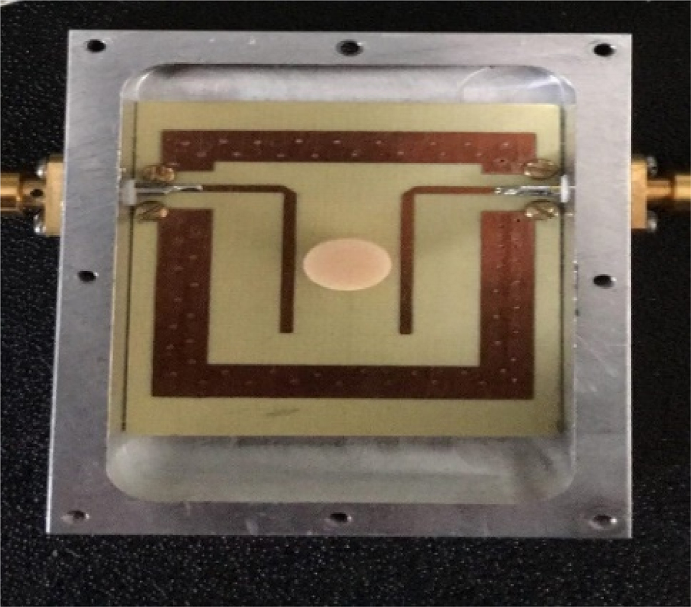
Fig. 11. Fabricated resonator in an aluminum box.
Numerical and measurement result of DR design
The effect of the microstrip line length on Q L is illustrated in Fig. 12. By varying the microstrip line length from 8 to 12 mm, the results show that by increasing the length of the microstrip line to half wavelength, the loaded quality factor increased and the resonance frequency decreased.

Fig. 12. (a) Loaded Quality Factor versus Transmission line length coupled to DR, (b) Resonance Frequency versus Transmission line length coupled to DR.
Figure 13 illustrates the dependency of the Q L on the distance between TLs as determined by FDM. The length of TLs is set to 11.4 mm equal to λ⁄2. Data show that by increasing the separation of the TL, Q L will be increased. This also effectively increases the insertion loss as the magnetic field is weaker at greater distances.

Fig. 13. Loaded Q variations respect to the distance between microstrip TLs.
Figure 14 shows the frequency characterization of measured DR. The loaded quality factor is equal to 3651 and frequency of resonance is 7.9914 GHz. Therefore, according to equation (17), Q 0 will be 8100.
 $$S_{21} = \left( {1-\displaystyle{{Q_L} \over {Q_0}}} \right).$$
Fig. 14. Measured Resonator Spectrum with 10 MHz Span.
Output coupler
Frequency and amplitude of oscillators strongly depend on load variations, this dependency is referred to as load pulling. The variation of oscillator parameters due to load pulling can be greatly reduced by taking an output coupler into use. For the application of the said property, we devised the use of a quarter wavelength coupler of −10 dB coupling factor. The calculations required for this design can be found in [Reference Pozar21].
Active feedback
Loaded Q of DR coupled to microstrip TLs is equal to 3651 at 7.9914 GHz. According to equation (1), increasing Q L decreases the phase noise. Figure 15 shows the prototype of active feedback connected to DR, two coupled lines with TL are placed for injection gain to resonator. The dimension of coupled lines including length, gap distances, and the length of the middle TL are crucial for Q L's growth and the reduction of the phase noise of oscillator. They are optimized according to equations (2) and (3) for improving the phase noise by Ansoft HFSS software. By adjusting the length of the respective transmission lines TL 1 and TL 2 located in the loop, R r, equivalent resistant can be canceled by the equivalent negative resistance generated by the active feedback loop. The feedback loop can be replaced by a negative resistance to compensate for the resonator losses. Coupling from the transistor to the DR has been achieved through transformers of ratios n 1 and n 2. One of the important points that should be considered is the total phase shift generated by the loop. By adjusting transmission line length in each side, the total phase shift around the loop is fixed as N × 360. The value of R neg can be calculated by equation (18) where G is the effective voltage gain, β 1 and β 2 are the input and output coupling coefficients of DR, and γ the total phase shift produced in the loop [Reference Lesage and Audoin22]:
 $$R_{neg} = -Rr \times 2 \times G \times \sqrt {\beta _1\beta _2} e^{-\gamma}. $$
Fig. 15. Prototype of feedback connected to the dielectric resonator.
The amount of the effective gain which is needed to generate R neg is computed by equation (19) [Reference Choi, Nick and Mortazawi12].
 $$G = \sqrt {\displaystyle{{n_2} \over {n_1}}}. $$
By altering the length of middle TL and measuring the phase noise of oscillator, optimum value of TL length will be achieved. The length of the coupled lines was set to λ/4 and gap distance was set to 1 mm. The ratio of voltages around middle TL shows that the injected voltage gain through coupled lines is about 1.33. By using the model of proposed DRO in Fig. 2, Q L can be calculated. Open loop measurement shows that loaded Q will be increased to 6758 using this method.
Phase shifter
The purpose of the phase shifter is to allow narrowband tuning of the oscillator. When an external phase shift is introduced, the resonator will not be operating at its true resonant frequency. Phase shift tuning has the advantage of not degrading the resonator's unloaded Q and the phase noise. The phase shifter can be mechanically adjusted using a screwdriver shaft and a locknut. Total phase in loop must be an integer of 2π to obtain maximum quality factor. Phase shift variations change the insertion loss and loaded Q. Figure 16 compares the loaded Q of passive and proposed DRO with an active resonator in different phases of the phase shifter. The result shows the two types of DROs present for which the maximum value of loaded Q occurs at different phase shifts. According to Fig. 16, the degree of phase shifter was set to 30 to satisfy oscillation condition in the proposed structure.

Fig. 16. Measured Loaded Q variations respect to phase shift.
Simulation results
In order to verify the above theory, a passive DRO composed of DR, Amplifier, phase shifter and output coupler, and the proposed DRO at 7.9914 GHz is designed, realized, and measured. The design parameters of the biased transistor, DR and coupling gaps are all the same, except extra coupling is added to the proposed active structure. Figure 17 shows the phase noise simulation of these structures. The proposed DRO with active resonator shows 11 dB phase noise reduction. It is equal to −142 dBc/Hz at 100 kHz offset frequency achieved by increasing loaded quality factor.

Fig. 17. (a) Passive DRO, (b) Active DRO, (c)Phase noise simulation results of passive and proposed DRO.
Measurement results
The amplifier, resonator, and coupler are placed in metal boxes or on plates. The interconnections are made with either SMA elbows or semi-rigid cables that are kept small to avoid excess loss. The oscillator is encapsulated in a metal box to prevent the electromagnetic perturbations. The output spectrum result of proposed DRO is shown in Fig. 18.
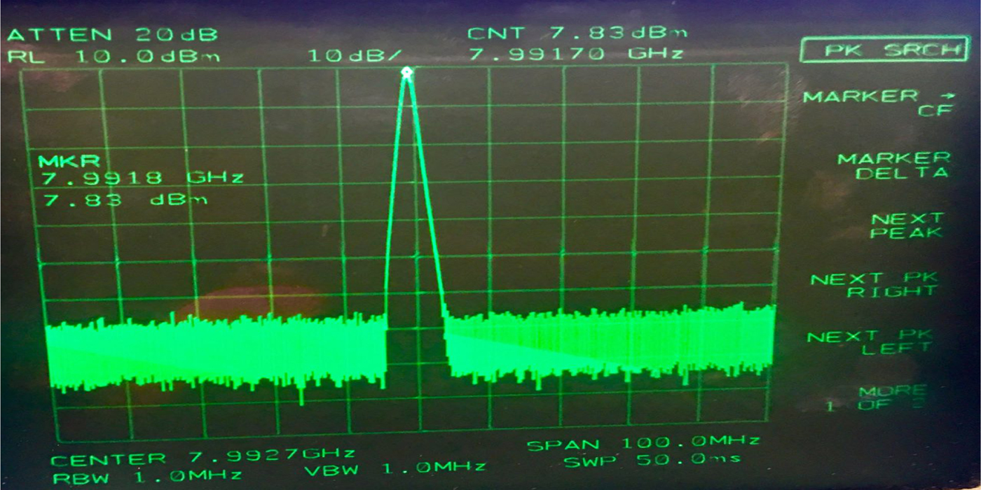
Fig. 18. Measured output power of proposed active DRO.
Since the phase noise of DRO is lower than the spectrum phase noise level, phase noise measurement was performed by the beating method, connecting two identical oscillators through a mixer. Figure 19(a) illustrates the block diagram of passive DRO measurement set up, Fig. 19(b) illustrates the block diagram of active DRO measurement set up and Fig. 19(c) depicts the active DRO experimental setup. It should be noted that there is a slight difference in oscillation frequency. Two oscillators are mixed using the double balanced mixer. This produces a down-converted signal with a frequency equal to 6.8 MHz. The phase noise of mixer output will be analyzed to investigate the effect of active feedback loop. It should be noted that the quoted value is 3 dB lower than the figure displayed on the plot. Therefore, it is necessary to subtract 3 dB from the measured value.

Fig. 19. Phase noise measurement (a) block diagram of passive DRO setup, (b) block diagram of active DRO setup, (c) active DRO experimental setup.
Figure 20 illustrates the phase noise of passive and proposed DRO. According to the result, it is equal to −145.19 dBc/Hz which leads to 12 dB improvement compared to passive DRO.

Fig. 20. Phase noise measurement results of passive and proposed DRO.
Table 1 compares the performance of the proposed method with other types of DROs with different topology and active devices. The figure of merit (FOM) is a factor that compares the oscillators in terms of resonance frequency, offset frequency, power consumption, and phase noise as described in equation (20) [Reference Tiebout23]. Results showed that the proposed active DRO has a better performance among different types of DROs.
 $$FOM = P.N-20\log \left( {\displaystyle{{\,f_0} \over {\Delta f}}} \right) + P_{DC}\lpar {dBm} \rpar .$$
Table 1. Performance comparison of different DROs

a The passive resonator oscillator.
b The proposed oscillator.
Conclusions
The main objectives of this paper are the development of extra low noise oscillators. A new structure for a low phase noise active DRO is presented which operates at 7.99 GHz. In order to achieve minimum phase noise, the structure of DR in the feedback loop is changed for the higher loaded quality factor. The key feature is to use a single active device in the proposed DRO. It overcomes the problem of the conventional active resonator oscillators such as complexity in structure, oscillation in spurious frequency, and low DC-to-RF efficiency. In addition, the performance showed that further phase noise reduction is possible. The best result was −145.19 dBc/Hz at 100 kHz offset frequency, 12 dB phase noise improvement in comparison to passive DRO. Subsequently, outcomes verify that by increasing the quality factor from 3651 to 6758, lower phase noise will be achieved.
Author ORCIDs
Shahrooz Asadi, 0000-0002-1816-3962.
Acknowledgement
I would also like to acknowledge Dr. Simon Bale, who helped build the Dielectric Resonator. Thanks must also go to the Technical Support Staff of University of York, and in particular to Mark Hough for fabricating the designed PCBs.
 Zahra Soltani received the B.Sc. and the M.Sc. degrees from Shahid Beheshti University, Tehran, Iran, both in electrical engineering, in 2011 and 2013, respectively. She is currently working toward the Ph.D. degree in the Department of electronic engineering Shahid Beheshti University, Tehran, IRAN. Since 2012, she has been involved in communication standard committee at National Iranian Gas Company (NIGC), Tehran, Iran. Her current research interests include high-Q microwave resonators, ultra-low-phase-noise oscillators and nonlinear simulation of microwave circuits.
 Shahrooz Asadi received the B.Sc. degree in Electrical Engineering and the M.Sc. degree in Electronics both from Amirkabir University of Technology (Tehran Polytechnic), in 2003 and 2007, respectively and the Ph.D. degree in Electronics in the School of Information Technology and Engineering (SITE), University of Ottawa, Ottawa, ON, Canada. He joined Shahid Beheshti University in 2011 where he is an assistant professor. His research interests include linear and nonlinear time-domain modeling of millimeter-wave transistors, RF design of active and passive devices, design and optimization of solid state devices and multiconductor transmission lines and printed circuit board.
 Esfandiar Mehrshahi received the B.Sc. degree from the Iran University of Science and Technology, Tehran, Iran, in 1987, and the M.Sc. and Ph.D. degrees from the Sharif University of Technology, Tehran, Iran, in 1991 and 1998, respectively, all in Electrical Engineering. Since 1990, he has been involved in several research and engineering projects at the Iran Telecommunications Research Center (ITRC). He is currently an Associated Professor at Shahid Beheshti University (SBU), Tehran, Iran. His main areas of interest are the nonlinear simulation of microwave circuits, low phase noise oscillators, and computational electromagnetics.


