I. INTRODUCTION
Nowadays the research community is very attentive to the energy consumption of radio systems and thus green radio is gaining momentum. However, the main challenge is to achieve a green radio without decreasing the gain achieved by fast radio which aims to increase data transmission rates [Reference Fettweis1].
Multi-antenna systems promise several key advantages such as higher data rates using spatial multiplexing and increased range using diversity coding and beamforming [Reference Winters2]. Nevertheless, the analog complexity issue concerning a multi-antenna receiver has been rarely addressed [Reference Kaiser, Bourdoux, Boche, Rodriguez Fonollosa, Bach Andersen and Utschick3].
In fact, the performance gain achieved by the antenna diversity implies an increase of the digital complexity (algorithms implementation), but also an increase of the complexity and the consumption of the analog front-end [Reference Tsurumi and Suzuki4]. Consequently, there will be considerable increase in power consumption and chip area.
Low power multi-antenna front-ends have already been proposed in [Reference Rafati and Razavi5, Reference Paramesh, Bishop, Soumyanath and Allstot6]. However, these structures are dedicated to restrictive diversity schemes (maximum ratio combining or beamforming) that can be implemented in the analog part of the receiver.
Therefore this paper deals with the architecture of the analog front-end that can be used by every multi-antenna scheme. A novel architecture for multi-antenna antenna receiver is proposed, it reduces the complexity of the analog front-end. This architecture is based on code multiplexing.
A similar method has just been recently approached by Tzeng et al. [Reference Tzeng, Jahanian and Heydari7, Reference Tzeng, Jahanian, Pi and Heydari8]. These papers assess the use of non-orthogonal codes [Reference Tzeng, Jahanian and Heydari7] and propose an interesting solution to design the analog coding [Reference Tzeng, Jahanian, Pi and Heydari8]. However, theoretical aspects, performance, and power consumption of the structure have not been assessed by other authors than us. Parts of this study have already been published in conferences [Reference Gautier, Burciu and Villemaud9–Reference Gautier and Villemaud11]; this paper presents a synthesis overview of the code multiplexing architecture.
So, in order to ensure the functionality of such a receiver, a global multi-antenna system has been developed by using an Agilent Technologies connected solution as presented in [Reference Morlat, Gallon and Villemaud12]. It includes radiofrequency (RF) impairments, realistic channels, and an antenna diversity algorithm.
This paper consists of five parts. Following this introduction, Section II presents the new multi-antenna front-end and simulation results are given including RF impairments. In Section III, a global multi-antenna system is implemented in order to achieve realistic performance. Section IV gives the evaluation of the complexity and power consumption of the proposed architecture. Finally, conclusions are drawn and follow-ups are provided.
II. THE CODE MULTIPLEXING ARCHITECTURE
In this first section, the code multiplexing architecture is presented by giving the theoretical aspects and some simulation results including RF impairments sensitivity. Parts of this section have already been published in [Reference Gautier, Burciu and Villemaud9, Reference Gautier, Morlat and Villemaud10].
A) State of the art and system model
In order to have a performance improvement, a transceiver using multi-antenna [Reference Winters2] has to use several antennas for its transmitter and/or its receiver. The state of the art of the multi-antenna analog front-end uses one dedicated analog chain for each of the antennas. This stack-up structure is shown in Fig. 1 at the receiver side where N is the number of the antennas. Each of these chains transforms the RF signal r k(t) in baseband signals [Reference Proakis13], in-phase I k(t) and in-quadrature Q k(t), k = 1, …, N.

Fig. 1. Stack-up architecture of a multi-antenna receiver.
The receiver of Fig. 1 uses a homodyne architecture [Reference Tsurumi and Suzuki4]. Each chain is composed of a surface acoustic wave RF filter dedicated to the band selection, a low noise amplifier (LNA) and an IQ demodulator used to recover the in-phase and in-quadrature baseband signals. The I k(t) and Q k(t) signals are then digitized by two analog-to-digital converters (ADC).
If we consider a single input multiple output transmission, the digital transmitted message is made of complex symbols x[i] which depends on the digital modulation (Quadrature amplitude modulation (QAM), Orthogonal Frequency Division Multiplexing (OFDM), etc.). These symbols are transmitted at the symbol rate D s = 1/T s, where T s is the symbol duration. The digital baseband signal (analog signal carrying digital information), with a rectangular pulse shaping, can be modeled by

The transmitted RF signal is real and it can be defined by
with f 0 the RF modulating frequency.
In an ideal transmission through a non-dispersive channel, the received signal on the kth antenna is expressed by
with h k the channel complex gain and n kRF(t) the total RF noise at the input of the kth antenna.
Once well filtered and amplified, the RF signal is translated in the baseband domain by an IQ demodulator. The baseband received contribution is
with n kRF (t) = Re[n kBB (t)e j2π f 0t].
This RF stack-up architecture is an obvious choice: having N separate dedicated chains allow the demodulation of each branch with a significant quality (high signal to noise ratio – SNR at the ADC input). However, this choice induces a high complexity to the analog front-end. The following structure aims to reduce this complexity without decreasing the SNR quality of the received baseband signal.
In [Reference Gautier and Villemaud11], we report the use of a single common front-end for the processing of signals received by the N antennas. The idea is to achieve decorrelation between the different branches in order to share a single analog reception chain.
Decorrelation can be performed by using the direct sequence spread spectrum (DSSS) technique. This technique allows a multiplexing, which is neither time nor frequency but a code multiplexing. Code multiplexing appears to be the best solution to achieve branches decorrelation without increasing RF constraints and without designing new components.
The novel multi-antenna receiver based on code multiplexing is shown in Fig. 2. The theoretical aspects of this structure are described in the next part.

Fig. 2. Analog and digital front-end of the code multiplexing architecture.
B) RF code multiplexing model
In this section, the DSSS technique is implemented in a multi-antenna receiver. The coding technique has two separate processing steps: an analog multiplexing of the RF signals and a digital demultiplexing of the different baseband components.
1) Analog coding
The DSSS consists in allocating a spreading code to each branch, all the codes being orthogonal two by two. The received signal carrying information is multiplied by the dedicated code, this code is a pseudo-random sequence of K binary entities having a rate K times higher than the symbol rate. Thus, the resulting signal has variations that are K times faster than the information signal, increasing K times the bandwidth of the signal's spectrum.
In order to perform the code multiplexing of all the branches, each received signal is spread using a code {c k(t), k = 1,…, N}. The pseudo-random sequences are T s-periodic. By using a limited symbol duration code, repeated indefinitely, the system has an easier sequence generation as well as a better despreading synchronization. For a given branch k, a set of K binary (complex binary) chips {c k[n], n = 1,…, K − 1} is used. This non-periodic sequence is called “spreading code” and is defined by
where T c is the chip duration and K = T s /T c is the code length.
The periodic code c kper (t) is the periodic pseudo-random sequence

The use of codes having a length of K allows the multiplexing of N signals only if N ≤ K.
Each received signal r k(t) is multiplied with its code c kper (t). Let d k(t) be the spread component of the kth antenna contribution. It is expressed by
By replacing s(t) by (2), we obtain

Once the coding operation is ended for each antenna, the new signals' intercorrelations depend only on the codes intercorrelations.
Hence, signals can be clearly overlapped in time and frequency, as they are separable by their spreading sequence. The adding operation between the spread contributions can be done

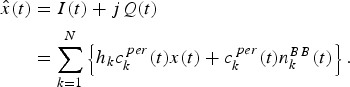
After the code multiplexing step, the signal d(t) is transposed from the RF to the baseband frequency by an IQ demodulator. Let I(t) be the in-phase component and Q(t) the in-quadrature component. LP[•] refers to an ideal low-pass filter having a bandwidth of B d/2 (where B d is the bandwidth of d(t)). I(t) and Q(t) are expressed by
After demodulation, the baseband signal is defined by its complex envelope
2) Digital decoding
So far, the different steps will be implemented in the analog part of the receiver. The decoding step will be performed digitally.
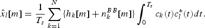
The pseudo-random sequence used for coding the symbols during the spreading step has to be known by the decoder in order to enable the reconstruction of symbols by successive correlations (despreading and integration on the symbol time) between the spread signal and the same coding sequence. Hence, after decoding, the lth antenna's contribution is expressed by
The intercorrelation properties influence the performance (detection and synchronization) of a system using the spread spectrum technique and which operates by correlation between signals and codes. The intercorrelation functions of the codes γk, l(τ) are defined by
If the codes are orthogonal, we have γk, l (0) = δ [k − l]. As a final result, we obtain
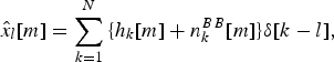
The digital baseband symbols {x l [m], l = 1, … N, m ∈ Z} received on each antenna are recovered.
According to (4) and (19), the theoretical performance of the code multiplexing architecture is similar to those of the stack-up architecture in a non-dispersive channel environment.
The proposed architecture works for any multi-antenna schemes: for every antenna array and every digital algorithm. Meanwhile, in order to achieve optimal efficiency, the number of antenna must be even and equal to the length of the code (i.e. N = K). The synchronization between coding and decoding is not such an important issue as for example during an Universal Mobile Telecommunications System (UMTS) transmission [Reference Schulze and Lueders14]. Indeed, the propagation delay of the spread signal through the circuit path is well-predicted through accurate circuit analysis and simulation. Therefore, attaining synchronization between the spreading and despreading codes is a trivial matter. For this reason, time delay between the spreading and despreading codes was neglected in this study.
C) Simulations results
The functionality of such a receiver is validated in this part by using several bit error rate (BER) simulations including RF impairments such as IQ imbalance and non-linearity. Two complete IEEE 802.11 g [15] transmission systems have been modeled using the advanced design system (ADS) software [16]: one using the stack-up front-end and the other using the code multiplexing front-end.
1) Systems description
The implemented systems are described in Figs 1 and 2. Each antenna receives an IEEE 802.11 g type signal. The channel bandwidth is 20 MHz, the RF frequency is 2412 MHz, and the data rate is 36 Mbit/s. For the code multiplexing architecture, the signals r k(t) are multiplied by the periodical spreading codes c kper (t). The sum of N encoded signals is then performed in order to generate the RF multiplex signal d(t). This signal is then transformed by an IQ demodulator. After the sampling step, we apply matched filters consisting of a digital filter (impulse response c k* [n]) followed by a subsampling operation.
We choose the Walsh–Hadamard codes [Reference Schulze and Lueders14] similar to those used by the UMTS standard. The signal r 1(t) from the first antenna is not spread because its associated code c 1(t) is only composed of “1.” Thus, the performance is given only for the second antenna which is coded by a non-unitary code c 2(t). We consider a perfect code synchronization.
2) BER performance
Simulated performance of the code multiplexing architecture is compared with the performance of a stack-up homodyne structure. The channel is an additive white Gaussian noise (AWGN), and N 0 being its power spectral density. The BER evolutions as a function of E b/N 0 are shown in Fig. 3 (E b is the energy per bit). This figure shows the influence of the number of multiplexed antennas on the BER evolution. N = 2, 4, and 8 antennas receivers are tested. We consider only the transmission quality of the second antenna, but similar results are obtained for each antenna.

Fig. 3. BER versus E b/N 0 for different numbers of antennas.
Simulation results show that, in an ideal no imperfection case (no multipath channel, no RF impairments), the structure using code multiplexing decreases the performance by less than 1 dB at a BER = 10−2 for an N = 2 antennas receiver. The E b/N 0 degradation increases with the number of antennas. It reaches 2.3 dB for an N = 8 antennas system.
This degradation is due to digital aliasing during the subsampling step after filtering. Indeed, due to the complexity of the ADS simulation software, the codes used in simulation are not perfectly orthogonal. Future work will address the reduction of this aliasing effect.
3) IQ imbalance study
This RF impairment characterizes the loss of orthogonality between the I and Q branches, due to a gain mismatch g and a phase mismatch φ between the two local oscillators [Reference Traverso, Ariaudo, Fijalkow, Gautier and Lereau17]. The phase mismatch is caused by a non-ideal layout which means that the lines between mixers are not strictly equal. The gain mismatch is due to a difference of the conversion gain between the I and Q mixers.
In [Reference Gautier, Morlat and Villemaud10], the IQ imbalance sensitivity of the code multiplexing receiver is assessed and we show that the resulting IQ imbalance influence is the same for each baseband contribution and is the same as for a single IQ demodulator [Reference Traverso, Ariaudo, Fijalkow, Gautier and Lereau17]. Figure 4 shows the normalized BER evolution depending on the gain and the phase imbalance. The power level conditions lead to a 10−3 level of BER for ideal IQ mismatch conditions. Simulated performance of the code multiplexing architecture is compared with the performance of a stack-up homodyne structure.

Fig. 4. Relative BER versus gain imbalance and versus phase imbalance.
According to theory, simulation results show that the new code multiplexing architecture has nearly the same sensitivity as the stack-up architecture.
4) PAPR study
The peak to average power ratio (PAPR) is a metric that characterizes the temporal variations of a signal. It is generally used to determine the dynamic range of the ADC.
In [Reference Gautier, Burciu and Villemaud18], the PAPR of the code multiplexing receiver is assessed and we show that the PAPR of the signal d(t) does not increase significantly with the multiplexing. In fact, for a small number of antennas (two or four), it has no influence on the number of bits of the ADC.
Figure 5 shows the complementary cumulative distribution function (CCDF) of the PAPR. In the study case introduced previously, we use 802.11 g signals that are based on OFDM modulation, the number of subcarriers is set to 128. The simulation results are compared to the OFDM theoretical CCDF [Reference Van Nee and Prasad19]. The results show that the PAPR increases slightly with the multiplexing, about 0.5 dB for a two antennas system and 1 dB for four antennas.

Fig. 5. CCDF as a function of PAPR.
III. EXPERIMENTAL VALIDATION
The functionality of such a receiver is validated in this section by several BER measurements. A global multi-antenna system has been realized for both structures. It uses an Agilent Technologies connected solution [Reference Morlat, Gallon and Villemaud12] in order to obtain realistic measurements. It uses the sample matrix inversion (SMI) algorithm in order to perform antenna diversity [Reference Gupta20].
Due to material constraints, the performance evaluation is performed only for a two antennas system. However, based on the results comparison between simulations and measurements with two antennas, a trend could be deduced for higher numbers of antennas, as done in [Reference Morlat, Gallon and Villemaud12].
A) Multi-antenna radio platform
1) Radio platform
For the experimental validation [Reference Morlat, Gallon and Villemaud12], the radio platform described in Fig. 6 is used. This platform is made of high technology equipments developed by Agilent Technologies [16]: one arbitrary waveform generator (ESG 4438C) and a vector spectrum analyzer (VSA89641) having two RF inputs. With this connected solution, a software/hardware interaction allows us to test and conceive very complex and realistic systems. We can therefore estimate the impact of the different noise sources of the RF front-end but also the impact of the propagation environment. Using the two RF inputs of the VSA allows us to analyze and evaluate the performance of a two antennas system.

Fig. 6. The platform structure for a 1 × 2 transmission.
2) Multi-antenna processing
The antenna diversity digital processing implemented here is the classical SMI [Reference Gupta20]. It uses the training sequence of the 802.11 g standard [15] in order to compute the optimal combination of different signals using an adaptive algorithm based on a minimum mean square error criterion. A simple adaptive algorithm is the least mean square which has a low complexity of O(N). But this algorithm has a very slow convergence. Taking into account that the training sequence time of an 802.11 g burst is short, it is preferable to use SMI which offers a faster convergence, even if SMI has an important O(N 3) complexity.
This algorithm is implemented by using a co-simulation structure using the ADS and the Matlab software.
B) Experimental results
First, the measurements are compared with the performance obtained by simulation in Fig. 3. The measures are given for both the code multiplexing architecture and the stack-up structure. BER measurements are realized for an AWGN channel and for different SNR levels at the antennas inputs, the SMI processing is not used in these first results. The BER evolutions of the second antenna are shown in Fig. 7.

Fig. 7. Simulated and measured BER versus E b/N 0 for a two antennas receiver.
Compared to the simulated results, the measured results are somewhat degraded. The difference is due to the channel used for the measurement which may not exactly be an AWGN one. The E b/N 0 gap between the stack-up and code multiplexing structures is almost the same during the measurements as that obtained during the simulations. It turns around 0.8 dB at a BER = 10−2.
In a second time, the performance of the SMI processing is evaluated in an AWGN and fading channel environment. The measured fading non-line-of-sight channel has been characterized in [Reference Morlat, Gallon and Villemaud12]. It is a two paths channel with a delay spread around 75 ns and an attenuation of 10 dB, the receiver velocity is around 12 km/h.
Figures 8 and 9 give the measurements performed with and without SMI processing for the two structures.

Fig. 8. Measured BER versus E b/N 0 with or without SMI in an AWGN channel.

Fig. 9. Measured BER versus E b/N 0 with or without SMI in a fading channel.
In an AWGN channel (Fig. 8), the BER evolutions show that a 3 dB gain is achieved for the two structures when using the SMI algorithm. This 3 dB processing gain corresponds to the theoretical result that a two antennas system should reach [Reference Sarkar, Wicks, Salazar-Palma and Bonneau21]. The structure using code multiplexing decreases the performance by less than 0.5 dB at a BER = 10−2 with and without SMI.
In a fading channel (Fig. 9), the diversity is growing and a 5 dB gain at BER = 10−2 is reached using the SMI algorithm. The gap between the two structures is almost the same as for the AWGN case.
IV. COMPLEXITY STUDY
We will now assess the complexity gain of the proposed structure (Fig. 2) compared to the stack-up architecture shown in Fig. 1 [Reference Gautier and Villemaud11]. First, a comparison study, in terms of number of components, has been done. Once this step is finished, another comparison study involving the power consumption of the analog front-end is done.
A) Complexity evaluation
Figure 2 shows a complete structure of the analog code multiplexing receiver. Each RF input branch is made of an antenna, an RF filter, and an LNA. The LNA output signals are multiplied with the codes before being added. The multiplication could be realized by a mixer that multiplies a low-frequency signal (the code) and an RF signal. The multiplex RF signal is then transposed to baseband frequency by an IQ demodulator.
Table 1 reveals the number of components required for each structure and some constraints associated with these components. We consider that N is the number of antennas, B c is the channel bandwidth, f 0 is the RF standard center frequency, and BW stands for bandwidth.
Table 1. Number of components for the front-end using a stack-up and a code multiplexing architecture.

Regardless of technological constraints, the major difference between the two structures is the number of mixers and ADC. The proposed structure reduces by an N factor the number of ADC compared to the stack-up structure. This complexity gain should induce an important reduction of the chip area. In order to take into account the technological constraints, we propose a power consumption evaluation in the next section.
The digital complexity of the matched filters (N filters using N coefficients) is neglected in this analysis. The reason is that the additional complexity of this processing is not important compared to the initial complexity of algorithms needed to perform the multi-antenna processing.
The code synthesis is an important part of the structure which is not presented in this paper. A digital generation of the code has been proposed as a solution, its complexity is therefore neglected in this analysis.
B) Power consumption
To evaluate the power consumption, we consider a standard using a multi-antenna receiver: IEEE 802.11 g having a channel bandwidth of B c = 20 MHz.
Among the components of Table 1, the antennas, the filters, and the adder are passive components whereas the LNA and the mixers have exactly the same characteristics for both stack-up and code multiplexing architecture. Therefore, this study takes into account the power consumption P W for the LNA, the mixers, and the ADC
where N LNA, N Mixer, and N ADC are the number of the LNA, of the mixers, and of the ADC given in Table 1. P LNA, P Mixer, and P ADC are the power consumption of one of the LNA, of the mixers, and of the ADC, respectively.
As a mixer, we propose to use the MAX 2682 component from MAXIM for the two structures. This component has a power consumption of P Mixer = 45 mW.
As an LNA, we propose to use the mixer introduced in [Reference Liao and Chuang22] for the two structures. This component has a power consumption of P LNA = 15 mW.
To determine P ADC, we use the figure of merit given by [23]
with ENOB being the effective number of bits (we choose ENOB = 10 bits [Reference Tsurumi and Suzuki4]) and f s the sample rate (f s = 4B s for IEEE 802.11 g standard with B s the sampling bandwidth). The value given in 2007 by System drivers [23] concerning the FoM ADC is 1200 GHz/W.
B s is equal to B c for the stack-up architecture and to NB C for the code multiplexing architecture.
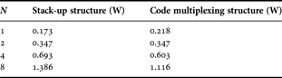
Table 2 gives the power consumption P W for different number of antennas.
Table 2. Power consumption for IEEE 802.11 g reception.

Results show that the proposed structure reduces significantly the power consumption of a multi-antenna front-end. In fact, if the number of antennas is higher than two, the consumption model shows that the code multiplexing structure clearly outperforms the stack-up structure. A consumption reduction of 20% is reached for N = 8 antennas.
V. CONCLUSION
In this paper, we present a novel architecture for a multi-antenna receiver. The proposed structure uses orthogonal codes to multiplex the different branches through a single IQ demodulator. The main objective was to reduce the complexity of the analog front-end.
First, we assess the feasibility of such a structure. The implementations of analog coding and digital decoding have been validated by realistic BER simulations that include the RF impairments. Then the code multiplexing architecture has been tested in a global multi-antenna system with an SMI processing and realistic channels. In all cases, we show that the code multiplexing structure does not decrease significantly the performance of the system when compared to the stack-up architecture.
The last points revealed in this study are the gains in terms of chip area and power consumption. The system reduces the number of ADC by using only 2 ADC instead of the 2N used by the stack-up receiver. Meanwhile, specifications of the ADC in terms of bandwidth are much more stringent.
By taking into account the performance and the power consumption, the proposed structure should be very interesting for a system with four antennas.
The follow-ups of this work are to accurately define the specifications of the analog components in order to realize an integration of the structure. An extension to multi-channel receiver has to be studied as well as its resulting complexity-performance trade-off.
ACKNOWLEDGEMENT
The authors would like to thank Orange Labs which support this study.
 Matthieu Gautier was born in Poissy, France, on June 3, 1978. He has received M.Sc. degree in signal and image processing from the University of Cergy-Pontoise, France, and an electrical engineering degree from the ENSEA both in 2001. In March 2006 he received a Ph.D. degree from the INPG Grenoble, France. From September 2006 to September 2009, he was a post-doctoral researcher at Orange labs and at CITI laboratory. He is currently a research engineer at the CEA-LETI laboratory. His research interest is signal processing for wireless communication: wavelet packet modulation, multi-antenna multi-standard system, radio architecture, and RF impairments.
 Guillaume Villemaud was born in Limoges, France, in 1973. He received M.S. degree in electrical engineering from the University of Limoges, France, in 1999. From1999 to 2002 he worked at IRCOM, Limoges, France, on compact integrated antennas and received his Ph.D. degree in electronics in 2002. He developed multi-band hybrid arrays for CREAPE from 2002 to 2003 and then joined the CITI Laboratory, Lyon, France, in 2003. He is currently an associate professor at INSA Lyon, France. His research interests are antenna design and integration, antenna diversity and multiple antenna processing (SIMO, MIMO), and system level simulation and measurements.
 Ioan Burciu was born in Craiova, Romania, in 1982. He received the diploma degree in electrical engineering and the M.Sc. degree in microelectronics engineering from INSA, Lyon, France, both in 2006 and is currently working toward the Ph.D. degree in telecommunications engineering at Orange Labs R&D Center, Meylan, France as well as at CITI Laboratory, Lyon, France. His research interests are radiofrequency design and implantation, system level simulation and measurements as well as multiple antennas processing (SIMO, MIMO).