


I. INTRODUCTION
Metamaterial transmission lines (a type of artificial transmission lines) have been widely applied in the microwave field due to their unique and controllable propagation properties [Reference Caloz and Itoh1, Reference Marqués, Martín and Sorolla2]. One of their applications is multi-band devices, where the composite right-/left-handed transmission line (CRLH TL) concept [Reference Lin, De Vincentis, Caloz and Itoh3, Reference Eleftheriades, Iyer and Kremer4] has been extensively used for design of dual-band components. This dual-band functionality has been achieved thanks to the presence of a left-handed and a right-handed band, and to the controllability of the dispersion characteristics.
Metamaterial transmission lines with more than two propagation bands are also possible. This feature enhances CRLH TL functionality and allows the realization of devices with a higher number of operative bands. However, the requirement of a higher number of bands also leads to an artificial line with a higher number of reactive elements. In [Reference Rennings, Otto, Mosig, Caloz and Wolff5, Reference Eleftheriades6], an artificial line with four different operative bands was proposed, and the resulting artificial line was called extended-composite right-/left-handed transmission line (E-CRLH TL). Although several dual-band or quad-band devices based on E-CRLH TL have been reported [Reference Rennings, Otto, Mosig, Caloz and Wolff5–Reference Ryan and Eleftheriades13], most components required the inclusion of lumped elements [Reference Studniberg and Eleftheriades7, Reference Papanastasiou, Georghiou and Eleftheriades9, Reference Studniberg and Eleftheriades10], or presented some disagreement between circuit and electromagnetic simulation [Reference Chen, Zhang, Wu and Seo8, Reference Ryan and Eleftheriades13] (this complicates device design and the goal to satisfy specific requirements).
In [Reference Durán-Sindreu, Sisó, Bonache and Martín11, Reference Durán-Sindreu, Sisó, Bonache and Martín12], a fully-planar E-CRLH TL was presented both in microstrip and CPW technology, where an accurate circuit model that explains the behavior of the structure was shown. Nonetheless, due to the complexity of the design and the technologies considered, the reported E-CRLH TL based components suffered from high losses. This may jeopardize the application requirements, especially when increasing the frequency range. These problems can be solved by considering substrate-integrated waveguides (SIWs), i.e. planar structures that can mimic a rectangular waveguide using low-cost standard PCB fabrication process. SIWs are implemented by arranging two rows of metallized via holes throughout two metal plates embedded in a dielectric substrate. By this means, higher-quality factor (and therefore lower-losses) and higher-power capability, as compared with microstrip or CPW transmission lines, can be obtained. Moreover, SIW transmission lines can potentially operate up to the millimeter-wave region [Reference Deslandes and Wu14–Reference Deslandes and Wu16]. This technology has been proven to support both forward and backward waves by loading the SIW line with interdigital series capacitors [Reference Zhao, Cui, Lin and Ma17, Reference Dong and Itoh18]. The equivalent CRLH TL behavior is obtained due to the combination of this capacitance with the inherent series inductance and shunt inductance/capacitance of the SIW structure. In [Reference Durán-Sindreu, Bonache, Martín and Itoh19], the implementation of an E-CRLH TL based on SIW technology was proposed for the first time, where the presence of four transmission bands (two left-handed and two right-handed bands) was demonstrated by reporting a quad-band power divider. As compared to any other reported E-CRLH TL (to the authors' knowledge), the presented SIW-based structure was also the first fully-planar E-CRLH TL only involving the etching of a single metal layer, and hence reducing fabrication complexity. In this extended paper of [Reference Durán-Sindreu, Bonache, Martín and Itoh19], the application of these SIW-based E-CRLH TLs to the design of dual-band band-pass filters (including third- and fifth-order filters with standard Chebyshev responses) is also reported. Hence, the potential of these SIW-based structures for implementation of dual-band and quad-band devices will be demonstrated.
The paper is organized as follows: In Section II, the topology and circuit model of the SIW-based E-CRLH TLs is presented and discussed. In Section III, the application of this structure to the design and implementation of quad-band devices is demonstrated through a quad-band Y-junction power divider. The design of dual-band band-pass filters is reported in Section IV. Finally, the main conclusions of the paper are highlighted in Section V.
II. TOPOLOGY AND CIRCUIT MODEL OF THE SIW-BASED E-CRLH TLS
The equivalent circuit model (unit cell) of an E-CRLH TL [Reference Rennings, Otto, Mosig, Caloz and Wolff5, Reference Eleftheriades6] is depicted in Fig. 1. This circuit exhibits four different propagation bands (two left-handed and two right-handed bands), allowing the possibility to force four arbitrary phase and impedance conditions at four different frequencies. For the lossless symmetric T-model configuration of Fig. 1, the propagation constant, β, in the regions where wave propagation is allowed, and the Bloch impedance Z B(ω) are given by
 $$\cos \beta l=1+\displaystyle{{Z_s \lpar \omega \rpar } \over {Z_p \lpar \omega \rpar }}$$
 $$Z_B \left(\omega \right)=\sqrt {Z_s \left(\omega \right)\lsqb Z_s \left(\omega \right)+2Z_p \left(\omega \right)\rsqb }$$
where Z s(ω) and Z p(ω) are the series and shunt impedances of the T-circuit model of the E-CRLH TL, respectively, and l is the length of the structure. Thus, by setting the four conditions of phase and impedance through equations (1) and (2), the eight element values of the circuit of Fig. 1 are, in general, univocally determined (under some circumstances, it is possible that the resulting system of equations does not provide physically acceptable solutions for the reactive elements, i.e. real positive values). In addition, depending on the application requirements, a different set of equations will result. For this reason, the design-oriented equations for different types of applications will be discussed in each section.

Fig. 1. Unit cell of an E-CRLH TL.
The proposed topology to implement an E-CRLH TL in SIW technology is depicted in Fig. 2. Series and shunt interdigital slots are considered to model the capacitances [Reference Zhao, Cui, Lin and Ma17, Reference Dong and Itoh18, Reference Dong and Itoh20], with the exception of the capacitance C vp, which is implemented by the SIW host line. The required inductances are implemented and controlled by the interdigital fingers and/or the SIW host line. Moreover, an additional slot in the series branch can be considered to increase the L hs inductance value. In order to accurately explain the full behavior of this structure, additional shunt elements are required to model the distributed shunt inductance and capacitance of the SIW cavity, as shown in Fig. 3. Nonetheless, as will be seen, the existence of these parasitics (L 1, C 1, L 2 and C 2) does not avoid the presence and controllability of the four bands.

Fig. 2. Topology of the SIW based E-CRLH TL. The top metal is indicated in gray, whereas the vias are indicated in black. Dimensions are: a = 5.66 mm, b = 3.34 mm, W = 28.34 mm, and L = 15.1 mm. All the interdigital capacitors have a separation between fingers (gap) of 0.12 mm. The fingers width (w i) and length (l i) of the interdigital capacitors are: for the series capacitors (from left to right): w 1 = 0.24 mm, l 1 = 1.52 mm and w 2 = 0.285 mm, l 2 = 1.02 mm. For the shunt branch: w 3 = 0.25 mm and l 3 = 5.72 mm. The vertical slot has a width of 0.41 mm and length of 11.04 mm. The vias have a radius of 0.4 mm and a center-to-center distance between vias of 1.4 mm.

Fig. 3. Accurate equivalent circuit model of the SIW based E-CRLH TL topology of Fig. 2.
III. QUAD-BAND APPLICATIONS (Y-JUNCTION POWER DIVIDER)
The unit cell of Fig. 2 can be applied to implement quad-band devices. To this end, equations (1) and (2) can be considered to force the required impedance and phase conditions. Thus, the eight circuit elements of the equivalent circuit of Fig. 1 are analytically obtained; then, an initial tentative layout that satisfies these conditions can be inferred by curve fitting the series and shunt reactances of the equivalent T-circuit model of Fig. 3 and the full-wave electromagnetic simulation. This step is required to obtain the parasitic values of the SIW cavity L 1, C 1, L 2 and C 2. These parasitics are determined and controlled by means of the size of the cavity, each pair of inductance and capacitance forming an LC tank with a resonance frequency
 $$\omega _{0_1 }=\displaystyle{1 \over {\sqrt {L_1 C_1 } }}$$
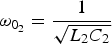 $$\omega _{0_2 }=\displaystyle{1 \over {\sqrt {L_2 C_2 } }}$$
Since at these resonance frequencies the impedance of the parasitic tanks goes to infinity, a possible solution to reduce the impact of parasitics on the frequency response around the regions of operation is to set these resonances at the average point between the four bands. Nonetheless, this latter condition is not strictly required to satisfy the requirements, thus having some additional flexibility to choose the cavity size. Once these parasitic values are set and known, the final element values that satisfy the requirements can be obtained through equations (1) and (2) considering the equivalent circuit of Fig. 3 and the inferred parasitic elements. In order to do this, the equivalent symmetric T-circuit model of Fig. 3 can be obtained through manipulation of the [ABCD] matrix. Finally, the definite layout is inferred by curve fitting the circuit and electromagnetic reactances.
This procedure has been applied to the design of a quad-band impedance inverter (βl = ±90°) operative at the frequencies f 1 = 3.75 GHz, f 2 = 4.46 GHz, f 3 = 5.15 GHz, and f 4 = 5.9 GHz. The impedance condition has been set to Z B = 35.35 Ω to subsequently apply this inverter to the implementation of a quad-band Y-junction power divider. The eight equations that result from (1) and (2) with this impedance condition and by setting the phase to βl = −90° at f 1 (first left-handed band) and f 3 (second left-handed band) and βl = +90° at f 2 (first right-handed band) and f 4 (second right-handed band) are:
 $$\chi _s \lpar f_n \rpar =\lpar \! - 1\rpar ^n Z_B$$
 $$\chi _p \lpar f_n \rpar =\lpar \! - 1\rpar ^{n+1} Z_B$$
where n = 1, 2, 3, and 4 is the frequency index, and χs(ω) and χp(ω) are the reactances of the series and shunt branch of the T-circuit model (i.e. Z s(ω) = jχs(ω) and Z p(ω) = jχp(ω)).
The ideal values that satisfy these requirements (i.e., the ones that correspond to the model of Fig. 1 without parasitics) are: L hs = 7.707 nH, C hs = 0.151 pF, L hp = 0.121 nH, C hp = 8.99 pF, L vs = 5.617 nH, C vs = 0.193 pF, L vp = 0.3777 nH, and C vp = 3.084 pF. With these values, a first tentative layout is obtained and the parasitics are inferred, where the conditions L 1 = L 2 and C 1 = C 2 have been set to simplify the design process (given its similar values for this specific layout). The values of these elements are L 1 = L 2 = 5.5 nH and C 1 = C 2 = 0.2 pF, satisfying that its resonance frequency is at the mid-point between the four bands. Considering these parasitics, the final element values corresponding to the circuit of Fig. 3 are re-calculated, being: L hs = 6.353 nH, C hs = 0.184 pF, L hp = 0.117 nH, C hp = 9.27 pF, L vs = 5.23 nH, C vs = 0.207 pF, L vp = 0.358 nH, and C vp = 3.26 pF. The resulting layout satisfying these requirements, obtained by curve fitting the responses, is shown in Fig. 2, where the Rogers 5880 substrate with ɛ r = 2.2, thickness h = 1.27 mm, and loss tangent tanδ = 0.001 has been considered. The comparison between circuit and electromagnetic simulation (considering the lossless case and 35.35 Ω ports) of the series and shunt reactances of the equivalent T-circuit model is depicted in Fig. 4. The magnitude and phase responses are also compared in Fig. 5 (the Agilent ADS circuit and electromagnetic simulators have been used). As can be seen, the conditions of phase and impedance are simultaneously satisfied at the required four frequency bands (3.75, 4.46, 5.15, and 5.9 GHz), and very good agreement between the circuit model and the electromagnetic simulation is obtained, thus validating both the model and the methodology.

Fig. 4. Series χs and parallel χp reactances of the equivalent T-circuit model of the quad-band impedance inverter SIW based E-CRLH TL layout of Fig. 2. The corresponding circuit values of the accurate circuit model of Fig. 3 are: L 1 = L 2 = 5.5 nH, C 1 = C 2 = 0.2 pF, L hs = 6.85 nH, C hs = 0.16 pF, L hp = 0.117 nH, C hp = 9.27 pF, L vs = 5.23 nH, C vs = 0.207 pF, L vp = 0.358 nH, and C vp = 3.26 pF.

Fig. 5. Simulated magnitude (a) and phase (b) response of the quad-band impedance inverter SIW based E-CRLH TL topology of Fig. 2, considering 35.35 Ω ports. The circuit values used in the circuit simulation are those shown in the caption of Fig. 4. The four frequency positions where the phase and impedance conditions are satisfied have been highlighted with circles.
In order to demonstrate the quad-band functionality of the proposed SIW based E-CRLH TL, a quad-band Y-junction power divider has been designed by adding two 50 Ω output ports and access lines to the quad-band impedance inverter of Fig. 2. This device has been fabricated by using standard photo/mask etching techniques. The photograph of the resulting device is shown in Fig. 6. The comparison between electromagnetic simulation (considering ohmic and dielectric losses) and measurement (obtained by means of the Agilent 8510C network analyzer) is shown in Fig. 7. It is also worth noting that even though the quad-band conditions are only satisfied at the designed frequencies, the power divider functionality is expanded between the first two bands and the last two bands, generating thus an equivalent dual-band band-pass behavior.

Fig. 6. Photograph of the fabricated SIW quad-band Y-junction power divider based on the quad-band impedance inverter of Fig. 2.

Fig. 7. Measured and simulated frequency response of the SIW quad-band power divider of Fig. 6. The frequencies of operation are f 1 = 3.75 GHz, f 2 = 4.46 GHz, f 3 = 5.15 GHz, and f 4 = 5.9 GHz.
Good agreement between different responses is obtained. Measured performance is good, with insertion losses at different bands lower than 4.5 dB (3 dB being the minimum insertion losses of an ideal two-output power divider) except for the third band, being below 7.5 dB due to its smaller bandwidth and proximity to transmission zero. Measured return losses are better than 16, 24, 34.5 and 46 dB for the first, second, third, and fourth band, respectively. The total size of the fabricated device (excluding access lines) is 15.1 × 28.34 mm, which corresponds to 0.19λ 0 × 0.35λ 0 for the first (lowest) frequency band and 0.3λ 0 × 0.56λ 0 for the fourth (highest) frequency band, λ 0 being the free-space wavelength.
IV. DUAL-BAND APPLICATIONS (BAND-PASS FILTERS)
The presented SIW-based E-CRLH TL can also be applied to the design of dual-band devices with higher requirements. This is the case of band-pass filters with standard Chebyshev responses, where the additional conditions of equal ripple and controlled bandwidth lead to a dual-band functionality description through the equivalent circuit of Fig. 1 [Reference Durán-Sindreu, Sisó, Bonache and Martín12, Reference Durán-Sindreu, Bonache and Martín21]. The values of the circuit elements can be inferred through control of the dispersion and impedance in a similar way as the one explained in Section III [Reference Eleftheriades6, Reference Eleftheriades22, Reference Eleftheriades23]. Nonetheless, in this case we will obtain these elements by means of successive low-pass transformations [Reference Durán-Sindreu, Sisó, Bonache and Martín12, Reference Guan, Ma, Cai, Kobayashi, Anada and Hagiwara24]. This allows simple closed-form equations, as well as the implementation of higher-order filters (periodicity not being a requirement). However, this approach only allows implementing narrow-band dual-band band-pass filters with equal fractional bandwidth (FBW) at both bands.
The methodology to implement dual-band band-pass filters by means of this latter approach is as follows: first, the element values of Fig. 1 are obtained through the equations reported in [Reference Guan, Ma, Cai, Kobayashi, Anada and Hagiwara24]. Then, a tentative layout is generated to infer the value of the SIW parasitics. Later, an optimization is applied to the schematic (circuit level) by forcing the parasitics to the values obtained in the previous step to satisfy the filter requirements. This can be realized by forcing the frequency positions of the matching points of the Chebyshev response at each filter pass band. Finally, the layout that satisfies the modified (optimum) circuit elements considering parasitics is obtained through curve fitting. It is worth noting that standard Chebyshev responses can be obtained to a very good approximation even in the presence of parasitics. In fact, these parasitics improve the lower and upper selectivity of the first and second band, respectively. This is due to the parasitic inductive and capacitive behavior below the first band and above the second band, respectively. This can be seen in Fig. 8, where an example of a third-order dual-band band-pass filter with central frequencies 4.1 and 5.6 GHz, FBW = 23% and ripple of 0.1 dB is considered for the two cases (with and without parasitics). From this figure, it can be observed that parasitics do not alter the response in the pass band regions, but they improve filter selectivity, making this approach very attractive for filter applications.

Fig. 8. Frequency response of a dual-band band-pass filter with and without parasitics. The specifications of the filter are: central frequencies 4.1 and 5.6 GHz, FBW = 23% and ripple = 0.1 dB.
This methodology has been applied to the design of a third-order dual-band band-pass filter with the same specifications as the example proposed for Fig. 8. The ideal element values that satisfy these specifications are (in reference of Fig. 1): L hs = 7.359 nH, C hs = 0.15 pF, L hp = 0.18 nH, C hp = 6.119 pF, L vs = 6.877 nH, C vs = 0.16 pF, L vp = 0.674 nH, and C vp = 1.637 pF. The modified circuit elements after inferring the parasitics and optimizing the response at the circuit level are (in reference of Fig. 3): L 1 = L 2 = 5.5 nH and C 1 = C 2 = 0.2 pF, L hs = 7.875 nH, C hs = 0.14 pF, L hp = 0.16 nH, C hp = 6.896 pF, L vs = 5.902 nH, C vs = 0.187 pF, L vp = 0.555 nH, and C vp = 1.986 pF. The layout and photograph of the fabricated structure, considering the Rogers 5880LZ substrate with ε r = 1.96, thickness h = 1.27 mm, and loss tangent tanδ = 0.002, is shown in Fig. 9, and the frequency response is depicted in Fig. 10. As can be seen, good agreement between measurement, electromagnetic, and circuit simulation (considering parasitics) is obtained, with measured return losses better than 10 dB and insertion losses below 1 and 1.5 dB for the first and second band, respectively. The first spurious appears at 8.2 GHz and a rejection level better than 10 dB is maintained up to 9 GHz, i.e. 1.9f 0, f 0 being the geometric mean between the two pass band central frequencies. The size of the device is 14.3 mm × 28.34 mm, which corresponds to 0.23λ 0 × 0.45λ 0 at f 0.
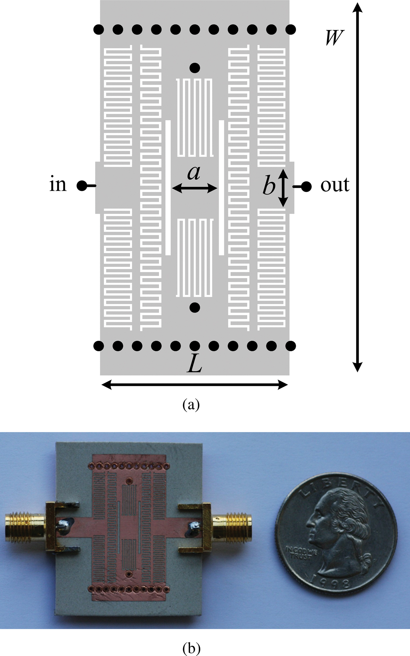
Fig. 9. Topology (a) and photograph (b) of the fabricated SIW based third-order dual-band band-pass filter. Dimensions are: a = 3.63 mm, b = 3.15 mm, W = 28.34 mm, and L = 14.3 mm. The fingers width (w i), length (l i), and separation between fingers (gap g i) of the interdigital capacitors are: for the series capacitors (from left to right): w 1 = 0.24 mm, l 1 = 1.96 mm, g 1 = 0.16 mm and w 2 = 0.285 mm, l 2 = 1.43 mm, g 2 = 0.18 mm. For the shunt branch: w 3 = 0.25 mm, l 3 = 5.76 mm, and g 3 = 0.16 mm. The vertical slot has a width of 0.41 mm and length of 10.19 mm. The vias have a radius of 0.4 mm and a horizontal and vertical center-to-center distance between vias of 1.45 mm and 2.9 mm, respectively.

Fig. 10. Measured and simulated frequency response of the third-order dual-band band-pass filter of Fig. 8.
Higher-order dual-band band-pass filters can also be implemented with this type of structure. To demonstrate this, a fifth-order (non-periodic) dual-band band-pass filter with the same specifications as the previous case is reported. The resulting layout is shown in Fig. 11(a). The interdigital capacitors of the central stage that act as series resonators have been split into two capacitors to maintain symmetry conditions with the vertical slots, as well as to keep a symmetric equivalent circuit. Thus, the central series branch stage can be modeled with the equivalent circuit shown in Fig. 12, where an automatic optimization procedure of the complete equivalent fifth-order filter can still be applied. The ideal element values that satisfy the Chebyshev specifications are (in reference of Fig. 1, from left to right): L hs1 = L hs3 = 8.181 nH, L hs2 = 14.089 nH, C hs1 = C hs3 = 0.135 pF, C hs2 = 0.078 pF, L hp1 = L hp3 = 0.2 nH, L hp2 = 0.345 nH, C hp1 = C hp3 = 5.504 pF, C hp2 = 3.196 pF, L vs2 = L vs4 = 5.754 nH, C vs1 = C vs2 = 0.192 pF, L vp1 = L vp2 = 0.564 nH, and C vp1 = C vp2 = 1.956 pF. The modified circuit elements after inferring the parasitics and optimizing the response at the circuit level are (in reference of Figs 3 and 12 for the external and central stages, respectively): L 1 = L 2 = 5.5 nH and C 1 = C 2 = 0.2 pF, L hs1 = L hs3 = 9.5 nH, L hs2 = 7.256 nH, C hs1 = C hs3 = 0.116 pF, C hs2 = 0.151 pF, L hp1 = L hp3 = 0.214 nH, L hp2 = 0.173 nH, C hp1 = C hp3 = 5.193 pF, C hp2 = 6.392 pF, L vs1 = L vs2 = 4.948 nH, C vs1 = C vs2 = 0.222 pF, L vp1 = L vp2 = 0.504 nH, and C vp1 = C vp2 = 2.195 pF, where the shown modified circuit values C hs2 and L hs2 considering parasitics correspond to those of each interdigital capacitor individually (see Fig. 12). In Figs 11(a), (b) and 13, the layout, photograph and frequency response of the fabricated device is shown, respectively. Measured return losses better than 10 dB in both bands and insertion losses better than 1.7 and 3 dB for the first and second band, respectively, are obtained. The first spurious appears at 7.8 GHz, maintaining a 10 dB rejection up to 9.1 GHz (as the case of the third-order filter). The size of the device is 27.3 mm × 28.34 mm, which corresponds to 0.44λ0 × 0.45λ0 at f 0.

Fig. 11. Topology (a) and photograph (b) of the fabricated SIW based fifth-order dual-band band-pass filter. The numeration at the top indicates the sub index for the dimensions of each interdigital capacitor. Dimensions are: a = 4.53 mm, b = 0.98 mm, c = 2.42 mm, W = 28.34 mm, and L = 27.3 mm. The fingers width (w i), length (l i), and separation between fingers (gap g i) of the interdigital capacitors are: For the series capacitors of the external stages (from left to right): w 1 = w 9 = 0.24 mm, l 1 = l 9 = 1.87 mm, g 1 = g 9 = 0.17 mm and w 2 = w 8 = 0.285 mm, l 2 = l 8 = 1.4 mm, g 2 = g 8 = 0.2 mm. For the series capacitors of the central stage (from left to right): w 4 = w 6= 0.285 mm, l 4 = l 6 = 1.46 mm, g 4 = g 6 = 0.18 mm and w 5 = 0.24 mm, l 5 = 1.68 mm, and g 5 = 0.18 mm. For the shunt branch: w 3 = w 7 = g 3 = g 7 = 0.24 mm, l 3 = l 7 = 6.04 mm. The vertical slot has a width of 0.41 mm and length of 11.15 mm. The vias have a radius of 0.4 mm and a horizontal and vertical center-to-center distance between vias of 2.05 mm and 2.8 mm, respectively.

Fig. 12. Accurate equivalent circuit model of the SIW-based E-CRLH TL central series branch stage of Fig. 11.

Fig. 13. Measured and simulated frequency response of the fifth-order dual-band band-pass filter of Fig. 11. The circuit simulation corresponds to the case considering parasitics.
V. CONCLUSIONS
The implementation and potential applications of a novel single-layer fully-planar E-CRLH TL based on SIW technology have been proposed. The quad-band functionality of the reported artificial lines has been proven by designing and fabricating a quad-band Y-junction power divider, where good agreement between simulation and measurement has been obtained. The dual-band functionality has been demonstrated by designing and fabricating an order-3 and an order-5 Chebyshev dual-band band-pass filter. As compared to previous E-CRLH TLs, the proposed approach involves etching only the upper metallic level of the PCB. Lumped elements are not needed, and the backside metal is kept unaltered. Moreover, as compared to other fully planar E-CRLH TLs [Reference Durán-Sindreu, Sisó, Bonache and Martín11, Reference Durán-Sindreu, Sisó, Bonache and Martín12, Reference Durán-Sindreu, Bonache and Martín21], the reported prototypes operate up to the C-band, exhibiting very reasonable performance. Therefore, SIW-based E-CRLH TLs are very promising in applications where multiband functionality compatible with low cost fabrication processes and backside isolation are fundamental aspects.
ACKNOWLEDGEMENT
This work was supported by MICIIN-Spain (contract TEC2010-17512 METATRANSFER), Generalitat de Catalunya (project 2009SGR-421) and by MICIIN-Spain (project CONSOLIDER EMET CSD2008-00066). Miguel Durán-Sindreu is also in debt to Universitat Autònoma de Barcelona for supporting his stay at the University of California, Los Angeles.
 Miguel Durán-Sindreu was born in Barcelona, Spain, in 1985. He received the Telecommunications Engineering diploma, Telecommunications Engineering degree, and Ph.D. degree from the Universitat Autònoma de Barcelona, Bellaterra, Spain, in 2007, 2008, and 2011, respectively. Throughout his professional career, he has worked at different research centers such as Technische Universität Darmstadt (Germany) in 2010 and University of California, Los Angeles (USA) in 2011. His research interests are microwave devices, metamaterials, and multiband components.
 Jordi Bonache was born in Cardona (Barcelona), Spain, in 1976. He received the Physics and Electronics Engineering degrees and Ph.D. degree in electronics engineering from the Universitat Autònoma de Barcelona, Bellaterra (Barcelona), Spain, in 1999, 2001, and 2007, respectively. In 2000, he joined the High Energy Physics Institute of Barcelona (IFAE), where he was involved in the design and implementation of the control and monitoring system of the MAGIC telescope. In 2001, he joined the Department d'Enginyeria Electrònica, Universitat Autònoma de Barcelona, where he is currently an Assistant Professor. His research interests include active and passive microwave devices and metamaterials.
 Ferran Martín received the B.S. degree in physics and Ph.D. degree from the Universitat Autònoma de Barcelona, Bellaterra, Spain, in 1988 and 1992, respectively. Since 2007, he has been Full Professor of Electronics with the Departament d'Enginyeria Electrònica, Universitat Autònoma de Barcelona (UAB). He is very active in the field of metamaterials and their application to the miniaturization and optimization of microwave circuits and antennas. He is the head of the Microwave and Millimeter Wave Engineering Group (GEMMA Group) at UAB, and director of CIMITEC, a research Center on Metamaterials supported by TECNIO (Generalitat de Catalunya). He has authored and co-authored over 350 technical conference, letter, and journal papers, and he is the coauthor of the monograph on metamaterials, entitled Metamaterials with Negative Parameters: Theory, Design and Microwave Applications (Wiley, 2008). He has filed several patents on metamaterials and has headed several development contracts.
Dr Martín received the 2006 Duran Farell Prize for Technological Research, he holds the Parc de Recerca UAB—Santander Technology Transfer Chair, and he was the recipient of an ICREA ACADEMIA Award. He has organized several international events on metamaterials, including workshops at the IEEE Microwave Theory and Techniques Society (IEEE MTT-S) International Microwave Symposium (years 2005 and 2007) and European Microwave Conference (2009). He was the guest editor for three Special Issues on metamaterials in three international journals.
 Tatsuo Itoh received the Ph.D. Degree in Electrical Engineering from the University of Illinois, Urbana in 1969. After working for University of Illinois, SRI and University of Kentucky, and the University of Texas at Austin in 1978; he joined the University of California, Los Angeles as Professor of Electrical Engineering and holder of the TRW Endowed Chair in Microwave and Millimeter Wave Electronics (currently Northrop Grumman Endowed Chair) in January 1991. He received a number of awards including IEEE Third Millennium Medal in 2000, and IEEE MTT Distinguished Educator Award in 2000. He was elected as a member of the National Academy of Engineering in 2003. In 2011, he received the Microwave Career Award from the IEEE MTT Society. Dr Itoh is a Life Fellow of the IEEE, a member of the Institute of Electronics and Communication Engineers of Japan, and Commissions B and D of USNC/URSI. He served as the Editor of IEEE Transactions on Microwave Theory and Techniques from 1983 to 1985. He was President of the Microwave Theory and Techniques Society in 1990. He was the Editor-in-Chief of IEEE Microwave and Guided Wave Letters from 1991 to 1994. He was elected as an Honorary Life Member of the MTT Society in 1994. He was the Chairman of Commission D of International URSI from 1993 to 1996.


