


Introduction
Fifth-generation wireless communication system has become a hot topic for researchers. 5G is the latest technical upgradation of mobile communication which will provide greater data rate, ultra-high-speed video broadcasting, low latency, higher traffic capacity, and very much improvement in the network efficiency and spectrum efficiency [1–Reference Andrews, Buzzi, Choi, Hanly, Lozano, Soong and Zhang4]. 5G will not only provide superior services in the communication and accessing Internet services but also has greater applications in device-to-device communication (Internet of things (IoT)), automatic industrial manufacturing, telesurgery, telemedicine, driverless car, defense applications, body area networks, automatic fracture detection, remote-sensing applications, and many more. Higher bandwidth is required for more data rate. The old spectrum of sub 1 GHz and sub 6 GHz microwave bands has limited available bandwidth because of high traffic and interferences offered by various services. On the contrary, this band provides greater coverage and low losses. Millimeter-wave (mm-wave) band frequencies are popularly ranging from 20 to 100 GHz, have plenty of available bandwidth [1]. Greater data rate and ultra-low latency can be achieved but link losses, multipath effects, small-scale fading, environmental losses, and small coverage are big challenges and limitations. To mitigate these challenges, various technologies such as advanced small cell technology, massive MIMO, advanced beamforming, high gain narrow beam antennas with steerable characteristics, and reconfigurable characteristics will be required. At mm-waveband due to smaller wavelength, a larger array can be easily designed and installed at base stations [Reference Hong, Baek, Lee, Kim and Ko5–Reference Gandhi and Riaz7]. For two- and three-dimensional steerable characteristics, an antenna with small beamwidths in both the planes is required with very small side lobe levels and low scanning losses. It is very challenging to maintain narrow beamwidth and low side lobe levels at higher scanning angles. For mobile stations, small size, high gain, narrow fan beam, and broadband antennas with steerable characteristics are required. Placement of antenna at a suitable position in the mobile station and to maintain stable radiation characteristics with other components such as LCD, 4G LTE, Bluetooth and Wi-Fi antennas, and the metallic back casing is a big challenge for designers. Effects of the user's body on the antenna are needed to be considered. Mutual coupling between antenna elements or isolation, insertion loss between radio frequency-integrated circuits and antenna elements, and cross-polar components should be small. For multiple-input multiple-output (MIMO) antennas, various other parameters such as channel capacity loss (CCL), total active reflection coefficient (TARC), mean effective gain (MEG), and diversity gain (DG) are also required to analyze [Reference Khalily, Tafazoll, Xiao and Kishk8–Reference Shi, Zhu, Li, Zhang and Xu81].
Microstrip antenna is the mostly used antenna in the communication systems because of its low cost, compact size, ease of installation, and simple fabrication but it has limited gain, narrow bandwidth, low efficiency, and low power handling capacity. Bandwidth may be increased using various techniques such as designing slots in patch or ground plane, reducing dielectric constant, increasing height, impedance-matching technique, stacked arrangement of the patch, indirect feeding, defected ground, etc. [Reference Hong, Baek, Lee, Kim and Ko5–Reference Mao, Khalily, Xiao, Brown and Gao10]. These are traditional bandwidth enhancement techniques used for microwave microstrip antenna which enhances bandwidth but affects other performance parameters such as gain, side lobe levels, cross-polar level, and radiation pattern. Various bandwidth enhancement techniques which are used by the researchers [Reference Ishteyaq, Shah Masoodi and Muzaffar2–Reference Shi, Zhu, Li, Zhang and Xu81] for mm-wave 5G antenna are discussed in this paper. A combination of various technologies is required to use simultaneously in antenna designing, so bandwidth is increased while maintaining other parameters as per the requirement of 5G.
The aim of this paper is to discuss various bandwidth enhancement techniques to achieve the goals of 5G with their advantages, limitations, and analysis. This paper is divided into six sections. Section “Introduction” covers goals of 5G technology and the characteristics of antennas used for 5G. Section “Various bandwidth enhancement techniques used for 5G antennas” presents different techniques used in 5G antennas to achieve wide bandwidth. Some of the recently reported broadband antennas for 5G applications are explained in section“Potential wideband antennas for 5G”. Section “Characteristics of 5G antenna and performance enhancement techniques” discusses the other important performance parameters of 5G antenna along with listing of improvement techniques reported in literature. Comparative analysis of performances of various potential wideband antennas are presented in section “Performance comparison of various structures”. Section “Conclusion” consists of significance of presented bandwidth enhancement techniques and their analysis.
Various bandwidth enhancement techniques used for 5G antennas
To achieve the aforementioned design goals of 5G, there are various techniques which are required to be adopted along with conventional antenna design techniques. Bandwidth is a very important property of antenna which is responsible for the improvement of data rate, capacity, signal-to-noise ratio, and many more. Microstrip antennas are mostly used in modern wireless communication because it can be designed on a printed circuit board (PCB) with optimum cost, compact size, light weight, and ease of mass production. Dielectric resonator antenna and lens antennas are also used but not as popular as microstrip. Conventional microstrip antennas provide narrow bandwidth, limited gain, and low efficiency. Researchers have improved its bandwidth up to 70% and gain up to 30–35 dB by implementing various modifications in the structure and adopting many techniques. There are various bandwidth enhancement techniques which have been used by the researchers for 5G antennas in recent years, they have been discussed in this section.
Stacked structure
Electromagnetically coupled stacked arrangements of patches are used for bandwidth enhancement in [Reference Khalily, Tafazoll, Xiao and Kishk8]. In comparison to a single patch of the same size, the stacked arrangement of patches provides wider bandwidth up to 15.18% along with the gain improvement of 1.6 dB, reduction in side lobe levels, and increment in antenna efficiency at 28 GHz frequency. Distance between the patches needs to be optimized along with inset slots dimensions to adjust the coupling between a driven patch and a stacked patch and an effective dielectric constant. A major limitation of this technique is an increment in total thickness and volume of antenna which is not favorable in case of cell phone antennas. Stacked structure is also presented in [Reference Kumar, Goel, Rajawat and Gupta51], where two patches of nearly equal dimensions are vertically coupled and fabricated on top layers of two stacked substrates, respectively. Feed line is kept on another bottom of the stacked substrate with the full ground plane. Feed line at lower substrate excites the first patch, and then with electromagnetic coupling, the second patch is excited. Both patches have different dimensions, so they resonate at different frequencies. By optimizing patch dimensions, the bandwidth can be increased. Spacing between patches should be <0.1λ so the gain can also be increased due to multilayer structures and 34.2% of bandwidth is achieved at 28 GHz.
Use of stepped pin in the cavity-backed slot array structure
The cavity-backed slot array is presented in [Reference Yu, Yang, Sim and Yang9]. The dielectric cubic cavity is connected to the microstrip feed line using a metallic pin soldered on it. It is presented that a stepped pin provides greater bandwidth than a straight pin or a screw-shaped pin. A straight pin provides 4.03% bandwidth at 28 GHz while a stepped pin in the same structure provides 10.53% bandwidth at the same resonant frequency with lower return loss and good impedance-matching. The gain of the antenna array is 15 dBi and the beam steering range is ±60°. Insertion loss is <1 dB. Isolation between two adjacent ports of eight-element cavity-backed slot array is <−17 dB in the operating frequency range. It is also shown that efficiency is also improved by 10% using a stepped pin. Stepped pin provides impedance transformation in two steps and provides better impedance-matching. If the numbers of steps are increased, more effective impedance-matching and wideband performance may be obtained. Fabrication accuracy is very challenging during fabrication of the accurate dimensions of a stepped pin. Small changes in the dimensions shift resonant frequency and also affect impedance bandwidth.
Substrate-integrated cavity
Microstrip technology provides serious radiation losses at mm-wave while waveguide technology is not portable due to its big size. Substrate-integrated cavity (SIC) provides low radiation losses and high efficiency by making a resonant cavity which consists of an array of metallic vias for connecting the top copper layer and the ground metallic layer. The resonant frequency of the cavity can be calculated by the effective length and effective width of the cavity. Effective length and width depend on the diameter of metallic vias and spacing between metallic vias. SIC combined with microstrip techniques with slotted structures is used to excite higher order modes which have closed resonant frequencies and increase the overall bandwidth of the antenna. A combination of side-by-side dipoles and SIC is used in [Reference Mao, Khalily, Xiao, Brown and Gao10] to evenly distribute power between dipoles to achieve the omnidirectional pattern. Complete broadband performance of 18.92% impedance bandwidth at 28 GHz is achieved by properly tuning the resonant frequencies of dipole and SIC. A flat gain of 10 dB and a stable efficiency of 90% are obtained over the whole operating range with cross-polarization <−20 dB and side lobe levels <−15 dB. This structure reduces the grating lobe during the formation of the array. It is also presented that in comparison to conventional microstrip power divider, SIC-based power divider provides almost double of impedance bandwidth. Other advantages of this technique are high front-to-back ratio and reduced cross-polar components. Bandwidth enhancement using SIC is achieved with a single-layer structure.
Complementary split-ring resonators in ground
Complementary split-ring resonator (CSRR) is a kind of metamaterial whose properties (negative electrical permittivity and negative magnetic permeability) are not found in naturally available materials. It is complementary of the split-ring resonator in which concentric split rings are etched from the metallic layer. Its resonance is inversely proportional to the square root of the average radius of the split ring. Bandwidth can be enhanced by properly merging higher order modes and adjacent resonances with the resonance of radiating patch. It also provides an improvement in directivity and radiation efficiency. Size reduction may be obtained by selecting sub-wavelength resonances [Reference Alizadeh, Ghobadi, Nourinia and Zayer77]. mm-Wave inset fed rectangular patch antenna with four CSRRs in the ground is presented in [Reference Yassin, Mohamed, Abdallah and El-Hennawy12]. It is observed that traditional rectangular microstrip antenna without CSRR provides 4.28% bandwidth at 28 GHz, while with the presence of CSRR, a rectangular patch with compact size provides 5.71% bandwidth. A peak gain of a single element is 7.35 dBi but gain is not stable over bandwidth and side lobe levels are very small. This technique provides bandwidth enhancement along with size reduction.
Stub with curved ground plane
Partial ground or defected ground plane is used to improve the bandwidth of microstrip patch antenna. It increases the bandwidth by cancelling the radiator's inductive effects using the capacitive effect of partial ground structure. In this way, the curved ground plane dimension can be optimized to achieve a broader bandwidth. Curved ground plane also provides stable directional radiation pattern. The stub can be further introduced in the curved ground plane to improve impedance-matching and broader bandwidth performance. In total, 15.8 and 23.5% of impedance bandwidths are achieved at 2.4 and 5.5 GHz using this technique along with Franklin-shaped radiating element. Side lobe levels are small and the pattern is directional in E-plane and omnidirectional in H-plane [Reference Yassin, Mohamed, Abdallah and El-Hennawy12]. Tetrahedral ring-shaped patch antenna with curved (semi-elliptical chopped at the corner) ground plane is presented in [Reference Sarthak47]. It was observed that a curved ground plane provides 1.12 times more bandwidth than a partial rectangular ground plane and 1.34 times more bandwidth than the complete ground. Hexagonal-shaped antenna with a partial rectangular ground plane is proposed in [Reference Singhal and Budania49]. It is observed that with a partial ground plane, bandwidth is wide up to 5 THz at 3.06 THz resonant frequency, while with a full ground plane, the antenna is tuned in four different bands with small bandwidths. Using partial ground, four bands are converted into a single wideband. Fractal hexagonal antenna with a partial ground plane is tuned at six different bands with small bandwidth. When irregular ground plane (by adding a triangle at the corner and cutting a cross-shaped slot) is used in the same antenna, then the antenna is tuned in two bands with a larger bandwidth. Isolation is >−30 dB at maximum frequencies without using additional isolation technique in MIMO configuration and the radiation pattern is omnidirectional with some distortions [Reference Singhal and Budania49].
U-slot resonator in the ground
U-shaped slot is cut in the ground plane which acts as a resonator. Its resonant frequency depends on the length and width of the U-shaped slot. The metallic radiating patch will be tuned at the specific resonant frequency and U-slot resonator will resonate at nearby frequency. In this way, U-shaped slot dimensions can be optimized to achieve broader bandwidth performance. Traditional aperture-coupled patch antenna provides a bandwidth of 9.2% at 27.2 GHz frequency, while using U-shaped resonator, the antenna is tuned at two resonant frequencies 24 and 27 GHz with an approximate bandwidth of around twice than previous [Reference Mao, Gao and Wang13]. It also provides good out of band rejection characteristics and good frequency selectivity. When 4 × 4 array is designed in [Reference Mao, Gao and Wang13], a gain of 19 dBi with a beam steering range of 25° is achieved. Side lobe levels are <−10 dB and cross-polarization level is <−20 dB.
Split-ring resonator in ground
Split-ring resonator is a type of metamaterial whose properties (negative electrical permittivity and negative magnetic permeability) are not found in the naturally available materials. Its size should be less than the resonant wavelength of the device. It acts as an LC resonator circuit with distributed inductance and capacitance and high-quality factor. Bandwidth can be increased by merging adjacent resonances. It also provides a good front-to-back ratio. Hexagonal-shaped antenna with the irregular partial ground plane is presented in [Reference Singhal and Budania49] which provides 188.3 and 36.78% bandwidth at 3.78 and 9.84 THz, respectively. When split-ring resonator (which consists of two rectangular concentric metallic split rings) is designed at the bottom layer below the patch, impedance-matching is improved and the single resonating wideband at 5.85 THz with 193.16% bandwidth is achieved. A gain of 0.16–10.82 dB is achieved over bandwidth and there is a large variation in gain and efficiency over bandwidth.
Tapered slot antenna or Vivaldi antenna
A Vivaldi or tapered slot antenna consists of the notches which widen in an exponentially flared shape. The gap viewed from the center is symmetrical and each side of the metallic layer can be calculated using the predetermined exponential equation. Exponentially flared slots are an effective radiator. This antenna consists of high beamwidth but moderately high directivity (10–17 dB) for a given cross-section. This antenna essentially acts as a frequency-independent antenna because at a particular frequency, only a section of exponential curve radiates effectively. As frequency changes, a different section of the curve radiates. It can be scaled in size in the proportion of frequency or wavelength and contains the same relative structure. In this way, it provides a larger bandwidth [Reference Burrell and Aberle16]. This is basically end-fire radiator which resonant frequency is decided by aperture width. Its gain is relatively low and its size is large. Designing of the array with size miniaturization technique is used to achieve good performance. As presented in [Reference Zhu, Liu and Wen15], half portion of exponential flared metal is used at the top of the substrate while the other half portion of the flared conductor is placed at the bottom substrate in the ground. Ground plane on the bottom excites gradually to the slot. Feed line is designed at the top metallic layer. In this way, balun (balance to unbalance) structure is used to achieve wider bandwidth. Eight-element Vivaldi array provides 14.1% bandwidth at 28 GHz. A stable gain of 9.2–11.9 dBi is achieved over the whole operating range and side lobe levels are <−10 dB.
Metamaterial
Metamaterials are artificial materials made using periodic metallic structures and dielectric whose electromagnetic properties (defined by electric permittivity (ɛ) and magnetic permeability (μ)) can be modified to a level beyond the available natural material. Materials with simultaneously negative permeability and negative permittivity are not presented in nature but these characteristics can be achieved using metamaterial. If patch antenna is fabricated on double-negative metamaterial in place of any dielectric substrate, the resonance of the patch will be shifted to higher frequencies with increased bandwidth. As negative μ and ɛ increase, resonant frequency increases. Symmetrical half-ring-type metallic unit cell backed by wire is used and the patch is placed on this double-negative metamaterial substrate. An ultra-wide-band characteristic was obtained by shifting the resonant frequency to higher values [Reference Griguer, Marzolf, Lalj, Riouch and Drissi18]. The proposed antenna on the metamaterial substrate provides 41.17% bandwidth with a gain of 4.6 dBi. Directivity is decreased and beamwidth is increased. Shared aperture antenna on metamaterial is discussed in [Reference Li and Chen31]. Bandwidth with metamaterial was doubled as compared with traditional shared aperture antenna.
Symmetrical E-shaped patch antenna
In [Reference Yin, Wu, Yu, Wang and Hong17], symmetrical E-shaped antenna is designed by cutting one longitudinal slot and two transverse slots on a rectangular patch antenna. By cutting a longitudinal slot, the electric field distribution of TM20 mode is modified without disturbing the TM10 mode. So antenna resonates at two different modes with closed resonant frequencies. In this way, bandwidth is increased. Undesirable modes are suppressed using transverse slots. The patch is excited using a slot and substrate-integrated waveguide (SIW), so multiple TM (transverse magnetic) modes can be excited. The proposed E-shaped antenna provides 45% bandwidth at 35 GHz while the rectangular patch provides a bandwidth of 21.875%. Efficiency is more than 85% and there are large variations in gain and directivity over the whole bandwidth. The cross-polar level is <−16 dB and peak gain is 8.5 dBi.
Rectangular patch with U-shaped slot
Coaxial fed U-slotted rectangular patch antenna provides a good enhancement in bandwidth performance up to 30% without changing the area or volume and without using parasitic patches. Basically, U-shaped slot introduces the capacitive reactance in input impedance which counter-acts the inductive reactance of coaxial probe. It improves the impedance-matching and widens the bandwidth. It also provides good radiation characteristics in co-polar and cross-polar, wide 3 dB gain bandwidth, good front-to-back ratio, and low side lobe levels. By changing the dimensions of the slot, dual-band operation can be achieved [Reference Yin, Wu, Yu, Wang and Hong17, Reference Lee, Luk, Tong, Shum, Huynh and Lee19].
Curved dipole antenna
In curved dipole antenna, one arm of the metallic dipole is formed on the top layer of substrate and is connected to the 50 Ω microstripline in a curved manner so the reflections could be minimized. Another arm of the dipole is fabricated near the edge on the ground layer (bottom of the substrate) in a similar curved fashion. For a smooth transition from guided wave to radiated wave, tapering between ground layers to dipole should be properly optimized. Two metallic layers and ground is connected using metallic vias. The discussed antenna is fabricated on multilayer PCB. A bandwidth of 42.8% is achieved at 28 GHz but a gain for a single element is 3–4 dBi and for the four-element array is 7.5 dBi. Gain is stable and <3 dB variation in whole operating range and side lobe levels are small. Limited gain can be enhanced using the array [Reference Psychoudakis, Wang and Aryanfar25].
Planar-inverted F-antenna antenna with a defected ground structure
Planar-inverted F-antenna (PIFA) is a very popular antenna for a mobile phone because of its compact size and low profile. A major limitation of traditional PIFA is narrow bandwidth. Defected ground structure (DGS) is used to improve bandwidth. Modified or corner-cut elliptical-shaped patch is designed on FR4 substrate in [Reference Zhang and Zhao26]. Elliptical shape provides broader impedance bandwidth. An open slot is cut in the ground plane near PIFA and its width decides bandwidth. Shorting pin is used at PIFA for impedance-matching and size miniaturization. If open slot and PIFA overlap, then the radiation pattern will be distorted. PIFA length and slot length are chosen as the quarter wavelength at the resonant frequency. The presented antenna provided 22.22% bandwidth at 27 GHz along with a stable gain of 7.5 dBi and an efficiency of 90% [Reference Zhang and Zhao26].
Other techniques to improve the bandwidth are tapered-type radiating patch, multiple layer patches with a folded stub, T-shaped ground plane, etc. By cutting a slot in the ground and optimizing its location and size, bandwidth can be increased. The effective length of the ground is optimized in this method to achieve broader bandwidth [Reference Zhang and Zhao26].
Capacitive-coupled asymmetric patches
Capacitive-coupled excitation technique increases the bandwidth in comparison to direct feeding. In [Reference Stanley, Huang, Wang, Zhou, Alieldin and Joseph24], it is observed that a single patch fed by capacitive-coupled feed line provides a lower resonant frequency of about 26 GHz and a high bandwidth of 9.61% in comparison to the direct fed patch which provides a resonant frequency of 29.5 GHz with a bandwidth of 6.77%. The capacitive-coupled feeding technique reduces the quality factor and increases the bandwidth. For further enhancing the bandwidth, two patches of the same size are fed by capacitive-coupled microstrip feed line placed at the center. The resonant frequency is shifted to a lower value of 26 GHz and a wider bandwidth of 15.38% is obtained in comparison to direct feeding. Capacitive-coupled feeding reduces the effective patch size. If the sizes of two patches are different, then more bandwidths will be achieved by exciting multiple modes which have closed resonant frequencies. Major advantages of this technique are stable gain and radiation pattern at the whole operating band with wide bandwidth but a limitation is its size. A gain of 16.5 dB is achieved along with a beam scanning range of ±60°.
Proximity and aperture-coupled feeding technique
Direct feeding or contact feeding method of microstrip antenna has a compact size but provides narrow bandwidth. When bandwidth is increased by enhancing substrate thickness, coaxial probe length increases which raises the inductance and induces the impedance mismatching problem. In microstripline fed antenna, undesired radiations are excited for thick substrates. These issues can be rectified using electromagnetic coupled feeding or proximity feeding technique. The patch is fed by electromagnetic coupling between patch and microstripline which is formed at the mid between patch and ground plane and separated by two different dielectric substrates at the upper and lower side of microstripline. Bandwidth is increased due to electromagnetic coupling and thick structure. Small tuning stub can also be used with microstripline to achieve a broader bandwidth of 13% [Reference Mall and Waterhouse28]. This technique also reduces the spurious radiations but increases the volume of the antenna. Proximity-coupled feeding provides low cross-polar components and high front-to-back ratio with respect to direct feeding. Aperture-coupled microstrip antenna consists of two parallel substrates. Feed line or microstripline is formed at the bottom substrate and patch is formed at the top substrate. Ground plane is formed in the mid between patch and feed line. Coupling between the feed line and patch is done via a slot in the ground plane. The dimension of coupling aperture or slot is less than resonant size so back lobe level is <−20 dB and more. Separate substrates for patch and feed line are used to increase bandwidth, decrease spurious radiation and cross-polar levels, and scan blindness. Bandwidth can be increased by 20% using double tuning the slot and patch. Smaller aperture size leads to high impedance-matching, lower back radiation, improved efficiency, and less spurious radiation in the backside. Rectangular aperture provides 20% more coupling than the circular aperture of the same area. Magnetic polarizability is dominant in the aperture near the center of the patch. Polarizability is dependent on the size of aperture and impedance-matching is dependent on polarizability. Dogbone-shaped aperture is presented in [Reference Pozar and Targonski29] which increases impedance-matching. Smaller coupling aperture can reduce back lobe.
Corporate-feeding networks
Corporate feeding is also called as parallel feeding. Many quarter-wave transformers are arranged to improve the matching and efficiently divide the power into its arms. It increases matching and bandwidth but different phase shifters increase the size and unwanted radiations. Size of the network is increased when the number of patch elements is increased. When the number of columns and rows of a rectangular array is even, corporate feed network efficiently divides power and the structure can be designed easily, but when odd × odd or even��× odd array is designed, then corporate feeding is very complex to design [Reference Diawuo and Jung27]. Advantages of corporate feeding are equal power at all elements, large bandwidth, and modular in nature, but higher feed loss, large size, and high cross-polar component are major limitations.
Half-width leaky wave antenna with slots
Leaky wave antennas are preferred in wireless communication because of its wide bandwidth, narrow beamwidth, simple structure, and low profile. It is developed from the slotted waveguide structure. Radiating patch has a length of quarter wavelength and fed at one end and its other end is connected to 50 Ω matched termination. Tapering is used at both input and matched load to improve the impedance-matching. The top edge of the radiating element is connected to the ground via an array of metallic vias. Two circular slots are cut in the patch near feeding part and two circular slots are cut near termination to improve the bandwidth. The quality factor of the antenna is reduced due to circular slots. Slots near the feed port reduce the inductive reactance of antenna. Capacitive reactance of slots compensates the effect of inductive reactance of vias and impedance-matching is obtained. The electric field near the half-width increases by these slots, and bandwidth is improved. Without any slot, an impedance bandwidth of 15.3% is obtained. With one, two, three, and four slots, bandwidth is 33.3, 37, 45.8, and 49.9%, respectively. The radiation efficiency of this structure is very high while the gain is reduced due to circular slots at higher frequency [Reference Mohsen, Isa, Isa, Abdulhameed, Attiah and Dinar30]. Gain is almost stable between 7.5 to 10.31 dBi in the operating frequency range. Cross-polarization is <−10 dB. The direction of the main beam is changing from broadside to end-fire with increasing frequency.
Rotman lens
Rotman lens can be designed using microstrip technology to provide excitation to the antenna array. Various input–output ports are arranged along a curve or arc. It consists of a parallel plate region. At the edges of parallel plate regions, some output array ports, some input beam ports, and some dummy ports are arranged. Dummy ports are terminated by the matched load. Dummy ports absorb multiple reflections and eliminate standing wave. Lens structure between input and output port acts as an ideal transmission line. Length of intermediate striplines creates a progressive phase shift between the output ports. Lens is designed using Rotman turner design equations. Rotman antenna provides multiple steerable beams without varying antenna's orientation. It is a passive beamforming network which provides wider bandwidth, high gain, large scanning range, and planar configuration. It is a subclass of microwave lens which is capable to point energy in a specific direction. It is a true time delay device which provides frequency-independent narrow beam steering and wide bandwidth operation but insertion losses and phase error are limitations, and for lower frequency, its size is a major drawback [Reference Vashist, Soni and Singhal34]. When feeding is provided to an off-axis input port, there are specific path lengths due to its structure between input and output ports which creates a linear time delay between the output ports which creates tilting of the beam from the array. Input port at the center of curvature provides 0° beam tilting, while ports at the left and right side of the center of the curvature provide specific beam tilting by +α and –α, respectively, and operation of this lens is reciprocal [Reference Christie, Cahill, Buchanan, Fusco, Mitchell, Munro and Maxwell-Cox33]. The proposed antenna in [Reference Christie, Cahill, Buchanan, Fusco, Mitchell, Munro and Maxwell-Cox33] with Vivaldi antenna provides 40% bandwidth and ±40° beam tilting.
Blass matrix
It is one of the analog passive beamforming network used with antenna array to get steerable beam characteristics. It consists of serial circuitry to feed array elements. It has multiple directional couplers between input and output transmission line with multiple fixed delays using transmission lines. Blass matrix is used to feed the array element using an arbitrary number of elements. A number of inputs can be arbitrary but decided according to the number of multiple beams. Multiple beams are required for the phased array antenna. Phase and amplitude at the output can be calculated using the transmission line delays, signal levels coming from the branch line coupler, and the number of inputs and outputs. The input signal is processed through multiple directional couplers. The branch ratio of directional coupler must be defined accurately which increases the design complexity of the system. The generated beam is not deviating from its position with changing frequency because of the delay lines. So it is used in the broadband antenna system with impedance bandwidth >20%. Due to a large number of couplers, cost and complexity are increased and affect power characteristics also [Reference Belkin, Fofanov, Bakhvalova and Sigov35]. It is a lossy beam-forming network due to termination loads used in it.
Nolen matrix with coupler delay compensation
It is also a series beam-forming network which consists of directional couplers and phase shifters. It is a modified version or loss-less version of Blass matrix and it is lossy due to termination loads. Diagonal couplers of Blass matrix are replaced by simple bent lines and termination loads are suppressed. Signal distribution is orthogonal which reduces side lobe levels and cross-polar components. There is no line crossing, so simple planar structure is possible and the number of inputs can be freely defined. Due to unequal electrical path connection between input to each output and phase dispersion, the bandwidth performance is limited. By adopting parallel topology with Nolen matrix, the electrical path can be balanced and bandwidth can be improved. Additional phase shifters can be added after couplers to improve bandwidth. SIW line of long length and width can be added to provide phase shift. SIW technology reduces radiation loss and insertion loss. This modified Nolen matrix provides 11.7% bandwidth with the advantages of Nolen and Butler matrix (BM) [Reference Djerafi, Fonseca and Wu36].
Butler matrix
BM is a parallel circuitry-based beamforming network to feed the antenna array element and generate orthogonal beams which can be steered in different directions by sequentially changing the input signal. Matrix components can be designed using microstrip technology. It consists of N inputs and N outputs. It is capable to generate N radiating beams with each beam having high gain. For each input port, the matrix will provide the progressive phase shifts at the output port with equal power. It also consists of quadrature hybrids, fixed phase shifting circuits, and some transmission line crossovers between input and output ports. Crossovers require proper isolation from each other and can be made using two microstrip hybrids with broadband characteristics. The bandwidth of the overall matrix can be increased by using wideband hybrids, crossover, and phase shift networks. A bandwidth of 13% is achieved using four-port BM in [Reference Denidni and Libar37]. To achieve ultra-wide-band characteristics, two-layer slot-coupled directional coupler and multilayer slot-coupled transitions are used with no cross-overs in [Reference Nedil, Denidni, Djaiz and Habib38]. Isolation loss, mismatching of impedances, cross-coupling between additional lines and low-power handling problems are generated due to cross-over. Designed structure without cross-over provides individual 8% of bandwidth at all the three resonant frequencies (3, 5.8, and 9 GHz) and mutual coupling is <−20 dB [Reference Nedil, Denidni, Djaiz and Habib38]. BM is more useful for generating multipath radiations than other matrices because it provides improved power characteristics and requires less number of directional couplers. Beam squints problem occurs when radio frequency is varied. By using some delay elements, beam squint problem can be eliminated and 16.14% of bandwidth is achieved at 40.25 GHz. Side lobe levels are <−10 dB and beam steering range is ±45°. This technique provides a compact structure with low losses.
Clover-shaped patch antenna
Clover-shaped radiating patch is formed combining six elliptical patches and their vertices at the center of the patch in [Reference Ozpinar, Aksimsek and Tokan39]. The axial ratio of ellipses and width of connected feed line majorly affect the bandwidth performance. Planar structure and gain stability over whole broad bandwidth are major strengths of this antenna. Bandwidth and gain can be adjusted by optimizing antenna design parameters. In comparison to rectangular microstrip patch, clover-shaped patch antenna provides wider bandwidth, higher gain, and compact size. Clover antenna provides closed large surface current loop across the contour of clover patch at all the operating frequencies. This antenna provides 32.6% bandwidth at 26 GHz with a gain of 9 dB. Both gain and bandwidth of a single-element clover shape are very high compared to other geometries such as slotted patch, Vivaldi antenna, rectangular patch, and Fabry-Perot antenna [Reference Ozpinar, Aksimsek and Tokan39]. Beam is able to steer in the range of −45° to +45° with 3 dB scan loss and side lobe levels are <−15 dB.
Quasi-Yagi antenna
Quasi-Yagi antenna is popularly used at microwave and mm-wave frequencies to achieve high directivity, high efficiency, ease of installation, and wide bandwidth. The bandwidth of the quasi-Yagi antenna depends on the excitation network. Different feeding networks using microstrip to coplanar stripline transition, coplanar waveguide to coplanar strip transition, coplanar stripline to coplanar slotline transition, microstrip to slotline transition, coplanar slotline to slotline transition, and many other transitions have been used to achieve a bandwidth of 11.6–90%. But a major challenge is to achieve stable gain performance over the whole operating bandwidth with compact size and less complex structure. Planar quasi-Yagi antenna with planar dielectric lens is proposed in [Reference Mujammami and Sebak40]. Proposed antenna provides 40% of bandwidth with a gain of 14–15.2 dB and compact size. Cross-polarization level is better than −22 dB, side lobe levels are <−10 dB, and efficiency is >80%. Planar dielectric lens have been used to increase the gain stability over a broad bandwidth. The antenna consists of driver dipole with one reflector and two directors, one microstrip to slotline transition on the top layer. The bottom layer consists of U-shaped microstrip to slotline transition balun to feed the tapered driver. Matching is obtained due to U-shaped balun and tapered director which increase bandwidth performance but a larger size is a major limitation. Balance-to-unbalance transition and balun structure require additional feed which increases the size of the antenna [Reference Zeng and Luk41].
Microstrip-fed end-fire magnetoelectric dipole
It is the combination of printed electric dipole antenna and printed loop magnetic dipole antenna. Electric dipole has small bandwidth and radiation pattern is like the figure of eight in E-plane and omnidirectional in H-plane. Single-loop magnetic dipole provides radiation pattern like the figure of eight in H-plane and omnidirectional in E-plane. Electricity flows in a circular loop create a magnetic field. When both antennas are fed in phase, forward radiation signal increases and backward radiations cancel out each other. It creates a unidirectional radiation pattern. The antenna is fed by broadband microstrip slot balun. Balun inverts the phase which provides wideband phase shift using the property of parallel stripline. Firstly, the signal is transmitted using 50 Ω microstripline than it is coupled to slotline. Vias are used to short the microstripline and connecting it with the ground. The signal travels along the slotline excite other microstriplines. It provides 180° phase shift over a large band of frequencies. Both electric dipole and magnetic dipole resonate at different frequencies which increases the bandwidth. Broadband balun provides larger bandwidth. Discussed magnetoelectric (ME) dipole in [Reference Zeng and Luk41] provides 61.4% of bandwidth at 30 GHz with a stable gain of 6.7 dB. High cross-polar components and beam tilting are major disadvantages of this, and planar structure, low-profile, low-cost, single-layer, wide bandwidth, high front-to-back ratio, and stable gain are major strengths.
Fermi antenna
Fermi antenna is preferred at the mm-wave band to achieve wide bandwidth and high gain. It is also called Fermi tapered slot antenna. The front layer of the patch consists of the gradual curved (based on Fermi Function) metallic strip whose edges are sinusoidal ripple shape. Middle of the patch is semi-circular gradient-type structure and excitation part consists of a waveguide to microstrip converter. Inside the waveguide is a four-step gradient structure. The antenna is symmetrical and the microstripline is backed by the balun structure. Sinusoidal ripples at the edges increase the radiation. When EM (electromagnetic) wave passes through the waveguide to the microstrip via balun structure, the bandwidth of the antenna is increased. The waveguide having four-step gradients to microstrip converter transforms impedance properly so the slit-shaped fermi structure radiates the wideband and high gain signal. The fermi antenna presented in [Reference Wang, Zhao, Fang, Qiu and Xiao43] provides a high gain of 16.7 dBi with 32% bandwidth at 94 GHz. Fermi-type tapered slot antenna is discussed in [Reference Phala, Briquech and Sebak42] which is fed by a coplanar waveguide fed SIW structure. The common region between the top layer and the ground layer should be kept small. The edges of the Fermi patch is rectangle-type ripple-slotted. Tapered section is used between microstrip and SIW. The proposed antenna provides more than 35% of bandwidth with a stable gain of 14.5 dBi over bandwidth. Side lobe levels are <−16 dB in H-plane but >−10 dB in E-plane. Large size, complex geometry, and high cost are major limitations [Reference Zeng and Luk41].
Combination of corporate-stacked microstrip and SIW feeding structure
This type of structure is discussed in [Reference Xu, Hong, Jiang and Zhang46] to improve the bandwidth. There are two dielectric substrates having different thicknesses which are connected or stacked via a bonding layer of high dielectric constant. The top layer of upper substrates consists of 4 × 4 patch array. Each individual patch has a strip surrounded by U-shaped parasitic patch. H-shaped microstrip power dividers are designed at the bottom of the top layer and connected to every group of four patches for excitation via metallic vias. Two U-shaped resonators are symmetrically placed near every H-shaped power divider. SIW feeding structure is formed in the bottom substrate to feed each of the four sub-arrays of 2 × 2. Four slots are etched on the SIW layer for excitation and this combination of corporate-stacked microstrip and SIW is used to widen the bandwidth of array. The antenna presented provides 19.22% of bandwidth and >80% radiation efficiency at 28 GHz. A gain of 16.4 dBi is achieved with <3 dB variation over bandwidth. A patch having a narrow width surrounded by a U-shaped parasitic patch improves reflection coefficient (S 11), bandwidth, and gain in comparison to a single rectangular patch. Power divider is placed at the bottom of the substrate and connected to the patch through a metallic via which provides more matching and bandwidth with respect to directly connected structure. In addition to this tapered transition between SIW and microstripline, the addition of U-shaped resonators near power divider provides more impedance-matching. Advantages of this antenna are wide bandwidth, stable gain, compact size, low cost, and ease of integration.
Fractal patch with coplanar waveguide feeding
Triangle-shaped antenna with coplanar waveguide feed and rectangular partial ground is used as an initial geometry in [Reference Singhal48] which provides 164% of bandwidth at 5.9 THz and 27.7% of bandwidth at 13.2 THz. The patch is scaled by an iterative ratio of 0.33 and added with the previous structure. Bandwidth is improved to 205.9% at 5.9 THz and 11.68% at 15.3 GHz. After the second iteration, bandwidth is 205.4% at 5.9 THz and 11.76% at 15.3 GHz. Second iterated structure with a curved ground plane provides 233.38% of bandwidth at 5.9 THz. In this way, fractal geometry, coplanar waveguide feeding, and curved ground plane increase the bandwidth. The radiation pattern is omnidirectional with some distortions and variation in gain over operating range is very high. Isolation is <−35 dB in the whole operating range without using an extra technique, hence the size of the antenna is compact. A similar approach is discussed in [Reference Singhal and Budania49] with some modifications. Hexagonal ring-shaped antenna is scaled and added up to second iterations to form hexagonal fractal geometry and the partial ground plane is used. The initial hexagonal ring-shaped antenna provides 7.59 and 2.99 THz bandwidth at 4.375 and 9.725 THz, respectively. After the first iteration, the antenna is tuned in three bands 4.3, 9.375, and 11.3 THz with an impedance bandwidth of 7.52, 2.27, and 1.3 THz, respectively. It can be observed that after the first iteration, bandwidth is not improved but a new neighboring operating band is introduced. Wider bandwidth may be obtained by carefully optimizing the dimensions. Limitations of this technique are frequency-dependent distorted radiation pattern and variable gain and efficiency.
Spiral-shaped monopole antenna with defected ground plane
Spiral antenna is basically a frequency-independent antenna which maintains gain, impedance, radiation pattern, and polarization over wider bandwidth with frequency-independent behavior. It consists of two arm spirals or many arm spirals. There are three waves in spiral antenna: traveling wave; fast wave; leaky wave. Traveling wave generated in the spiral provides wider bandwidth performance. Fast wave is generated between mutual couplings of arms of spiral. Leaky wave is leaked by spiral arms to radiate electromagnetic radiations. Based on ring theory, the spiral antenna radiates in the active region where the circumference of the spiral is equal to the wavelength. Spiral-shaped monopole antenna with microstrip feeding and partial ground plane is proposed in [Reference Ullah and Tahir54]. The discussed antenna is resonated in dual-band with 37.37% of bandwidth and 26.51% of bandwidth at 30.07 and 37.94 GHz frequency. The gain of the antenna is between 4.74 and 6 dBi and the efficiency is >85% in the whole operating band.
Incorporating parasitic patch below the radiating patch in ground plane
Bandwidth can be increased by improving matching using some parasitic patches in the ground below the radiating patch. Spiral monopole antenna with the ring-shaped ground is presented in [Reference Ullah and Tahir54]. It provides dual-band resonance at 29.87 and 41.91 GHz with bandwidths of 22.19 and 26.44%. Bandwidth is improved to 57.68% at 29 GHz when three edges coupled, hexagonal-shaped, and parasitic metallic patches are placed in the ground plane below the radiating patch. Basically, spiral arms create the inductive reactance in the antenna impedance. By putting the parasitic hexagonal patches, capacitive reactance is introduced and using this way matching is obtained by optimizing the elements. Radiation pattern has null in broadside direction in XY plane while major lobe in backward direction in YZ plane and side lobe levels is high.
Step impedance microstrip feed line structure
Step impedance microstrip feed line provides impedance transformation via different steps which provide good impedance-matching. Two-element circular-shaped patch antenna with stepped impedance feed configuration is discussed in [Reference Saxena, Jain and Awasthi56]. Impedance is transformed from 50 to 65 Ω then 65 to 81 Ω with different strip lengths. This technique improves the bandwidth in the entire band but deteriorates return loss. If the number of steps in the feeding line is increased, then impedance-matching performance is improved. Isolation is reduced using step impedance feed line compared to 50 Ω feed line.
Designing two rectangular-shaped slots in the ground plane
Band notch characteristics can be attained by etching two rectangular slots in the defected ground in [Reference Saxena, Jain and Awasthi56]. Due to added discontinuity in the ground plane of the circular patch which is fed by stepped impedance feed line, return loss and bandwidth performance are improved at a resonating band because charges are accumulated in the discontinuity region but isolation is reduced between antennas. The bandwidth of notch can be controlled by adjusting the length of the slot. Return loss is <−50 dB at resonant frequency and isolation is <−15 dB.
Angled dipole with balun integrated
The printed angled dipole is formed at the defected ground plane and microstripline is formed at the top layer. The dipole is fed using slotline having a characteristic impedance of 116 Ω in the ground. Balun structure is designed to provide excitation using folded microstripline and etching the rectangular slot in the ground plane below folded microstrip. The gap of stripline and slotline with balun structure dimension should be optimized for impedance-matching. The antenna offers 36.2% of bandwidth at 27 GHz and the gain of the antenna is 4.5–5.8 dBi. This structure also delivers compact size, stable gain, and high radiation efficiency [Reference Ta, Choo and Park55]. Antenna efficiency is >93% at an operating range. Stubs are used between the adjacent elements to reduce mutual coupling, increase gain, wide scanning range, and low side lobe levels. Cross-polarization level is high in H-plane which is due to the imperfection of balun structure. It can be reduced by properly optimizing the balun structure. Cross-polarization is <−15 dB in E-plane. When an eight-element array is designed, then gain, beamwidth, scanning range, and side lobe levels are 10 dBi, 19°, and <−14 dB.
Planar-printed log periodic dipole array cascaded with printed corrugated horn
Printed log periodic antenna is a type of frequency-independent antenna used for wide bandwidth, high gain, and stable end-fire radiation pattern in the whole band. In [Reference Sifa, Shams and Sebak57], log periodic dipole array is fed by corrugated horn which increases the radiation performance. Distance between the printed corrugated horn and log periodic array should not be small because small distance may degrade antenna performance by increasing side lobe levels and decreasing the bandwidth. The antenna using microstripline feed provides 49.6% of bandwidth at 30 GHz with a gain of 10.5 dB. Using corrugated horn feed, the bandwidth is improved to 52% with a gain of 13 dB. Major advantages of this technique are low complexity, simple design, low profile, high gain, wide bandwidth, and stable radiation pattern over band of interest.
T-shaped antenna with DGS
T-shaped patch antenna is fed by the coplanar waveguide and has a partial ground plane at the bottom as proposed in [Reference Jilani and Alomainy58]. Five split-ring (half of the annular ring) slots are periodically etched in the ground and T-shaped antenna resonates at one frequency. Split-ring slots act as resonant gap and disturb the surface current distribution and generate five resonances. Partial ground changes effective capacitance and reactance of antenna and provides effective impedance-matching at multiple resonant frequencies. The antenna has 33.33% of bandwidth at 36 GHz with a gain of 10.6 dB. The efficiency of the antenna is >80% in the whole operating range but large variations in gain over bandwidth is a major limitation. When MIMO array is designed, then mutual coupling between adjacent antenna elements is <−22 dB which satisfies the requirement of 5G MIMO.
L-shaped probe fed microstrip patch antenna
L-shaped strip or probe fed antenna is popular for its wideband operations. It is popularly used for air substrate. L-shaped probe is formed by bending the feeding strip or probe in L-shape. L-shaped probe or strip creates capacitive reactance in antenna impedance due to capacitance between excitation probes and patch element which cancels the inductive reactance generated due to feeding probe. In this way, impedance-matching is obtained over a wide bandwidth. It is difficult to band the thick probe wire in L-shape precisely. Due to this, a modified L-probe-shaped antenna is discussed in [Reference Park, Na and Baik20] to solve the manufacturing difficulties and a strip is printed on the top of the substrate. A thick probe is inserted and soldered on it and a patch is designed on the lower part of the substrate. In total, 26.5% of the bandwidth and an average gain of 7.8 dBi are achieved. Radiation pattern and bandwidth are similar to the conventional L-shaped probe antenna. Cross-polarization is <−10 and −25 dB in H-plane and E-plane, respectively.
T-shaped microstrip feed line
T-shaped feeding is widely preferred for wideband operations. T-shaped feed line is created at the lower substrate bottom. U-shaped slot is cut in the ground plane which is positioned in the middle and a patch is designed at the top of the upper substrate. A thick substrate is used, so the patch works as the low Q (quality factor) resonating circuit. Triple-band resonance takes place and antenna delivers 76.8% of bandwidth [Reference Jang21]. Cross-polarization level is <−21 dB in the operating band. A similar radiation pattern with increased bandwidth performance is achieved in comparison to the conventional aperture-coupled feeding method.
Potential wideband antennas for 5G
Broader bandwidth is required to support the giga-bit-per-second data rate for 5G communication. Minimum variations in gain and other radiation characteristics over the whole operating frequency range are also an important consideration which is a big challenge for researchers. High isolation, narrow beamwidth, and low side lobe levels are required to get wider beam steering range. To achieve these goals, various techniques are needed to be adopted simultaneously. Some potential wideband antenna solutions for 5G applications are discussed in this section.
Curved ground-based slotted feather-shaped monopole-based MIMO antenna
A super wideband coplanar waveguide fed feather-shaped circular-slotted antenna is described in [Reference Singhal60]. The antenna with a bandwidth ratio ≥10:1 is known as a super wideband antenna which is preferred for both long-range and short-range communication. Eleven elliptical-shaped patches are arranged in a rotated manner and combined to form a feather-shaped patch. The antenna is designed on the FR4 substrate with 1.6 mm thickness. FR4 laminate is used to reduce the production cost. To increase the bandwidth, three techniques have been incorporated. Firstly, a circular slot is cut from the patch center. Secondly, ground planes of two-quarter elliptical shape are designed on the same layer near the feeding line and the coplanar waveguide is designed. Thirdly, two rectangular slots are etched from both ground planes. It is observed that feather-based antenna without any slot and conventional rectangular-shaped ground arranged on the same plane has resonated in six bands between 4.7 and 51.6 GHz. When a circular slot is designed, bandwidth in each band is increased and the antenna is resonated in four bands between 4.7 and 51.4 GHz. When the rectangular coplanar ground is replaced with quarter elliptical grounds, bandwidth is further enhanced and the antenna is tuned in four bands between 4.7 and 51.5 GHz. When two rectangular notches are etched from the ground near the feed line, single wideband performance from 4.7 to 51.5 GHz is achieved. Two feather-based antennas are arranged in spatial diversity mode on the same plane with 0.1λ spacing between each other to operate in MIMO mode as shown in Fig. 1.
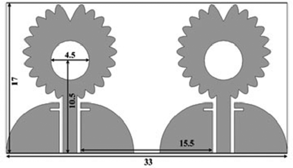
Fig. 1. Curved ground-based slotted feather-shaped monopole-based MIMO antenna arranged in spatial diversity mode [Reference Singhal60].
Advantages of this antenna are super wide bandwidth, good isolation, compact size, planar structure, and low cost. Spatial diversity configuration provides a bandwidth ratio of 11:1 at 4.4–51.5 GHz and isolation is >15 dB. The radiation pattern is bidirectional in E-plane and omnidirectional in H-plane. The envelope correlation coefficient (ECC), DG, and CCL are <−6 dB, 10 dB, and <0.4 b/s, respectively, which are suitable for MIMO applications. Limitations of this structure are low directivity, distorted pattern, and limited gain for 5G applications.
Another configuration is pattern diversity configuration in which two slotted feather-shaped monopole-based coplanar antennas are arranged orthogonally with a diagonal metallic strip-based decoupling structure to improve the isolation. Antenna geometry is shown in Fig. 2.
Fig. 2. Curved ground-based slotted feather-shaped monopole-based MIMO antenna arranged in pattern diversity mode [Reference Singhal60].
Strengths of this structure are super wide bandwidth, compact size, good MIMO performance, and improved isolation. The proposed structure is tuned between 3.8 and 51.5 GHz with a bandwidth of 171.2% and a bandwidth ratio of 13:1 which is greater than the previous configuration. Isolation is >15 dB at all operating frequencies except at 5 GHz.
Limitations of this structure are distorted radiation pattern, comparatively large size, and poor directivity for 5G application. Diversity performance is suitable as per the need of MIMO in the whole operating range.
Elliptical-shaped monopole antenna with coplanar waveguide and irregular ground plane
Coplanar waveguide-based elliptical monopole antenna with the defected ground plane is proposed in [Reference Rafique, Din and Khalil61]. Elliptical-shaped patch is fed by coplanar waveguide-tapered stripline with semi-ring. The antenna is fabricated on Rogers RT/Duroid 5880 substrate having a relative permittivity of 2.2 and a width of 1.57 mm and antenna geometry is depicted in Fig. 3.
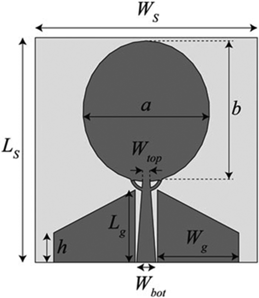
Fig. 3. Elliptical-shaped monopole with coplanar tapered waveguide and irregular ground plane [Reference Rafique, Din and Khalil61].
Firstly, the elliptical-shaped patch is fed by a conventional rectangular-shaped coplanar waveguide. The dimension of the elliptical-shaped patch can be calculated using the following formula:
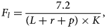
where Fl is the lower resonant frequency in GHz; L is the height of patch monopole; r is the equivalent radius of cylindrical monopole; p is the length of the microstrip feed line; K is the effective dielectric constant; the value of L for the elliptical patch can be given by L = 2 × A and r = 0.25 × B, where A is the semi-major axis length, B is the semi-minor axis length.
It is observed that elliptical-shaped monopole with a conventional coplanar waveguide with the rectangular ground is resonated from 3.1 to 11.3 GHz. Coplanar waveguide provides small losses, ease of fabrication, and co-planar behavior. When the elliptical-shaped patch is fed by tapered feed line and ground of triangular shaped with chopped corner is used, triband characteristics have been achieved between 1.27 GHz to 25 GHz. Tapered feed line provides good bandwidth and impedance-matching between feed and patch. Coplanar waveguide reduces the inductive effect of the patch by adding capacitance effect and forms purely resistive impedance. Two semi-rings are added at the connection between elliptical patch and tapered feed line. This technique increases bandwidth because multiple symmetrical feed lines allow vertical characteristics mode and effectively adjust vertical current distribution. In this way, bandwidth is enhanced and the antenna is resonated from 1.76 to 24.7 GHz.
Strengths of this antenna are planar structure, less complexity, low cost, and wide bandwidth. The limitation of this antenna is a large variation in gain over the whole operating frequency range, high cross-polar components due to thicker substrate than quarter wavelength, low gain of 3.8 dBi, and distorted radiation pattern. The efficiency of the antenna is 94.69% and radiation pattern is like the figure of eight in E-plane and omnidirectional in H-plane.
Slotted shovel-shaped patch antenna with symmetrically stair-shaped ground plane and coplanar waveguide feed
Compact super wideband-modified shovel-shaped monopole antenna with defected staircase coplanar ground is discussed in [Reference Dastranj, Lari and Bornapour62]. Initially, rectangular monopole antenna with conventional rectangular coplanar waveguide is designed which provides narrow band performance. In place of the rectangular patch, a shovel-shaped patch is designed. Bandwidth is increased but multiband characteristics are obtained between 2.8 and 40 GHz. When staircase ground is used with the shovel-shaped patch, then staircase ground decreases the leakage current distribution and enhances matching. There is an enhancement in bandwidth and improvement in impedance-matching when leaky wave interaction between the ground plane and the radiating patch is reduced. A C-shaped slot is cut from the patch to get band-stop characteristics for WiMAX band (3.7–4.7 GHz). Another C-shaped slot of lower size is etched from the patch and band gap characteristic was obtained for WLAN (5.7–6.4 GHz), circular slot is etched from the center. In this way, dual-band super wideband characteristic has been achieved. The motive of designing C-shaped slots is to eliminate the interferences of WiMAX and WLAN. The radius of the C-shaped slot decides the notch frequency range and lower radius will result in higher notch frequency. The proposed geometry is presented in Fig. 4 and an average gain of 2.96 dB was obtained. The radiation pattern is omnidirectional in H-plane and bidirectional in E-plane. Cross-polarization is small in low-frequency range while large in higher frequency range due to excitation of higher order modes.
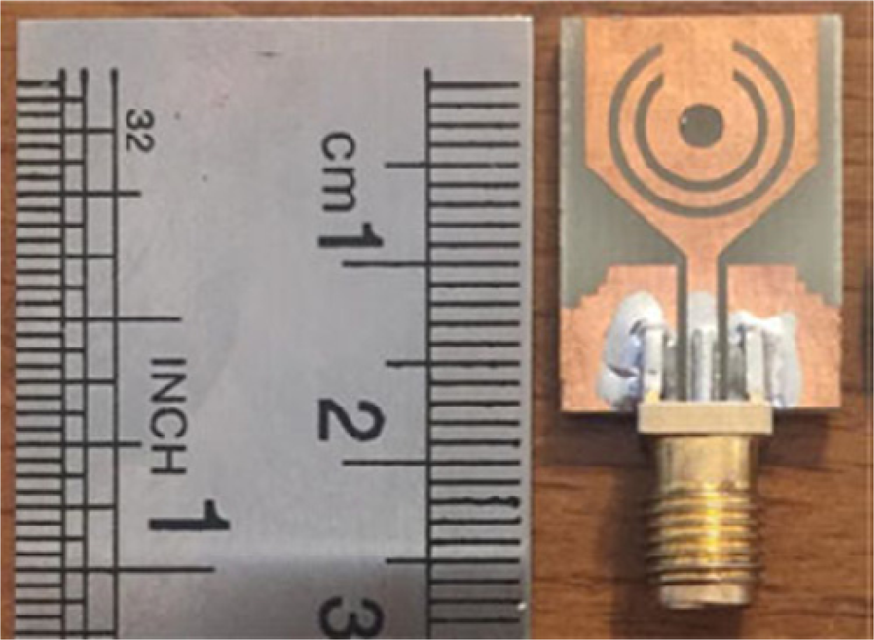
Fig. 4. Slotted shovel-shaped monopole with coplanar tapered waveguide and stair-shaped ground plane [Reference Dastranj, Lari and Bornapour62].
Strengths of this structure are compact size, super wideband characteristics, planar configuration, and controlled notch frequency. Limitations of this structure are large variation of gain over the operating frequency range, small gain, low directivity, high cross-polarization, and distorted radiation pattern.
Elliptically slotted inverted T-shaped sectored patch antenna array with defected ground plane
Four-element phased array of elliptically slotted inverted T-shaped sectored patch antenna with a defected ground plane is discussed in [Reference Anas, Shahid, Rauf and Shahid63]. Firstly, elliptical-shaped slot integrated with a rectangular slot is etched from a full metallic top layer of Rogers RO4533 substrate. The integrated semi-circular and conical-shaped patch is designed and fed with coplanar waveguide where microstripline is designed at the center for a single element. Inverted T-shaped stubs are added at the patch to achieve multiband operations and the notch is designed behind each stub to improve the return loss. Four curved-shaped slots are designed in the ground layer for a single element. These slots modify the current pattern and change the frequency of resonance due to the inductive effect of DGS. It changes resonant frequency by controlling electromagnetic wave propagation through the substrate. The diameter of the split ring, slot position, and slot width decide the resonant frequency. Four-element array is designed in this type of antenna. Spacing between array elements is 0.9λ to achieve good isolation and beam steering range. The top layer is shown in Fig. 5(c). Two four-element arrays are placed at the top and bottom side of PCB of the mobile layer as shown in Figs 5(a) and 5(b), respectively. Wide bandwidth is obtained due to elliptical-shaped slot aperture, stubs, and defected ground plane, and high gain is achieved using array configuration. The antenna is tuned at 28, 43, 51, and 64 GHz with the bandwidths of 3.9, 4, 3.9, and 11.8 GHz, respectively. If DGS is replaced by conventional ground, then the antenna is tuned at three frequencies. A total bandwidth of 23.6 GHz is obtained with DGS and 19.6 GHz without DGS. Single element provides a gain of 6–9 dBi in the operating frequency range while array provides a gain of 12–16.5 dBi in the operating frequency range. The radiation pattern of a single element is omnidirectional while it is directional with narrow beamwidth for the array. To steer the main beam, the phase shift between two elements is given according to the following formula:

where θ is the angle of the main beam; d is inter-element spacing, and λ is the wavelength.
Fig. 5. Elliptically slotted inverted T-shaped sectored patch antenna array with defected ground plane [Reference Anas, Shahid, Rauf and Shahid63] (a) Two 1 × 4 arrays at the top and bottom of mobile phone. (b) Back layer of mobile phone PCB, (c) top view of 1 × 4 array.
Beam is steered from −30 to 30° but scan loss and side lobe levels are high.
Major strengths of this structure are compact size, planar structure, good gain, multiband characteristics, and wide bandwidth. Limitations are high scan loss, high side lobe levels, and limited scanning range.
ME dipole antenna array on LTCC
Dual-polarized wideband magneto-electric dipole array is proposed in [Reference Li, Wang and Guo64]. Low temperature co-fired ceramic (LTCC) technology is used which provides ease of realizing multilayer structure. Four square patches constructed on the ceramic substrate are connected with the ground using vias and series of LTCC laminates. These patches create the pair of dipoles in the horizontal plane. Two perpendicular L-shaped probes are connected with microstriplines. It effectively excites dual-polarized radiation and acts as feed. Two microstriplines at the bottom deliver power to probes. Two parallel feeding networks are combined and used for excitation which consists of tapered microstriplines. Ferro-A6M ceramic laminate is used having dielectric constant, loss tangent, and thickness as 5.9, 0.002, and 0.096 mm, respectively. In this way, shorted patches behave like electromagnetic dipole by using the combination of vertical structure and ground. The resonant frequency of the antenna depends on the size of the patch and height of the patch. The dimensions of the L-shaped probe are responsible for the impedance-matching. A single structure provides 42.5% of bandwidth at 33.6 GHz and isolation is <−24 dB in the whole operating range. Isolation can be improved by adjusting the vertical distance of horizontal strips. The gain of the single antenna is 6.9 dBi with very small variation over bandwidth. Radiation pattern in E-plane is equal to the radiation pattern in H-plane. The radiation of vertical and horizontal polarization is also identical.
The 4 × 4 array of a previously discussed single element is designed on LTCC. Element spacing in the x and y direction is 0.49 × free space wavelength. Mutual coupling depends on the inter-element spacing. Port 1 and port 2 are the input ports of the feeding network and generate horizontally and vertically polarized EM (electromagnetic) radiations. Tapered microstripline is used for enhancing impedance-matching between 50 and 100 Ω. There are two parts in the excitation network and first part combines the input ports of the four-element linear array in the x-direction. The input of four linear arrays are extended and combined with part 2 and input ports at the bottom are not suitable for the measurements, so microstrip to coplanar grounded waveguide transition is used in array designing. Two columns of metallic pins are used to eliminate the surface waves. Vertical section of the substrate-integrated coaxial line is created with an outer conductor which is formed using metallic rings and pins between microstripline and coplanar line.
The antenna array is tuned from 25.6 to 40.8 GHz with a bandwidth of 45% and a gain of 16.1 and 15.6 dBi is obtained in vertical and horizontal polarizations. Radiation efficiency is >70% and advantages of this geometry are wide bandwidth, stable gain, dual polarization, good isolation, and low cross-polarization levels. Limitations of this structure are complex geometry, multilayer non-planar structure, fabrication difficulty, high cost, and misalignment problem at mm-wave.
Fabry–Perot resonant antenna with PRS
Circularly polarized Fabry–Perot resonant antenna is presented in [Reference Hussain, Jeong, Park and Kim65]. An individual element of the array consists of corner cut patch, diagonally arranged rectangular slot, and superstrate. Geometry is shown in Figs 6(a) and 6(b) and corner cut patch and diagonal slot increase the axial ratio bandwidth and are responsible for circularly polarized radiations. Partial reflecting surface with half-wavelength width superstrate is put at half-wavelength height above the radiating layer. It increases gain, impedance bandwidth, and axial ratio bandwidth. Dielectric layer with a permittivity of 10.2 and thickness is used as partially reflecting surface (PRS) which is put above the radiating patch with foam sandwiched between these to maintain the gap between radiating layer and PRS. Radiating patch is offset fed by the K-type connector. Due to truncated corners and diagonal slot, two orthogonal modes of equal magnitude are excited simultaneously. Truncated rectangular patch antenna provides low impedance and axial ratio bandwidth. After etching diagonal slot, resonance is shifted to lower frequency because the slot provides an additional path to current flow and both impedance bandwidth and axial ratio bandwidth are increased. In the presence of PRS above half-wavelength spacing from radiating patch, both bandwidths are enhanced. The single antenna provides 27.6% of impedance bandwidth and 18.5% of axial ratio bandwidth with a gain of 14.1 dBic. Gain is increased by approximately twice in the presence of PRS compared to the antenna without PRS. This antenna provides symmetrical stable directional radiation pattern in both E- and H-plane in the whole operating frequency range. Left-hand circularly polarized radiation is small compared to right-hand circularly polarized radiation (RHCP), so it provides RHCP radiation. The 2 × 2 MIMO array of Fabry–Perot antenna is designed as shown in Figs 6(c) and 6(d). Inter-element spacing is half of the free space wavelength. The designed antenna array is tuned from 25 to 33 GHz and provides a stable gain of 14.1 dB.
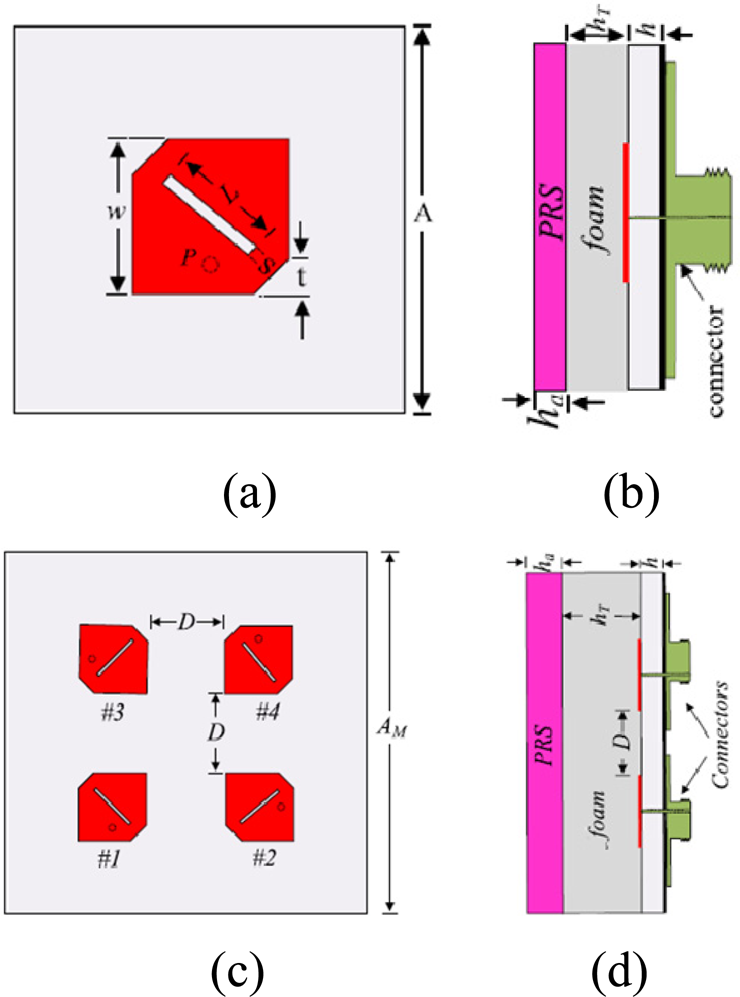
Fig. 6. Fabry–Perot resonant antenna with partially reflecting surface (PRS). (a) Single element top view, (b) single element side view, (c) array top view, (d) array side view [Reference Hussain, Jeong, Park and Kim65].
Strengths of this structure are wide impedance bandwidth and axial ratio bandwidth, circular polarization, improved isolation, good and stable gain over whole bandwidth, and limitation of this structure is its width.
Tapered slot ground antenna MIMO array
5G integrated along with 4G antenna is discussed in [Reference Al Abbas, Ikram, Mobashsher and Abbosh66] and a tapered slot is designed on the ground plane. Narrower edge of the slot is ended with a circular stub of a quarter of guided wavelength. Two microstriplines are designed on the top of the substrate and one microstripline (F2) is terminated with a circular-shaped sector. The geometry of the antenna is shown in Fig. 7 and the circular sector is connected with 50 Ω microstripline using a quarter wave transformer. Circular slot in ground plane and circular sector in stripline increase the bandwidth of the antenna. This stripline excites the slot at mm-wave frequency. Another microstripline consists of 50 Ω line, low-pass microstrip filter, and modified microstripline and it excites the slot in 4G band. Rogers RT/Duroid laminate with a dielectric constant of 2.2 is used. Low-pass filter is integrated with the structure to improve isolation and by properly feeding the antenna, it operates in two modes. When the slot is excited at the center, antenna works as tapered slot antenna and it provides end-fire radiation with high gain at mm-wave which is suitable for 5G. When the slot is excited at the corner, the antenna acts as an open-ended slot antenna and provides omnidirectional radiation for 4G at 2 GHz. If 4G feeder F1 is not added and 5G feeder F2 is excited, then propagation of current takes place toward the slot's open end. The antenna is tuned from 25 to 40 GHz with an approximate gain of 9.14 dBi. If 4G feeder is added without low-pass filter and modified stripline, the performance of antenna at mm-wave is degraded. Both gain and bandwidth decrease because 4G feeder acts as shunt impedance and blocks the signal propagation at 5G. Current is propagated toward the upper and lower side of 4G feeder and not propagated through an open-ended slot, isolation is also decreased. If narrow width transmission line which acts as shunt impedance is added with the 4G feeder, then shunt impedance of 4G feeder is increased and it behaves like an open circuit to mm-wave signal. Isolation is improved up to some extent using this and gain and bandwidth also increase. To improve the isolation between 4G and 5G feeder, stepped impedance-based low-pass filter with alternate low and high characteristics impedance line is added in 4G feeder. It improves isolation, gain, and bandwidth. To achieve MIMO characteristics, four antennas are arranged at four corners of the substrate and designed in spatial diversity mode. MIMO antenna operates from 25 to 40 GHz and 1.8 to 2.6 GHz. It provides the directional pattern with a gain of 7 dBi at mm-wave frequency and isotropic radiation pattern with a gain of 3 dBi at 2 GHz. The antenna delivers good MIMO performance and small users hand's effect on antenna.
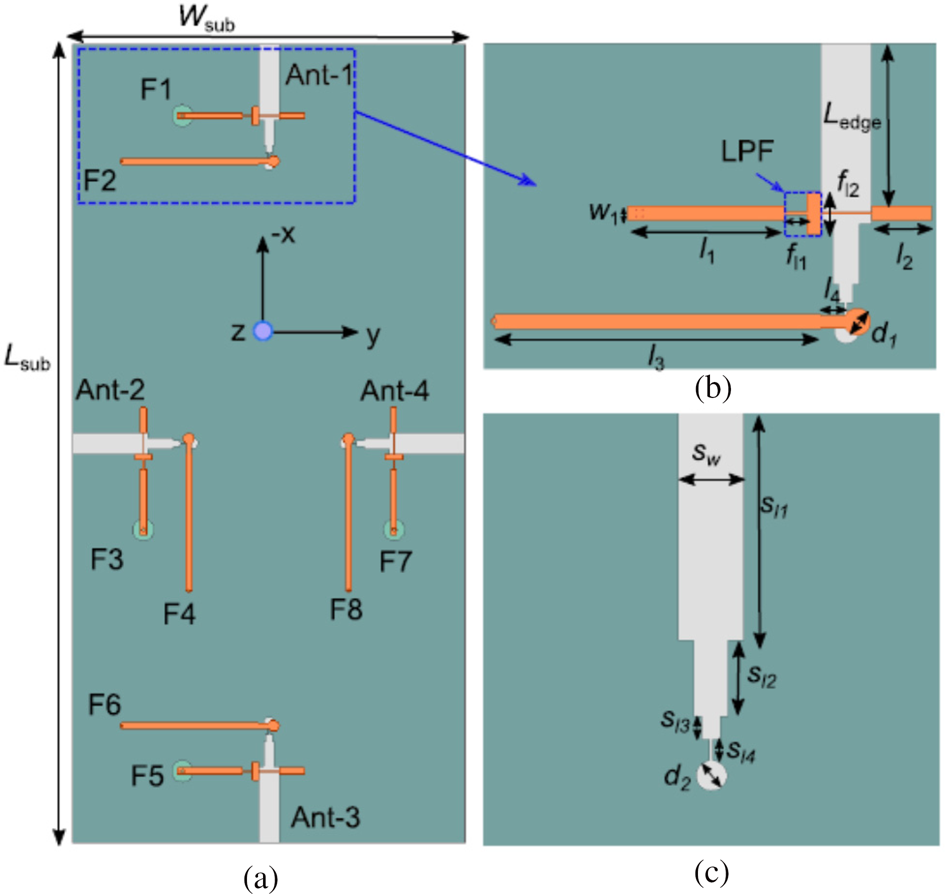
Fig. 7. Tapered slot ground antenna MIMO array. (a) MIMO antenna array, (b) individual antenna, (c) ground plane of individual antenna [Reference Al Abbas, Ikram, Mobashsher and Abbosh66].
Merits of this structure are good bandwidth, MIMO capability, planar structure, low user's hand effect, ease of mobile integration, and satisfying the requirement of 4G and 5G within the same aperture. Demerits of this structure are low gain, comparatively large size, inability to steer beam, high side lobe levels, and poor impedance-matching at 4G band.
Modified patch antenna with diagonal slot and metasurface
Circularly polarized, low profile, and wideband antenna is proposed in [Reference Hussain, Jeong, Abbas, Kim and Kim67]. Square patch with truncated corners and a diagonally rectangular slot is designed to achieve circular polarization and wide bandwidth. Metasurface is used above the patch without air gap for size miniaturization. Metasurface is two-dimensional equivalents of metamaterials which are used to reduce the size, increase gain, enhance axial ratio bandwidth, and get low profile structure. Metasurface consists of 4 × 4 array of symmetrical square rings with periodicity P. Gap between unit cell is termed as g. Patch and metasurface are printed on two different substrates with a dielectric constant of 2.2, a loss tangent of 0.0009, and a thickness of 0.51 mm. The patch is fed by 50 Ω K-type connector via microstripline, and to connect K-type connector with microstripline properly, a metallic pad is created. The geometry of the antenna is shown in Fig. 8.
Fig. 8. Modified patch antenna with diagonal slot and metasurface [Reference Hussain, Jeong, Abbas, Kim and Kim67]. (a) Side view, (b) metasurface, (c) top view.
When only truncated square patch is designed, the antenna is tuned from 26.9 to 28.4 GHz. Square antenna with a diagonal slot is resonated from 26 to 28.2 GHz with a reduced resonant frequency. When metasurface is stacked on the patch without air gap, the antenna provides 34.7% impedance bandwidth with frequency ranging from 24 to 34.1 GHz and a gain of 11 dBic along with circular polarization. Bandwidth is increased due to metasurface because it provides additional resonance when surface wave propagates through it. The antenna provides symmetrical and stable radiation pattern in both E- and H-plane and provides left-hand circular polarization. Strengths of this structure are wide bandwidth, stable radiation pattern, circular polarization, large axial ratio bandwidth, compact size, low profile, and ease of fabrication. Limitations of this structure are lower directivity and wide beamwidth and gain is also not sufficient to mitigate the losses of mm-wave band.
Printed quasi-Yagi diffraction grating-based antenna
High gain wideband quasi Yagi-Uda antenna with dielectric lens is reported in [Reference Mujammami and Sebak40]. The top layer of the antenna consists of a reflector, driven dipole, directors, and microstrip to slotline transition. U-shaped microstrip to slotline transition with balun is placed at the bottom layer to feed the dipole. This quasi-Yagi antenna excites dielectric slab waveguide. Tapered dipole and length of one effective wavelength are used in place of conventional dipole and half-wavelength to achieve wider bandwidth and high directivity, respectively. First director is placed at a distance of 0.1 × effective wavelength from the driven element. Second director is placed at a distance of 0.142 × effective wavelength from the first director. Multiple directors increase directivity as well as impedance-matching. Small spacing between elements increases the electromagnetic coupling due to surface wave and space wave in the substrate. Ground plane is placed at the back side with a distance of 0.25 × effective wavelength from the director which acts as a reflector. Ground plane has a width of 1.34 × effective wavelength. The antenna is designed in a particular way that its input impedance should be 50 Ω. U-shaped strip is used as balun (balance unbalance) structure and microstrip to slotline transition provides feeding to the quasi-Yagi antenna. Dielectric substrate acts as a dielectric lens but gain is degraded with unstable variations as the length is increased. Dielectric material has lossy behavior and there are total internal reflections for higher order modes which destructively interfere with propagating wave of fundamental mode and in this way gain reduces. To suppress undesired higher order modes, rectangular corrugations and holes are created in the dielectric slab waveguide, perpendicular to the direction of propagation or it is shaped as diffraction grating. It allows fundamental mode to propagate and suppress undesired higher order modes.
The wave is transmitted or reflected based on equation (3) of diffraction grating.

where G is groove per millimeters; m is the order of diffracted mode; n is the refractive index of the medium through which wave will transmit or reflect; ni is the refractive index of the medium that contains incident wave; θm is reflected or transmitted plane wave angle; θi is incident plane wave angle; λ is wavelength in incident region.
At a specific wavelength, all values of m satisfy:

where d = 1/G = corrugation period in mm.
It represents propagating diffraction order. If m = 0 then θo = −θi for all values of λ and it is the rule of reflection. Grating behaves like a mirror, so the wave is reflected and it is also called zero-order diffraction modes. This mode is used for designing high gain wideband end-fire mm-wave antenna. In dielectric slab waveguide with grating, wave is propagated in zero-order diffraction modes and eliminates higher order modes. Wave is guided through a corrugated dielectric slab substrate. The antenna is tuned from 24 to 40 GHz with a bandwidth of 40% at 28 GHz and the gain of the antenna is 14–15.1 dBi. Corrugated dielectric slab acts as band pass filter and cross-polarization is <−22 dB. Advantages of this structure are high gain, stable gain over bandwidth, low side lobe, and cross-polarization level, wide bandwidth, excellent impedance-matching, and good directivity. Limitations of this structure are complex geometry and large size.
Binary coding-stacked patch antenna
A dual-polarized broadband antenna is discussed in [Reference Wang, Geng, Wang, Zhou, Ren, Wu, Zhao, He, Liang, Zhu and Jin68]. The antenna has two binary coding-stacked patches. Binary coding patch implies that patch is made using an array of small rectangular patches which can be optimized by binary codes. There are two substrates of Arlon 250 having a dielectric constant of 2.5 and three metallic layers which are connected using vias. The top layer is the driven patch which is formed on the upper substrate. The middle layer is the parasitic patch which is formed on top of the bottom substrate. The lowest layer is the ground plane which is formed on the bottom of the lower substrate. The driven patch is fed using two SMA (SubMiniature version A) connectors which are placed at the bottom for this purpose. Two circular rings are added on the driven patch. Both patches consist of 10 × 10 grid array whose state is calculated by binary code. If code is 0, the grid is formed using air, and if code is 1, the grid is formed using metal. Binary code needs to be optimized for achieving broad bandwidth and high gain. Binary string is symmetrical along diameter in both of the patches. This coded pattern changes the phase of current passing through the patch.
The reported antenna is tuned from 21.8 to 33.2 GHz and a single element provides 5.8 dBi of gain. Eight-element linear array with an element spacing of 4.6 mm is designed to increase the gain. The array is excited using phase gradient delay line. The scanning range of array is ±50° at 30 GHz and gain fluctuation is <3 dB. The gain of array is between 9 and 11.45 dBi and strengths of this structure are wide impedance bandwidth, dual-polarization capability, high scanning range, low scanning loss, and good isolation. Limitation of this antenna is fabrication difficulty, higher thickness, and limited gain.
Amer fractal slot MIMO antenna
Wideband fractal slot antenna is presented in [Reference Abed Sahab and Jawad69]. Amer-shaped fractal slot is etched from radiating patch. The patch is fed by four feed lines which are placed at four sides. Ground plane is placed on the same plane so coplanar waveguide feeding is used. Antenna geometry is shown in Fig. 9. By optimizing the gaps near feeding line, leakage of electromagnetic energy can be controlled. The dimension of coplanar waveguide controls the impedance-matching and dimension d is chosen as 1 mm. When port 1 is excited, the antenna is tuned from 1.5 to 37 GHz. If port 2 is excited, the antenna is resonated from 1.35 to 36 GHz. If port 3 is excited, then the antenna is tuned from 1.3 to 30 GHz. If port 4 is excited, then the antenna is resonated at multiple bands from 1.5 to 10.3 GHz and 10.6 to 39.3 GHz. Bandwidth is increased due to multiple paths available for surface current in Amer fractal slot antenna. Each path creates individual resonance and antenna also provides circular polarized radiation, its gain varies from 1 to 6.3 dBi.
Fig. 9. Amer fractal slot MIMO antenna [Reference Abed Sahab and Jawad69].
Strengths of this structure are wide bandwidth, good isolation, circular polarization, compact, and planar geometry. Limitations are low gain, large variation in gain over operating frequency, and low directivity.
Characteristics of 5G antenna and performance enhancement techniques
5G antenna's radiation characteristics are very different from 4G and previous generation antennas. Earlier communication protocols and antenna characteristics are based on microwave frequencies which are needed to be moderated for 5G because of the use of mm-wave spectrum. The antennas used at 5G transceivers are required to provide and establish the secure wireless link with reliable communication to support Gbps (giga-bit-per-second) speed. Traditional antennas broadcast radiation in all directions so the connection can be established in any direction but 5G antennas will not broadcast. 5G antennas will radiate at a specific direction and need to communicate with several users simultaneously. If intended user is at 0° at some time and after a minute if it is moved to 40° with respect to the antenna, then the antenna is required to direct the main beam at 40° and nulls at 0°. The antenna should dynamically change its characteristics based on the mobility of the user. It is not only challenging to design but also difficult to test because everything is in motion [Reference Andrews, Buzzi, Choi, Hanly, Lozano, Soong and Zhang4, Reference Hong, Baek, Lee, Kim and Ko5]. Although we have done a comprehensive survey of bandwidth enhancement techniques in this work, a brief description of other important radiation performance parameters for 5G communication is provided below:
High gain
At mm-wave, environmental losses and link losses are high. To mitigate these losses, high gain antenna and line of sight communication are required [Reference Hong, Baek, Lee, Kim and Ko5]. Various techniques have been reported in the literature to increase the gain. Some reported gain enhancement techniques used in 5G antennas are designing of array [Reference Hong, Baek, Lee, Kim and Ko5, Reference Khalily, Tafazoll, Xiao and Kishk8–Reference Ojaroudiparchin, Shen, Zhang and Pedersen11], printed Yagi-Uda antenna [Reference Mantash and Denidni14], replacement of Artificial Magnetic Conductor (AMC) in place of perfect electric conductor ground [Reference Mantash and Denidni14], placement of anisotropic metasurface at aperture [Reference Zhu, Liu and Wen15], stacking of dielectric superstrate above antenna [Reference Haraz, Elboushi, Alshebeili and Sebak23], modified BM cascaded with microstrip combline array [Reference Trinh-Van, Lee, Yang, Lee and Hwang32], addition of semi-ring-shaped DGS at edges [Reference Zhu, Liu, Wen, Chen and Xu52], clover-like conductor profile [Reference Ozpinar, Aksimsek and Tokan39], quasi-Yagi antenna array with ladder-like director [Reference Mujammami and Sebak40, Reference Mujammami and Sebak40], Fermi antenna [Reference Phala, Briquech and Sebak42], Vivaldi antenna array [Reference Zhu, Liu, Wen, Chen and Xu52], dielectric lens [Reference Zhu, Liu and Wen15], inductive windows in SIW power divider [Reference Zhu, Liu, Wen, Chen and Xu52], electromagnetic band gap (EBG) [Reference Zhu, Liu, Wen, Chen and Xu52], extension of ground in inverted U-shape [Reference Ullah and Tahir54], dielectric rods [Reference Zhu, Liu and Wen15], triangular director [Reference Zhu, Liu and Wen15], etc.
Narrow beam steerable radiation pattern
To maintain the line of sight communication with a mobile user, a steerable narrow beam radiation pattern is required. Numerous methods reported in the literature for beam switching are phased array with electronic switching [Reference Andrews, Buzzi, Choi, Hanly, Lozano, Soong and Zhang4], mechanical beam steering [Reference Andrews, Buzzi, Choi, Hanly, Lozano, Soong and Zhang4], EBG material [Reference Zhu, Liu, Wen, Chen and Xu52], periodic structures such as high impedance surface [Reference Mantash and Denidni14], frequency-selective surface [Reference Mantash and Denidni14], AMC [Reference Mantash and Denidni14], split-ring resonator [Reference Shen, Liu, Zhao, Huang, Shi and Huang53], tunable impedance surface with vias [Reference Mantash and Denidni14], multiple varactor diodes [Reference Hong, Baek, Lee, Kim and Ko5], RF MEMS switches [Reference Hong, Baek, Lee, Kim and Ko5], PIN diodes [Reference Hong, Baek, Lee, Kim and Ko5], etc.
Low side lobe levels
For a wide range of beam steering, side lobe levels must be very low and beamwidth should be small [Reference Hong, Baek, Lee, Kim and Ko5]. At higher scan angles, maintaining low side lobe levels and narrow beamwidth is very challenging for designers [Reference Roh, Seol, Park, Lee, Lee, Kim, Cho, Cheun and Aryanfar6]. Several practices have been described in the literature to reduce side lobe levels, non-uniform amplitude excitation in phased array [Reference Trinh-Van, Lee, Yang, Lee and Hwang32], alternative 180° rotated array [Reference Khalily, Tafazoll, Xiao and Kishk8], unequal split power divider with BM [Reference Trinh-Van, Lee, Yang, Lee and Hwang32], tapered amplitude distribution [Reference Trinh-Van, Lee, Yang, Lee and Hwang32], Taylor beam forming distribution [Reference Ullah and Tahir54], etc.
Low specific absorption rate
For 5G mobile antenna, specific absorption rate (SAR) should be <1.6 Watt/kg for the human body as per the guidelines of FCC [Reference Geyikoğlu, Koç Polat, Kaburcuk and Çavuşoğlu71]. SAR is the amount of electromagnetic energy absorbed by the unit mass of human tissue. SAR can be reduced by properly selecting the position of the antenna in the phone, using ferrite sheet, metamaterials, EBG, etc. [Reference Hong, Baek, Lee, Kim and Ko5]. For mobile antenna, the position of the antenna should be carefully decided so that it can efficiently work along with other components such as LCD, battery, metallic back casing, and other antennas for Wi-Fi and Bluetooth [Reference Khalily, Tafazoll, Xiao and Kishk8]. SAR can be reduced by properly selecting the position of antennas in the mobile phone.
Good isolation
To increase the system capacity, spectral efficiency, data throughput, and reduced effects of multipath interference, massive MIMO antenna system is used in the 5G. Massive MIMO system consists of a large number of antennas at transmitter and receiver which provide multiple data links for communication simultaneously on the same radio channel. Three concepts such as spatial diversity, spatial multiplexing, and beamforming are involved in MIMO. Spatial diversity improves the system reliability in which the same data are propagated through multiple paths or links or spatial. Multiple messages can be simultaneously transmitted and received between transmitter and receiver in spatial multiplexing. Using beamforming technique, antenna systems at transmitter and receiver transmit or receive the signal in a specific direction rather than sending or receiving or broadcasting in all directions. For reducing the size of the antenna system and to meet the space requirements at mobile stations and base stations, it is required to optimize the isolation and use proper decoupling techniques. Polarization diversity and good isolation can be achieved using the optimized arrangement of linearly polarized antennas [Reference Yang78]. Some of the techniques reported in the literature for 5G antennas which provides good isolation, are alternate 180° rotated and alternate phased feed lines [Reference Khalily, Tafazoll, Xiao and Kishk8], using EBG materials at specific positions [Reference Griguer, Marzolf, Lalj, Riouch and Drissi18, Reference Christie, Cahill, Buchanan, Fusco, Mitchell, Munro and Maxwell-Cox33], employing H-shaped slots between antenna elements, using line-type defected ground system between antennas [Reference Jang21], orthogonal polarization, quasi-Yagi antenna [Reference Mujammami and Sebak40, Reference Zeng and Luk41], neutralization line, dielectric directors [Reference Christie, Cahill, Buchanan, Fusco, Mitchell, Munro and Maxwell-Cox33], metasurface corrugations [Reference Griguer, Marzolf, Lalj, Riouch and Drissi18], double-layer CSRRs [Reference Alizadeh, Ghobadi, Nourinia and Zayer77], EBG ground [Reference Zhu, Liu, Wen, Chen and Xu52], split-ring resonators [Reference Singhal and Budania49], coupled resonators [Reference Singhal and Budania49], Fermi antenna [Reference Phala, Briquech and Sebak42], DGS, unequal E-shaped stubs [Reference Djerafi, Fonseca and Wu36], Vivaldi antenna [Reference Zhu, Liu and Wen15], decoupling elements, self-isolated antennas [Reference Yang78, Reference Zhao and Ren79], dual-polarized elements, and many more.
Compact size
For 5G mobile stations, compact antenna is preferred because of the availability of limited space. Each antenna size should be at least a quarter of guided wavelength to achieve good radiation efficiency and reduce stored energy in near-field regions. PCB thickness of a cellular phone is mostly about <1 mm. Thicker PCB increases the production cost in consumer electronics. To meet the space requirements of 5G mobile stations, some of the reported techniques are four CSRRs in the ground [Reference Alizadeh, Ghobadi, Nourinia and Zayer77], anisotropic metasurface [Reference Griguer, Marzolf, Lalj, Riouch and Drissi18], direct feed structures, EBG ground, two closely proximate E-shaped microstrip antenna, and many more [Reference Yassin, Mohamed, Abdallah and El-Hennawy12, Reference Vashist, Soni and Singhal34, Reference Yang78].
MIMO parameters
MIMO antennas are popularly used in the 5G to mitigate the effects of multipath propagation, increasing the capacity and spectral efficiency. The performance of MIMO antennas is analyzed using some additional parameters such as TARC, CCL, MEG, ECC, and DG.
TARC is calculated using a scattering matrix. It is the ratio of the square root of total output power at the ports to the square root of total incoming powers. It depends on the frequency, scan angle, and tapering. It characterizes the frequency bandwidth and radiation performance of MIMO systems. TARC should be zero or less which represents efficient radiation of all the power and least unwanted reflected power.
Another parameter is CCL. CCL represents transmission loss in bits/sec/hertz. It represents the limit up to which lossless communication is done. It should be <0.4 bits/sec/hertz.
MEG quantifies reception ability of antenna in the multipath environment. It can be calculated by the ratio of mean output power to mean input power. It can be calculated by taking the ratio of power received by the antenna to power received by the isotropic antenna in the fading environment. It should be <3 dB and represents effective diversity performance.
ECC represents the ability to radiate independently of two antennas. If one antenna is horizontally polarized and another antenna is vertically polarized, then ECC is zero. ECC should be <0.5. It can be calculated using a scattering matrix.
Another one is DG which represents an improvement in the signal-to-noise ratio of the multiple antenna system. DG should be ideally equal to 10. All these MIMO parameters can be calculated using a scattering matrix [Reference Rubani, Gupta and Rajawat50].
Low cross-polarization
When the size of the antenna is small, cross-polarization and isolation are needed to be analyzed carefully. High cross-polarization creates distortion in the signal quality of communication [Reference Mohsen, Isa, Isa, Abdulhameed, Attiah and Dinar30]. Low cross-polarization level improves the polarization purity and isolation. Various techniques can be used to reduce cross-polarization levels which are dielectric resonator antenna, differential feeding method, complementary structure [Reference Feng, Luo, Zhou and Sim80], DGS, dot and arc-shaped DGS, L-shaped DGS, metal wall, split-ring resonator, anisotropic metasurface [Reference Shi, Zhu, Li, Zhang and Xu81], metamaterial mushroom, L-probe fed patch, cavity-backed slot [Reference Yin, Wu, Yu, Wang and Hong17], DD patch array antenna [Reference Lee, Luk, Tong, Shum, Huynh and Lee19], balanced symmetric structure [Reference Mohsen, Isa, Isa, Abdulhameed, Attiah and Dinar30], and many more.
Performance comparison of various structures
Performance comparison of various wideband antennas is shown in Table 1. To support giga-bit-per-second data rate, wideband mm-wave antenna is required in the 5G communication, but along with wide bandwidth performance, other characteristics such as moderate gain, narrow beamwidth, and steerable characteristics are also required to mitigate the link losses and environmental losses experienced at mm-wave. It may be noted that monopole antenna with defected ground plane and coplanar waveguide provides excellent super wideband operations. Structures proposed in [Reference Singhal60–Reference Anas, Shahid, Rauf and Shahid63] provide impedance bandwidth >160%. This technique also provides compact, planar, and low-cost structure but gain is very small in the range of 2–3 dBi. Distorted radiation pattern, large variations in the gain over frequencies are the major limitations. Quasi-Yagi antenna with dielectric lens [Reference Mujammami and Sebak40], Fabry–Perot resonant antenna [Reference Hussain, Jeong, Park and Kim65], and metamaterial-based antenna provide good stability of gain over bandwidth but bandwidth is not as much enhanced as the monopole antenna with DGS. Size and volume of the antenna are increased in [Reference Mujammami and Sebak40] and [Reference Wang, Geng, Wang, Zhou, Ren, Wu, Zhao, He, Liang, Zhu and Jin68] but metamaterial-based structure [Reference Hussain, Jeong, Abbas, Kim and Kim67] provides a good reduction in size with improved isolation. Amer fractal slot MIMO antenna with coplanar waveguide [Reference Abed Sahab and Jawad69] provides wide bandwidth along with good gain and compact size. Good impedance bandwidth along with large axial ratio bandwidth is achieved in [Reference Hussain, Jeong, Park and Kim65] and [Reference Hussain, Jeong, Abbas, Kim and Kim67]. Diagonal slot and truncated square patch improve axial ratio bandwidth along with impedance bandwidth. The structure discussed in [Reference Wang, Geng, Wang, Zhou, Ren, Wu, Zhao, He, Liang, Zhu and Jin68] provides good steerable characteristics along with improved gain and bandwidth. MIMO capability is also required to improve the signal-to-noise ratio and the capacity which is presented in [Reference Singhal60, Reference Al Abbas, Ikram, Mobashsher and Abbosh66, Reference Abed Sahab and Jawad69]. To satisfy the bandwidth requirement of 5G, the antenna should provide not only wide bandwidth but also satisfy other factors such as high gain, pattern stability, compact size, low side lobe levels, reduced mutual coupling, and low cross-polarization is needed to consider and optimize.
Table 1. Performance comparisons of various antennas used for 5G
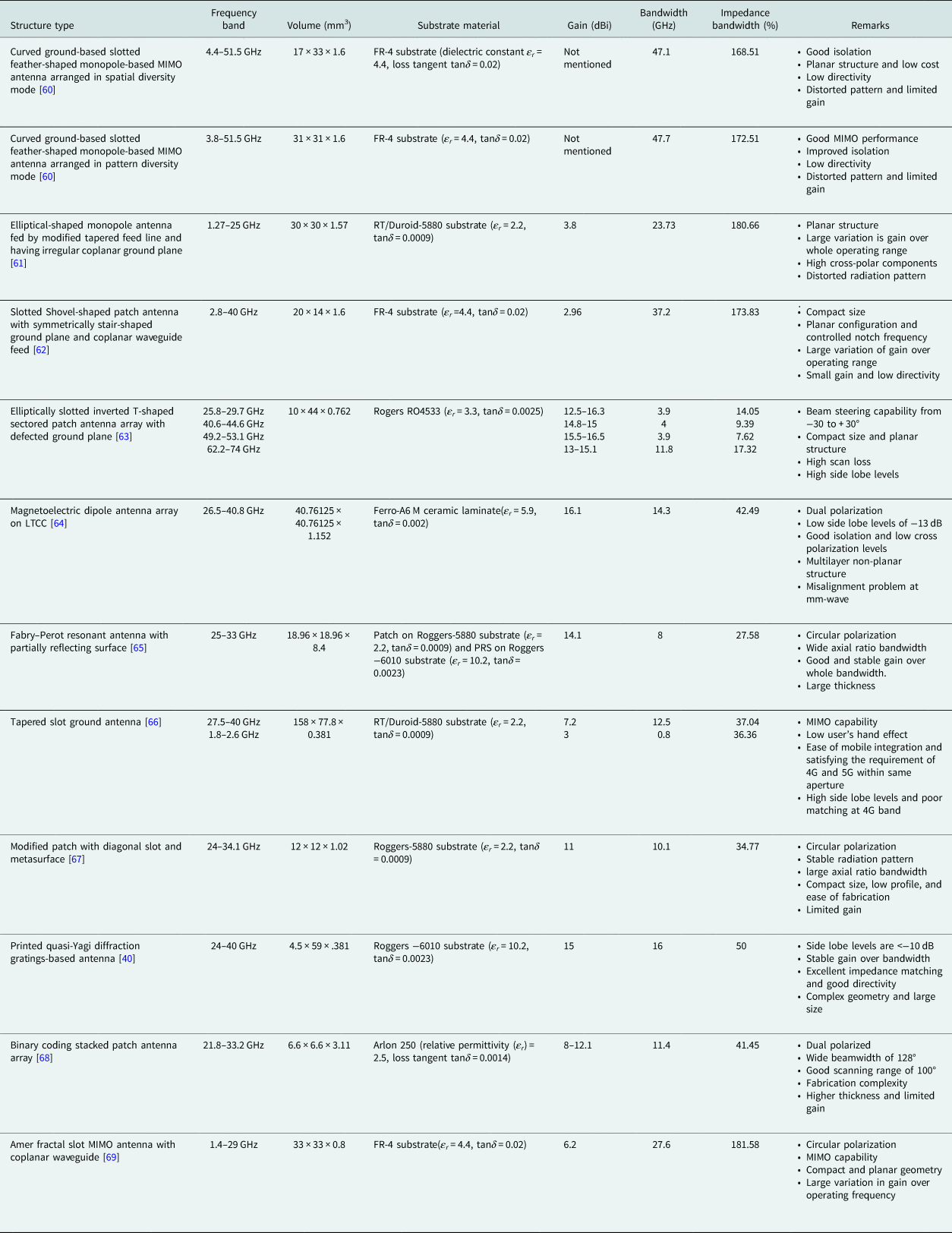
Conclusion
The antenna is a very important component of wireless communication and its performance decides the efficient utilization of RF energy. Currently, microstrip antennas are mostly used due to its small size, low cost, ease of fabrication, multiband capability, and ability to generate various polarized signals but its limitations are narrow bandwidth, limited gain, polarization impurity, and low efficiency. Researchers have reported various techniques in the literature to improve bandwidth, gain, and efficiency but most of the techniques have been proposed for microwave antennas. Due to bandwidth shortage at sub 6 GHz band or microwave band, mm-wave band will be utilized in future wireless communication which has large available bandwidth. Due to a small wavelength of mm-wave, it experiences large link losses and environmental losses. Antenna with not only wide bandwidth but also highly directional and high gain characteristics will be utilized to mitigate the environmental effects and losses of mm-wave. Traditional bandwidth enhancement techniques are needed to utilize along with advanced technologies. Various bandwidth enhancement techniques used for 5G mm-wave antennas are discussed in this paper along with their strengths and limitations. Traditional techniques to improve bandwidth are designing slots of various shapes, electromagnetic coupled and proximity coupled feeding techniques, impedance-matching techniques, stacked configuration, modified substrates, coplanar parasitic elements, defected ground, etc. It is very challenging to achieve stable gain and radiation pattern over the whole operating range, compact size, planar configuration, narrow beamwidth, and low side lobe levels along with bandwidth enhancement. Various techniques such as tapered slot antenna, metamaterial-based antenna, vertical resonant coupled structure, stubs and curved ground, curved dipoles, EBG structures, wideband beamforming networks such as Blass matrix and Buttler matrix, dielectric lens, leaky wave antenna, coplanar waveguide, monopole configuration electromagnetic dipole, etc., may be used for mm-wave antennas. Combination of various techniques may be utilized for bandwidth enhancement along with solving the afore-mentioned problem.
 Tapan Nahar is presently a Ph.D. scholar in Electronics and Communication Engineering Department, Manipal University Jaipur, India. He graduated with the Bachelor of Engineering (BE) degree in Electronics and Communication from the Global Institute of Technology, Jaipur in 2009. He did the M.Tech degree in Digital Communication from the Poornima College of Engineering, Jaipur in 2015. He has many years of experience in teaching to undergraduate disciplines. He is pursuing the Ph.D. degree in the research area of planar antennas for 5G mobile technology. He has to his credit several technical papers in international and national conferences and books on various subjects.
 Dr. Sanyog Rawat is presently associated with Electronics and Communication Engineering Department, Manipal University Jaipur. He has been into teaching and research for more than 16 years. He graduated with the Bachelor of Engineering (B.E.) degree in Electronics and Communication, the Master of Technology (M.Tech) degree in Microwave Engineering, and the Ph.D. degree in the field of Planar Antennas. Dr. Rawat has been engaged actively in the research areas and published more than 80 research papers in peer-reviewed international journals, book series, and IEEE/Springer conferences. He has organized several workshops, seminars, national, and international conferences. He has been empaneled in the editorial board of various national and international journals. He has supervised nearly 30 M.Tech dissertations and three Ph.D. scholars, and is guiding six scholars for Ph.D. His current research interests include reconfigurable RF-printed circuits, passive and active microwave-integrated circuits. He has visited countries such as Japan, Thailand, Malaysia, UAE, and Indonesia for academic and research work. He is also a member of several academic and professional bodies, i.e. Senior Member IEEE, Member IE and ISLE.


