I. INTRODUCTION
Integrated frequency-modulated-continuous-wave (FMCW) radar transmitters and receivers at 24 GHz and higher frequencies have been the focus of the many recent studies [Reference Forstner and Knapp1–Reference Krishnaswamy and Hashemi13]. A fully integrated transceiver, which integrates all radio frequency (RF) and microwave components, has great advantages in terms of cost, system integrity, RF signal cross-talk, and transmission loss as well as the overall power consumption. These advantages especially become more prominent at higher operational frequencies.
Traditionally, III–V processes as well as SiGe technologies are utilized for the transceiver's implementations, operating at these frequencies [Reference Forstner and Knapp1–Reference Jain, Tzeng, Zhou and Heydari4]. However, in recent years, CMOS technologies are becoming more favorable as the rapid downscaling of CMOS processes allows the designers to implement their circuits on these technologies with less production cost and better analog–digital integrity [Reference Saunders5–Reference Li, Hung, Huang and Lee8].
In this work, a 24 GHz low-power FMCW secondary radar transceiver, targeted for wireless localization [Reference Vossiek, Wiebking, Gulden, Wieghardt, Hoffmann and Heide14, Reference Roehr, Gulden and Vossiek15] is designed and fabricated using the 130 nm CMOS technology. The 130 nm CMOS process has a cut-off frequency of 90 GHz which is suitable for radar systems operating at 24 GHz. The realized microchip has been measured for further verification of the design. The transceiver includes a local-oscillator (LO) generator, a transmitter and four receiver front-ends. It has two receiving modes and a transmitter mode through a switching technique, which is implemented in the LO and direct-current (DC) paths. Compared with the traditional multi-channel receiving (MCR) mode, the introduced switch-channel receiving mode (SCR) has better noise performance and consumes less power. With four receiver front-ends, a receiving antenna array can be implemented and an angle-of-arrival (AOA)-based localization can be realized [Reference Lee and Kim16]. By combining time-difference of arrival and AOA techniques, the accuracy of the wireless localization can be improved.
The paper is organized as follows. In Section II, the implemented transceiver architecture will be presented. Section III discusses the design of different building blocks, including the receivers, the transmitter, and the LO generations circuits. Section IV discusses the integration considerations of the full transceiver chip. Section V shows the simulation and measurement results. Section VI concludes this paper.
II. TRANSCEIVER ARCHITECTURE
Figure 1 shows the block diagram of the designed switch-channel FMCW transceiver. The voltage controlled oscillator (VCO) is modulated by an external control signal and generates the FMCW signal at 24 GHz. The output signals of the VCO are amplified by two buffers. One output signal is converted to differential signal by a balun, and then divided by 8 through a frequency divider. The 3 GHz output signal is send to the external phase-locked loop (PLL). The other output of VCO is sent through the power division circuitries to the receiver and transmitter front-ends.

Fig. 1. Block diagram of the designed switch-channel transceiver.
The transmitter comprises a buffer amplifier and a power amplifier, while the receiver includes an low noise amplifier (LNA), an intermediate frequency (IF) amplifier, a mixer and a transformer balun. In transmitting mode, the VCO signal is firstly amplified by the buffer amplifier, and eventually amplified by the power amplifier (PA) while in the receiver, firstly the received and filtered signal is amplified by the LNA and then down converted to the low IF through a passive mixer.
As mentioned before, through the LO switching and biasing control, two receiving modes are available. In MCR mode, all the receiver channels are turned on at the same time. The LO signals are distributed equally into the four channels. This mode enables AOA-based localization by introducing an antenna array. However, the power consumption is considerably high as four channels operate at the same time. The channel-to-channel cross-talk could also deteriorate the receiver performance.
In SCR mode, the receiver channels are switched on and off one by one. As each the receiver is connected to an antenna array unit, by analyzing the received signals at different channels, AOA-based localization can be realized. Compared with the switch-antenna receivers [Reference Lee and Kim16], this transceiver does not require a single-pole-four-throw RF switch at the receiver input; hence the noise figure of this receiver is much lower than the switch-antenna receivers. Additionally, multiple receivers provide redundancy for the radar system.
Compared with the MCR mode, the SCR mode has the following advantages. Firstly, the power consumption is much lower as only one receiver channel is switched on at any time. Secondly, there is no channel-to-channel cross-talk in SCR mode. Thirdly, all LO power are sent to the operating receiver, therefore the gain, linearity, and noise figure of the receiver channel are improved. However, SCR mode brings some complexity to the baseband signal processing.
In this work, before starting with circuit designs, the link budget has been calculated. The calculations have been performed for the worst case scenarios at the maximum range of 50 m distance and single receiver channel. Based on the baseband circuitry requirements, the required SNR at the output of the receiver should be higher than 15 dB. By assuming less than 7 dB noise figure (NF) for the RX and 14 dBi antenna gain in both TX and RX paths, the required TX output power of 0 dBm is calculated. Such a low output power requirement can be totally achieved with an efficient PA on this technology. Also, the initial NF value in this design has been selected based on the so far published state-of-the-art results [Reference Issakov6, Reference Guan and Hajimiri9]. Further, by designing higher power PAs, the NF requirement can be eased.
The CMOS process used for the transceiver design is IBM 8RF 0.13 µm CMOS process. RF n-channel metal-oxide-semiconductor (NMOS) transistors in this process have a cut-off frequency of 90 GHz, which is quite suitable for 24 GHz design. To optimize the circuit performance, the finger lengths of the RF transistors are set to 0.13 µm in the transceiver.
III. CIRCUIT BLOCKS
In this section the detailed design of each component is explained. Starting from the transistor size optimization until the final circuit integration a very systematic design procedure has been followed [Reference Subramanian, Jamal Deen and Boeck17]. The design of the key components in LO generation circuits, the transmitter and receivers are discussed below.
A) LO generation circuits
LO signal is generated by VCO, amplified by buffers, and controlled by switches. The design of the divider is similar to the one presented in [Reference Shu, Subramanian and Boeck18] and hence its details are not presented in this work.
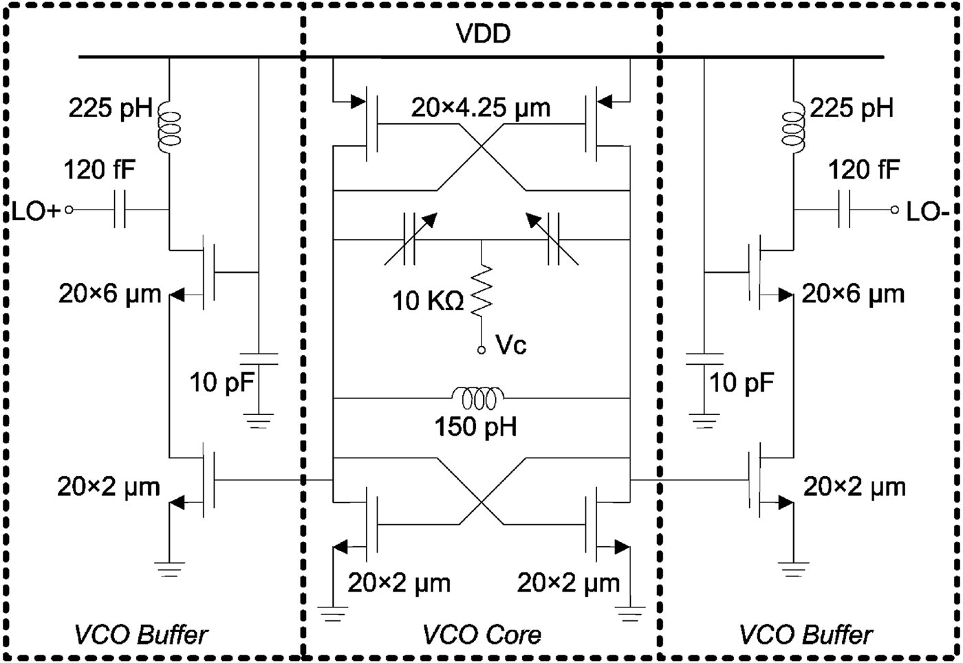
As VCO defines the operating frequency and the phase noise (PN) of the transceiver system, it is one of the most critical circuit blocks. Figure 2 shows the schematic of the designed VCO with PMOS (p-channel metal-oxide-semiconductor transistor)/NMOS cross-coupled topology. The VCO is self-biased as current source transistors could bring additional PN to the VCO. The NMOS transistors have widths of 20 × 2 µm, whereas the PMOS transistors have widths of 20 × 4.25 µm as the transconductance is similar to NMOS. The transistor sizes are optimized for minimum supply current and PN. The tank circuit consists of two parallel varactors and one inductor. The one-turn 150 pH inductor is designed with patterned ground shielding to avoid substrate coupling and the NMOS varactors are selected with minimum channel length for minimum PN degradation. The control voltage Vc is connected to the center of the symmetrically connected varactors.
Fig. 2. VCO schematic.
Two buffers with cascode topology are implemented to amplify the VCO output and to isolate the VCO core from the loading circuits. Compared with the widely used common-drain buffers, the cascode topology provides much higher reverse isolation and higher gain. The reverse isolation is very important at 24 GHz as the VCO core is very sensitive to the external loading. The impedance of the loading circuits varies as the transceiver switches between transmitting and receiving modes. If the isolation is not maximized, the VCO output frequency would be pulled by the load impedances. The cascode topology shows approximately 30 dB isolation in the simulation. The transconductance transistor size is set to 20 × 2 µm, whereas the cascode transistor size is set to 20 × 6 µm. The LO output is matched to 50 Ω using a LC matching network.
The layout of the VCO and buffers are carefully performed as the VCO oscillation frequency is very sensitive to parasitic effects of the interconnect lines. The layout is highly integrated. The interconnection lines are set as short as possible while keeping a certain distance between the inductors for minimized mutual coupling. Triple well NMOS transistors are implemented to reduce the substrate coupling. The layout is EM-modeled using ADS Momentum. The inductor and varactors are modified to center at the oscillation frequency at 24 GHz.
The LO output of one buffer is sent to a passive LO power distribution circuit. The circuit is based on 50 Ω side-shielded microstrip lines on top metal with 5 µm width. These microstrip lines have little insertion loss, while the side-shield limits the mutual coupling between adjacent transmission lines. To ensure the LO power being distributed equally into the four receiver channels, the circuit is laid out highly symmetrical for all four receiver outputs. To reduce the loss of the LO signal at thetransmitter input, a straight transmission line is implemented to connect the VCO buffer and the transmitter. The distances between different branches of the power distribution circuit are set as 100 µm to avoid the cross-talk between different channels.
To further enhance the LO power at different modes, the LO output from the power distribution circuit is controlled by TX and RX LO switches. At TX mode, the TX LO switch is turned on and the RX LO switches are turned off; therefore, the LO signal is send to the TX through a straight transmission line. At MCR mode, the RX LO switches are turned on and the TX LO switch is turned off, hence the LO signal is equally distributed into the four RX channels. At SCR mode, for a certain time, one RX switch is turned on and other switches are turned off; therefore, the LO signal is send to a certain RX channel.
The LO signal available at receiver LO input at SCR mode is 6 dB higher than that of the MCR mode. High LO level brings a lot of advantages, such as improved linearity, gain and noise performance. Besides, SCR mode does not require additional LO gain; therefore, the power consumption of the LO generation circuit does not increase because of higher LO levels.
The switches are realized using a 10 × 3 µm series NMOS transistor. Penn State Philips MOSFET model is used because of its accuracy when the drain-source voltage is close to 0. In simulation, a single switch provides 15 dB isolation and has 1.1 dB insertion loss at 24 GHz [Reference Hamidian, Ebelt, Shmakov, Vossiek, Tao Zhang, Subramanian and Boeck19]. The passive switch has excellent linearity and low noise; hence, it has little influence on the transceiver performance. A 5 kΩ resistor is connected at the transistor gate to block the RF signal leakage.
B) Transmitter
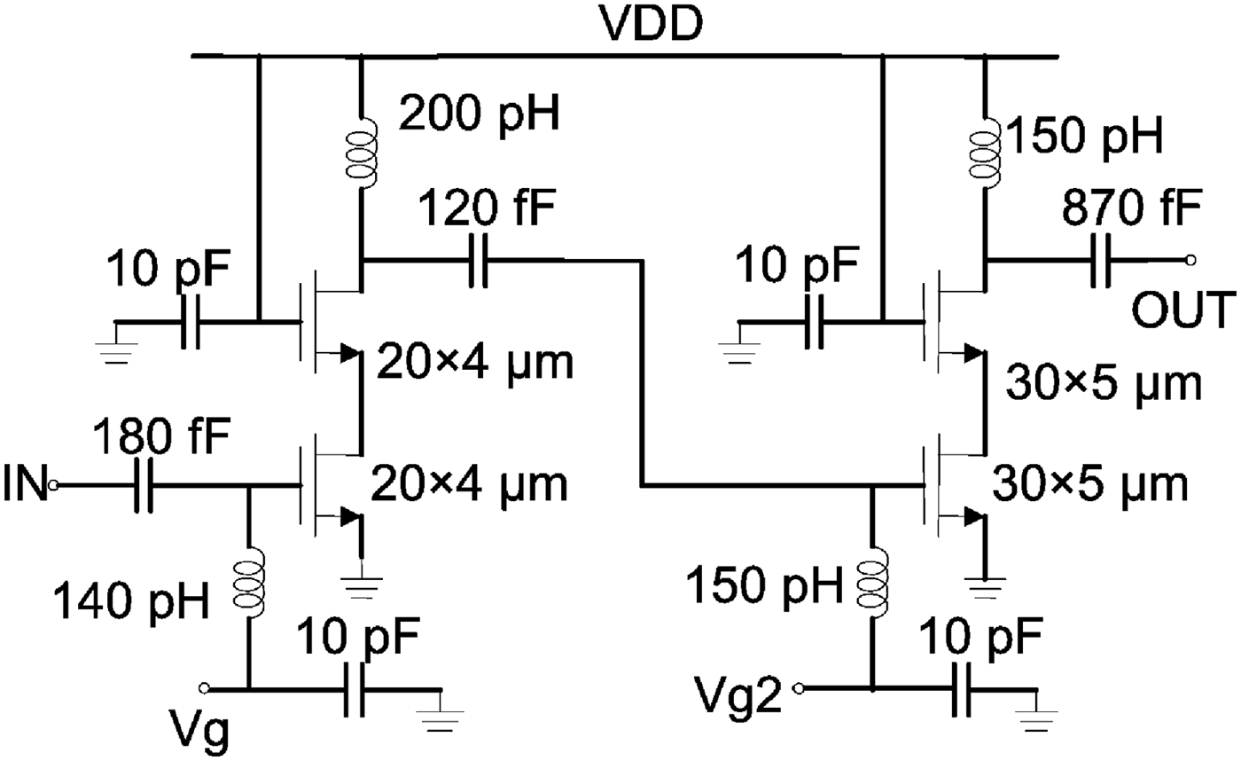
The transmitter is composed of two amplifier stages: a buffer stage and a power stage. Figure 3 shows the schematic of the transmitter. In the buffer stage, 20 × 4 µm transistors are used. The input matching is realized by a 180 fF capacitor and a 140 pH inductor. The inter-stage matching network between buffer stage and power stage includes a 120 fF capacitor and a 200 pH inductor. 10 pF blocking capacitors are used to decouple the RF and DC grounds.
Fig. 3. Transmitter schematic.
The implemented power stage is similar to the power amplifier output stage in [Reference Hamidian, Ebelt, Shmakov, Vossiek, Tao Zhang, Subramanian and Boeck19]. The transistor sizes of 30 × 5 µm have been selected for both common gate and common source transistors. The current flowing through the PA is 17.5 mA which is equal to 120 µA/μm current density. This current density has been derived from several optimization techniques for trade-off among PA efficiency, output power, and gain. Shunt inductors and series capacitors are used at output terminals to match the output to 50 Ω. Since the power amplifier signal leakage to the VCO could deteriorate the VCO PN, it is critical to reduce the leakage. Unlike [Reference Hamidian, Ebelt, Shmakov, Vossiek, Tao Zhang, Subramanian and Boeck19], triple well transistors are implemented in the transmitter to reduce the signal leakage into the substrate. The P-well of the triple well transistor and the ground of the stage are connected together as a separate ground. The power supply is also connected to a separate pad. With separated power supply and ground, the isolation between the transmitter and VCO can be ensured.
C) Receiver front-ends
The receiver front-ends are designed based on the receivers of [Reference Subramanian, Zhang and Boeck20], a variable gain amplifier (VGA) similar to the one in [Reference Hamidian, Ebelt, Shmakov, Vossiek, Tao Zhang, Subramanian and Boeck19] and an extra LO buffer is introduced to boost the performance. The LNA is a three-stage cascode LNA similar to that of [Reference Subramanian, Zhang and Boeck20]. It has 21 dB gain, 5 dB NF, and it consumes 13 mW from a 1.2 V voltage supply. The LO buffer amplifier is similar to the buffer stage of transmitter. However, the source impedance of the buffer amplifier differs as the transceiver changes between the SCR mode and the MCR mode. The input matching network of the LO buffer is modified accordingly to optimize the buffer gain at both modes.
The schematic of the mixer in the receiver front-end is shown in Fig. 4. It is a single balanced passive mixer with complementary switches similar with the mixer in [Reference Subramanian, Zhang and Boeck20]. Compared with [Reference Subramanian, Zhang and Boeck20], a biasing circuit is introduced to improve the mixer performance. For maximum conversion gain, the mixer transistors should be biased closely to the threshold voltage [Reference Saunders5]. Since the threshold voltage of the transistor is a function of process variations, biasing voltages and temperature, a compensating biasing circuit is designed in this work. Two low-threshold-transistors are diodes connected to provide the common mode voltage (VCM), the PMOS biasing (VP) and the NMOS biasing (VN). The diodes are biased slightly above the threshold voltage through a 10 µA current source (I b in Fig. 4). Since the low-threshold-transistor has a lower threshold voltage than the standard transistor, by adjusting the transistor size, the gate biasing voltages V N and V P can bias the mixer transistors slightly below the threshold voltage. The biasing current is trimmed to compensate the mismatch between the transistors.
Fig. 4. Schematic of the mixer.
IV. INTEGRATION CONSIDERATIONS
The chip micrograph of the four-channel transceiver is shown in Fig. 5. The four receivers, the transmitter, VCO, and divider are integrated into a small chip area of 2.2 mm × 1.7 mm.
Fig. 5. Transceiver chip micrograph.
50 Ω transmission lines are used for interconnections. Side-shielded microstrip [Reference Hamidian, Subramanian, Ran, Malignaggi and Boeck21] is chosen to minimize the leakage of the RF signal to substrate and to adjacent components. The transmission lines are set as short as possible to reduce the signal loss, while bends and T-junctions are avoided as they introduce high losses at 24 GHz. To suppress the coupling between different receiver channels, guard rings are placed on the edge of different circuit blocks. These guard rings include the metal lines and vias from the top metal to the bottom metal and to the substrate. The guard rings provide sufficient isolation between adjacent channels. The four Rx channels are also placed symmetrically to avoid performance mismatch.
V. SIMULATIONS AND MEASUREMENTS
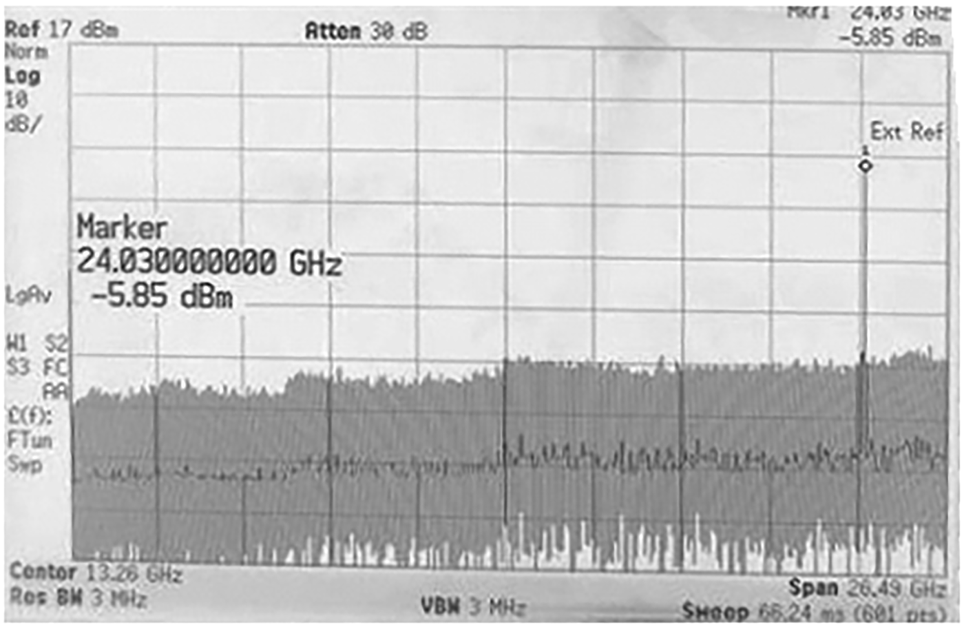
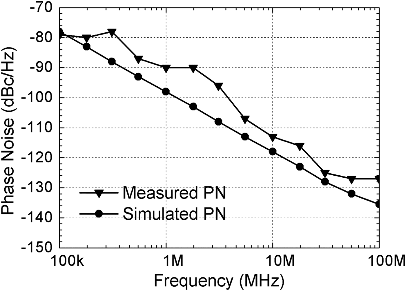
The integrated transceiver chip is on-wafer characterized and compared with the simulation results. The performance of the integrated VCO is characterized through a spectrum analyzer. Low-noise power supplies are used to measure the PN accurately. As depicted in Fig. 6, the measured VCO has an output power of −5.85 dBm with an operation frequency at 24.03 GHz. The tuning voltage is set at 0.4 V. Figure 7 shows the simulated and measured PN curve of the integrated VCO. The measured PN is −90 dBc/Hz at 1 MHz offset. It is 8 dB higher than that of the simulated PN, which is mainly due to the power supply PN and the inaccuracy of the device models at 24 GHz.
Fig. 6. VCO output spectrum.
Fig. 7. Measured and simulated VCO PN.
The individual TX and RX are then characterized. As external LO power can be sent to the circuit through the RF test pads at the RX/TX LO input, individual TX and RX can be measured separately with other circuits turned off. The transmitter is measured using a signal generator to generate the LO signal and a spectrum analyzer to measure the output signal. Figure 8 shows measured and simulated output power and power-added efficiency (PAE) of the transmitter versus the LO input power at 24 GHz. The maximum output power is 5.3 dBm and the maximum PAE is 10.4%. The measurement shows less output power and PAE than the simulation. This is mainly because the power supply and ground nets introduce extra parasitic degeneration to the cascode amplifier stages.
Fig. 8. TX output power and PAE versus LO input power.
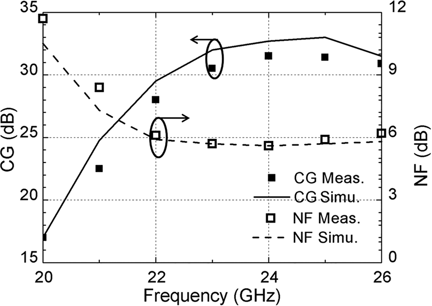
The RX is also characterized separately with an external LO signal applied to the test pad. The RF input is connected with a signal generator and the corresponding IF output port is connected with a spectrum analyzer. The gain and NF of the RX versus the LO frequency with −7 dBm LO power is shown in Fig. 9. The IF is 10 MHz. The RX has 31 dB gain and 5.6 dB NF at 24 GHz.
Fig. 9. RX conversion gain and NF versus LO frequency.
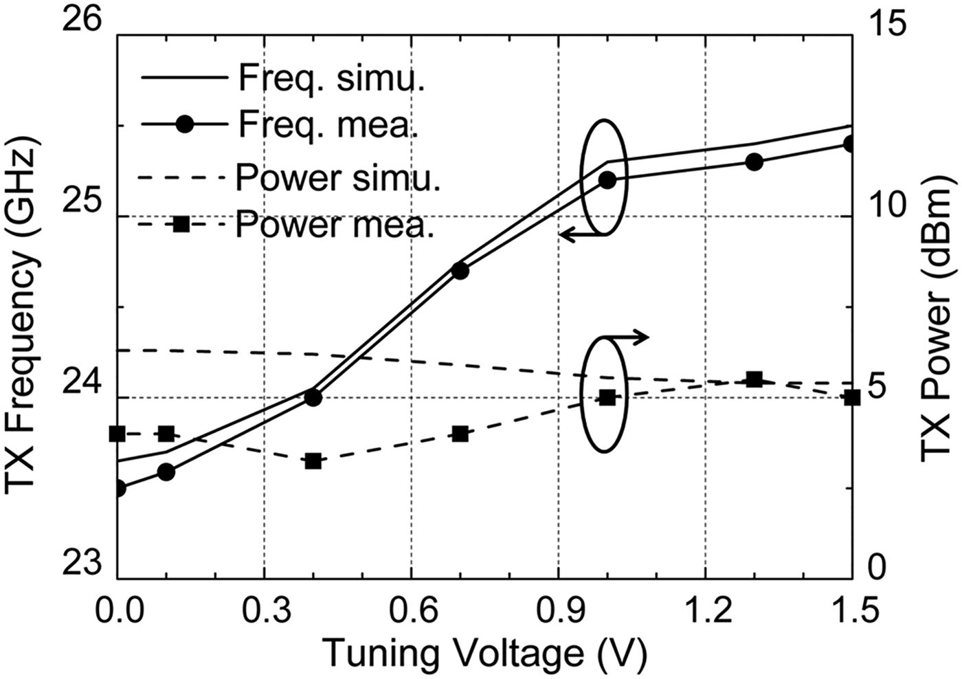
The integrated transceiver is on-wafer characterized in three different modes: transmitting, SCR, and MCR. In the transmitting mode, the transmitter and the LO generation circuits are turned on. The transmitter output signal is characterized by a spectrum analyzer connected to the TX output pad. The simulated and measured transmitter power and frequency is shown in Fig. 10. As the coarse tuning voltage changes from 0 to 1.5 V, the output power varies from 4 to 5.5 dBm, which is relatively constant. The frequency tuning range is from 23.5 to 25.4 GHz. If the tuning voltage is between 0.4 and 1 V, the Kvco is linear and the frequency ranges from 24 to 25.2 GHz can be covered. The percent linearity is less than 10% when the tuning voltage is between 0.4 and 1 V, which is suitable for FMCW radar applications. The power consumption is 75 mW with 1.5 V Vdd. The transmitter could efficiently cover the 24 GHz operation band.
Fig. 10. Output power and frequency versus tuning voltage in transmitting mode.
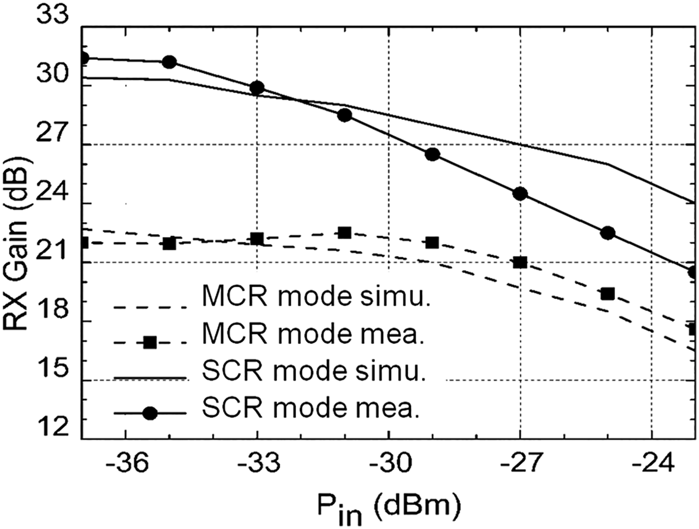
The receiving modes of the transceiver are characterized by a RF signal generator connected to an RF input and a spectrum analyzer connected to the corresponding IF output. Figure 11 shows the receiver gain versus RF power in MCR mode and SCR mode. The RF is 24 GHz and IF is at 5 MHz. In the SCR mode, the receiving channels are switched on and off one by one. The receiver achieves 31 dB gain, −33 dBm input P1 and 6 dB NF with 65 mW power consumption in the measurement. In MCR mode, the transmitter is turned off and all four receiver channels are turned on at the same time. The measurements show a gain of 21 dB, input P1 dB of −37 dBm and NF of 9 dB. The power consumption is 133 mW with 1.5 V biasing voltage.
Fig. 11. RX gain versus RF input power in MCR mode and SCR mode.
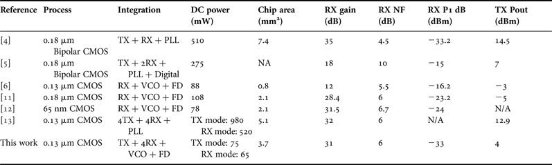
The transceiver performance is concluded in Table 1. The designed multi-mode transceiver front-end has achieved high performance, low-power consumption and high integration in comparison with the other state-of-the-art works.
Table 1. Performance comparison with other 24 GHz CMOS transceivers.
VI. CONCLUSION
A low-power switch-channel transceiver front-end, utilizing a power saving technique for wireless localization is designed, fabricated, and measured. The transceiver chip achieves high performance while keeps minimum chip area and power consumption. This design enables the wireless sensor networks with accurate wireless localization function.
ACKNOWLEDGEMENT
This work is part of the project LOWILO (BMBF Project No. 16SV3654). The authors wish to acknowledge BMBF for sponsoring and the project partners for their support.
Tao Zhang was born in Wuhu, China in 1983. He has received his Bachelor's degree in Applied Physics from the University of Science and Technology of China in 2004, and his Master's degree in Microelectronics and Solid-State Electronics from Chinese Academy of Sciences in 2007. He has worked toward his Ph.D. degree at Microwave Engineering Laboratory, the Technical University of Berlin from 2007 to 2011. Since 2012 he is working as IC design engineer at IMST GmbH, Germany. His research interests include RF and analog circuit blocks for millimeter and radio-frequency applications.
Amin Hamidian has been working since 2008 in the Microwave Engineering Laboratory, TU-Berlin where he received his Ph.D. degree with focus on the 60 GHz transceiver RF front-end design based on Si-CMOS and SiGe-HBT technologies. His main areas of research are in passive and active component modeling, PAs, transceiver front-ends and system design, packaging and board design techniques, and test and measurements for both microwave and mm-wave frequency bands.
Ran Shu was born in Nanjing, China. He received his M. Eng. degree in Electrical Engineering from Southeast University, China, in 2009 and Dr.-Ing. degree in Electrical Engineering from the Technische Universität Berlin (TU Berlin), Germany, in 2014. While with TU Berlin, he was involved in the design of K- and V-band CMOS RFICs. His main research interests are in the design of integrated microwave and millimeter-wave circuits based on CMOS technology.
Viswanathan Subramanian has been working since 2006 in the Microwave Engineering Lab, TU-Berlin where he received his Ph.D. degree in 2009 with the focus on enabling techniques for silicon-integrated transceiver circuits. His research interests include silicon-based radio-frequency and millimeter-wave integrated circuits.