I. INTRODUCTION
SU8 is an epoxy-based negative photoresist, which is often used for patterning or as sacrificial layers in MEMS processing. Recently SU8 has been used as device material also for RF-MEMS applications. WR-03 band rectangular waveguides fabricated by CNC milling, KMPR-based LIGA and with SU8 have been compared to each other by Shang et al [Reference Shang, Ke, Wang and Lancaster1]. They presented that the SU8-based rectangular waveguide insertion loss (~0.031 dB/mm for 220–325 GHz) have a comparable level with the commercially available CNC precision-machined metal waveguides (~0.02dB/mm for 220–325 GHz). These results show that SU8 could be a promising material to fabricate high-performance high-frequency waveguides.
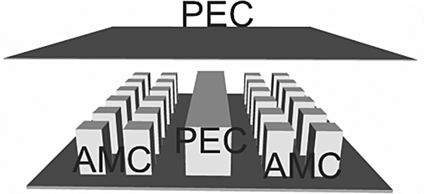
Gap waveguide technology is based on utilizing a metamaterial, in this case a bed of nails [Reference Silveirinha, Fernandes and Costa2], which forms an artificial magnetic conductor (AMC). When a perfect electrical conductor (PEC) is placed opposite an AMC, a parallel-plate stopband is created for a certain frequency band [Reference Rajo-Iglesias and Kildal3]. However, if the AMC layer incorporates a guiding structure such as a ridge, groove or strip, waves can propagate along the ridges, grooves or strips without leaking away from the structure [Reference Kildal, Alfonso, Valero-Nogueira and Rajo-Iglesias4]. Such parallel-plate structures can be used as transmission lines as shown in Fig. 1. The wave is prohibited to propagate outside the ridge due to the stopband as shown in Fig. 2.

Fig. 1. Illustration of a ridge-gap waveguide. The ridge and the lid are PEC surfaces and the pin-surface realizes the AMC surface.
Fig. 2. Two-dimensional color plot of the absolute value of E-field for the open circuit ridge-gap waveguide resonator.
A gap waveguide demonstrator for 10–20 GHz was presented in 2011 [Reference Kildal, Zaman, Rajo-Iglesias, Alfonso and Valero-Nogueira5] and since then different gap waveguide applications have been demonstrated below 50 GHz such as filters [Reference Zaman, Kildal and Kishk6] and packaging of MMICs [Reference Zaman, Alexanderson, Vukusic and Kildal7]. We have also demonstrated gap waveguides and their low loss at high frequency above 100 GHz, such as the ridge-gap waveguide resonator made in Si for 220–325 GHz [Reference Rahiminejad8], the pin-flange adapter [Reference Rahiminejad, Pucci, Haasl and Enoksson9, Reference Rahiminejad, Pucci, Haasl and Enoksson10], and the groove-gap waveguide for 100 GHz [Reference Rahiminejad, Raza, Zaman, Haasl, Enoksson and Kildal11, Reference Rahiminejad12]. The resonator is used as a demonstrator of the low losses of gap waveguides through measurements of the Q-factor of the resonance. The SU8 material is advantageous for manufacturing gap waveguides because of its relative low cost and simple process that lends itself well for mass production and provides high flexibility in 3D fabrication.
In this paper, we present the first polymer-based gap waveguide component, a ridge-gap waveguide resonator for 220–325 GHz made out of a two-layer Au-coated SU8.
II. BACKGROUND
The design is based on the ridge-gap resonator for 220–325 GHz presented in [Reference Rahiminejad8]. It consists of a ridge surrounded by pin structures, Fig. 3. The ridge is surrounded by two rows of pins along the long sides of the ridge and one row of pins on the connecting side (the short side). The coupling to the resonator needs to be weak, which is why there is one pin-row at the connecting sides. The pins and the ridge both have the same height of 277 µm±10 µm. The surrounding pins each have a top area of 165 µm×165 µm. The gap between the pin-surface and the PEC lid needs to be smaller than λ/4 for the stopband to exist. Here it has been chosen to be 167 µm from the design curves presented in [Reference Rajo-Iglesias and Kildal3] to get a stopband between 210 and 340 GHz.
Fig. 3. Top view of the ridge-gap resonator, displaying the dimensions and placements of the pin and the ridge.
The lid is part of a support package also presented in [Reference Rahiminejad8]. Figure 4 shows the support package with space for the ridge-gap resonator and a gap of 167 µm realized in the top part of this space. The package is used to support the chip when the measurement flanges are connected to it. The setup can be seen in Fig. 5, where (a) is a network analyzer (Agilent N5250C) connected to (b) a millimeter-wave controller (Agilent N5260A). The millimeter-wave controller is coupled to two OML extenders constructed for 220–325 GHz (c) where WR03 flanges (d) are connected to each side of the resonators support package (e), Fig. 4.
Fig. 4. A picture of the support package used during measurements with the PEC lid incorporated above and a schematic view of the opening which can fit the ridge-gap resonator and have gap of 167 µm above it.
Fig. 5. Measurement setup with a photo of the resonator being measured. (a) The network analyzer (Agilent N5250C), (b) the millimeter-wave controller (Agilent N5260A), (c) OML extender, (d) WR03 flange, and (e) support package for the resonator (Fig. 4).
The previous ridge-gap resonator was completely made out of silicon and coated with gold. The full process involved several process steps such as sputtering, lithography, ICP DRIE, stripping, gold sputtering, gold electroplating, and dicing. Measurements were done on the silicon ridge-gap resonator and compared to simulations with the same dimensions. The measurements of the previous silicon resonator can be seen in Fig. 6, [Reference Rahiminejad8].
Fig. 6. Measurement and simulation of the previous Si ridge-gap resonator [8].
The difference with the new ridge-gap resonator presented here in this paper is that instead of making it out of silicon, it is made of a two-layer SU8, coated with gold. The first layer acts as a carrier and the second layer determines the pin and ridge height. The pin width is 165 µm and its intended height is 277 µm.
III. FABRICATION
The fabrication process presented in this paper has been optimized for the ridge-gap resonator structure. SU8 2150 from micro resist technology was dispensed on a 4″ Si carrier wafer. First, it was spun at a low speed of 500 rpm to distribute the SU8 over the surface, and then it was spun at 2300 rpm to reach the desired thickness of the carrier layer, Fig. 7(b). It was then soft baked in two steps, first at 65°C for 10 min followed by a bake at 95°C for 55 min on a hotplate, Fig. 7(c). The two soft-bake steps are to avoid that the surface develops a crust that prevents the solvent to evaporate, and to reduce stress.
Fig. 7. (a) Si wafer, (b) first layer of SU8 dispensed, (c) soft-bake, (d) flood exposure, (e) second layer of SU8, (f) second soft-bake, (g) patterning, (h) developing the SU8, (i) KOH etch of the Si, and (j) sputtering and electroplating of Au.
It is quite common that craters or bubbles appear after the soft-bake, which was not visible before the soft-bake, Fig. 8. This can be traced back to how the SU8 was dispensed on the wafer. Several dispensing techniques are discussed at the forum memscyclopedia [Reference Chollet13], to avoid this problem. In this work, the syringe technique, the squeegee technique, pre-heating the wafer, and the star-pattern have been tested. In the end a combination of pouring the SU8 directly out of the bottle and allowing it to relax for about 10 min between every process step, reduces stress and the appearance of craters and bubbles.
Fig. 8. Craters and bubbles appearing after the first soft-bake step, due to unsuccessful dispensing of the SU8.
The whole wafer was flood exposed for 62 s to supply enough energy for the SU8 polymers to crosslink, Fig. 7(d). According to MicroChems data sheet the SU8 2150 needs about 370 mJ/cm2 for crosslinking at these thicknesses. The exposure energy from the Suss MicroTec mask aligner was 6 mW/cm2.
A second layer of SU8 2150 was dispensed (Fig. 7(e)) and distributed at 500 rpm, and then spun at 2000 rpm to achieve the pin height of 275 µm. The wafer went through a second soft bake at 65°C for 10 min followed by a bake at 95°C for 120 min (Fig. 7(f)) and was finally patterned with a negative photomask in proximity mode, Fig. 7(g). Another post-exposure bake at 65°C for 5 min and at 95°C for 28 min was performed.
Finally, the whole wafer was developed with strong agitation for 20 min, Fig. 7(h). The strong agitation is needed due to that the pins will have strings of SU8 connecting them to each other otherwise. After developing for 20 min, the wafer was dipped in a new developer bath and then rinsed with Isopropanol. If white marks appear during drying after the IPA rinse, the wafer needs to be developed further.
After patterning, the Si was removed from the SU8 by immersion in KOH at 80°C . Left was a wafer completely made out of SU8, see Figs 7(i) and 9. The SU8 wafer was then diced with a Loadpoint Microace 3+ into resonators and sputtered with a seed layer of Ti/Au (50/200 nm). The SU8 resonator chip was finally electroplated with Au, Fig. 7(j). To avoid skin effects a rule of thumb is that the overall thickness of the metal coating should be larger than five times the skin depth. The skin depth at 280 GHz is 0.15 µm. Therefore, the Au-coating was decided to be 1 µm thick, the same as that was previously successfully used for this device fabricated in Si [Reference Rahiminejad8].
Fig. 9. A complete SU8 wafer.
The SU8 “wafer” is as easy to handle as a Si wafer of the same size. The SU8 wafer was diced, sputtered, and electroplated in the same way as the Si wafer in [Reference Rahiminejad8].
IV. RESULTS AND DISCUSSION
A) Fabrication results
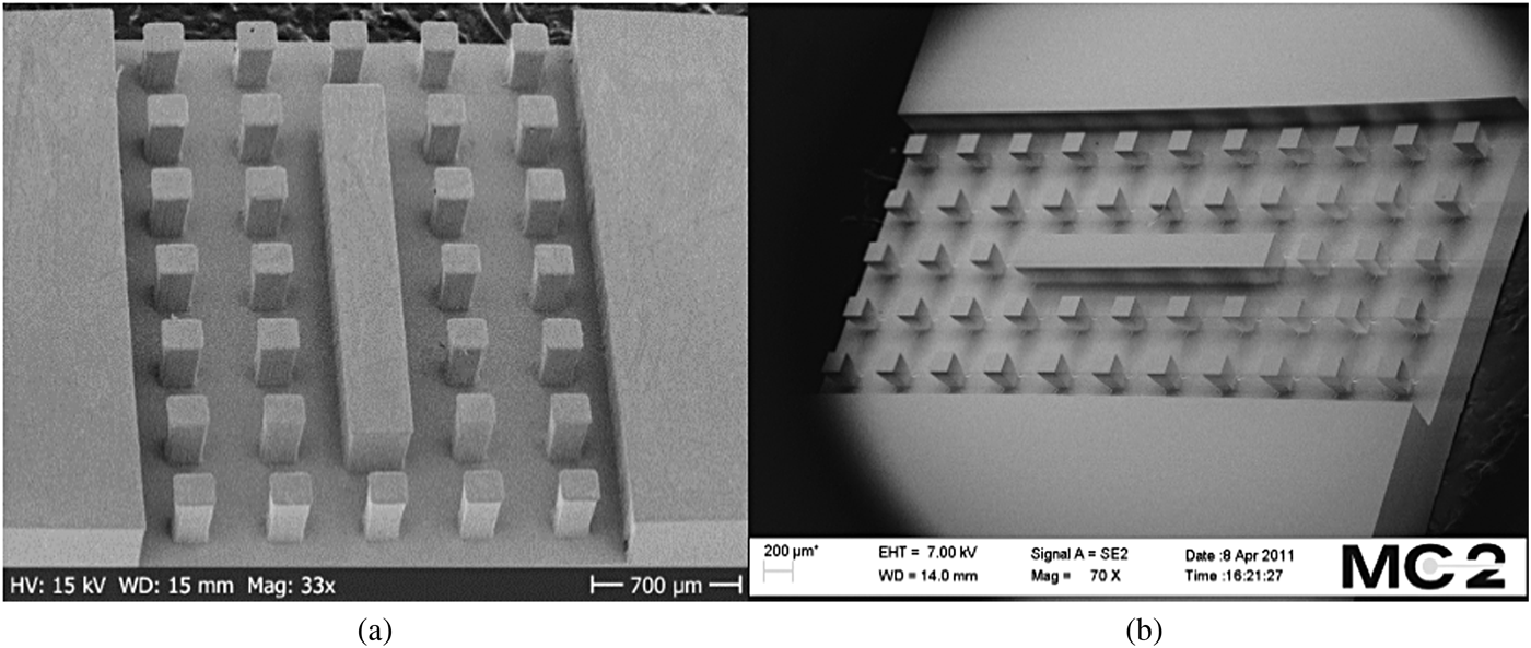
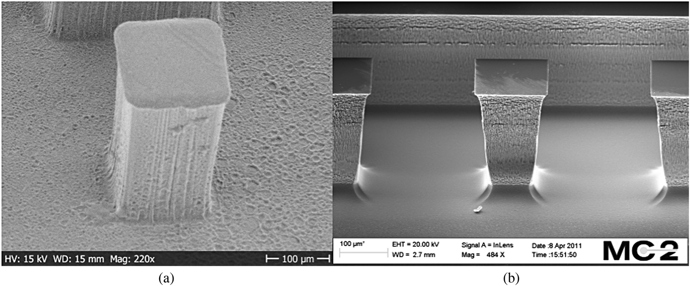
A two-layer SU8 ridge-gap resonator was fabricated. A SEM image of the SU8 resonator and the previous Si resonator can be seen in Fig. 10. The height of the pins is 275 µm, which is within 1% of the desired height of 277 µm. The top part of the pins is slightly wider which may broaden the bandwidth because it is closer to a mushroom shape that may have larger bandwidth [Reference Rahiminejad8, Reference Pucci, Rajo-Iglesias and Kildal14]. Figure 11(a) shows a SEM image of the SU8 pin and Fig. 11(b) shows a SEM image of the silicon pin. The silicon pin walls have a higher slope than the SU8 walls. The slope of the Si pin could probably result in a wider bandwidth than the SU8 pin; however, both structures will have a bandwidth sufficient for the WR-03 frequency band.
Fig. 10. SEM image of the (a) SU8 ridge-gap resonator, with a pin height of 275 µm and (b) Si-based ridge-gap resonator with a pin height of 275 µm.
Fig. 11. (a) SEM image of a SU8 pin on the SU8 carrier. (b) SEM image of the Si pins.
Fig. 12 shows the ridge-gap resonator made out of SU8 (Fig. 12(a)) next to the ridge-gap resonator made out of Si (Fig. 12(b)). Using SU8 as only structural material allows for future low-cost fabrication processes that entirely avoid the use of Si.
Fig. 12. (a) Ridge-gap resonator made out of only SU8. (b) Ridge-gap resonator made out of silicon.
The process time has been analyzed and is about the same as the Si-based process in [Reference Rahiminejad8]. The equipment used in the SU8-based process is cheaper compared to the Si-based process, where instead of using the STS ICP dry etching machine for a majority of the process time, a hotplate is used for a relatively long curing time. The material cost for the SU8 process is also lower than for the Si process.
B) Measured results
The measurements of the SU8-based resonator and the Si-based resonator were done for two frequency ranges, 220–260 GHz and 270–310 GHz. These ranges were selected such as to obtain a high number of measurement points around the resonance peak. The measurements of the SU8-based ridge-gap resonator and the Si-based ridge-gap resonator were compared to each other and to simulations, in Figs 13 and 14.
Fig. 13. Comparison between the measurements of simulations, Si and SU8 resonator at 220–260 GHz.
Fig. 14. Comparison between the measurements of simulations, Si and SU8 resonator at 270–310 GHz.
The resonance frequencies, the unloaded Q-values and the corresponding attenuation can be seen in Table 1. The attenuation was calculated from the unloaded Q-values with equation (1), [Reference Pucci, Zaman, Rajo-Iglesias, Kildal and Kishk15].
 $$\alpha=\beta /(2Q_u ).$$
Table 1. Measured unloaded Q-values and loss/mm.
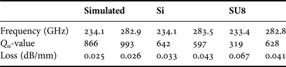
The resonance peaks for the SU8-based resonator match those of the Si-based resonator and simulations. The SU8-based resonator shows higher Q-values than the Si-based resonator at higher frequencies. The loss at higher frequencies is comparable to the Si-based resonator.
V. CONCLUSION
The first polymer gap waveguide resonator has been presented. The process of creating a two-layer SU8 device with SU8 both as carrier layer and as device layer has been successful. The SU8-based resonator has peaks close to the simulation and the previously presented fabricated Si-based resonator. The unloaded Q-values for the SU8-based resonator are higher for higher frequencies and an attenuation loss of 0.041 dB/mm at 282.2 GHz compared to the Si-based resonator with an attenuation loss of 0.043 dB/mm at 283.5 GHz. The SU8 process has fewer steps compared to the silicon-based process. SU8 is a more flexible material and therefore more robust, with a more cost-effective process.
ACKNOWLEDGEMENTS
This work has been supported by The Swedish Research Council VR, a project within the VINNOVA-funded Chase antenna systems VINN excellence center at Chalmers, and Chalmers production area of advanced science for funding of the reported work. The authors are grateful to the nanofabrication laboratory at Chalmers University of Technology for their help with the fabrication process.
Sofia Rahiminejad received her B.Sc. in Engineering Physics in 2009 from Chalmers University of Technology after that, she interned at Cornell University as a research assistant. She received her M.Sc. double diploma from both Katholieke Universiteit Leuven and Chalmers University of Technology in Nanoscience and Nanotechnology in 2011 as a part of the Erasmus Mundus master program. She has won two best poster awards at MME in 2012 and 2013. She is currently working toward her Ph.D. in the Micro and Nanosystems group at Chalmers University of Technology, Gothenburg, Sweden. Her interests lie in the field of micro- and nanosystems.
Elena Pucci received her M.Sc. degree in Telecommunication Engineering from University of Siena, Italy, in 2008, and the Ph.D. degree from Chalmers University of Technology, Sweden, in 2013. Her main research activity includes the development of the new gap waveguide technology for millimeter wave applications, with focus on losses study, packaging capabilities, and integration with antennas. Her background covers also the analysis of artificial magnetic conductors and electromagnetic band-gap materials, design of passive microwave components, small antennas, and arrays. She received the Second Best Student Paper Award at the European Conference on Antennas and Propagation (EuCAP 2012) in 2012 and the Best Poster Award at Micromechanics and Microsystems Europe Workshop in 2012. She joined Ericsson AB, Sweden, in 2014.
Sjoerd Haasl received his M.Sc. degree with high honors in Electrotechnical and Mechanical engineering from the University of Leuven, Belgium and the Ph.D. degree in Microsystem technology from the Royal Institute of Technology, Stockholm, Sweden. He was a research scientist and business area manager for the inertial sensors business platform at the research institute Imego, Gothenburg, Sweden until 2010. Currently, he works at the Center for Technology in Medicine and Health, a center funded by the Royal Institute of Technology, the Karolinska Institute and the Stockholm City Council. His interests lie in the fields of innovation and microsystems.
Peter Enoksson received his Ph.D. in 1997 from the Royal Institute of Technology, Stockholm, Sweden. In 1997, he became assistant professor and in 2000 he was appointed associate professor at the Royal Institute of Technology, working as project leader in the Microsystem Technology group. He was appointed Professor of MOEMS in 2001 at Chalmers University of Technology, Gothenburg, Sweden. In 2002, he was appointed vice dean of School of Electrical Engineering and in 2003 head of the Solid State Electronics Laboratory. He heads the Micro- and Nanosystems group, department of Microtechnology and Nanoscience and has published more than 200 research journal and conference papers, and has ten granted patents.