Introduction
High gain antennas have many advantages such as reduction of transmission power and increase in efficiency, performances, and transmission range of antennas. There are many methods that are used to increase the gain of antennas, such as the use of an antenna array, superstrate, and frequency selective surfaces (FSS) [Reference Stutzman and Thiele1]. A magnetic ground plane using artificial magnetic conductors is placed with a 2 × 2 antenna array for gain and bandwidth enhancement [Reference Yang, Wang, Che and Wang2]. An array of L-probe is used to suppress the surface waves and design is fabricated using low-temperature cofired ceramic (LTCC) technology to improve radiation performance [Reference Wang, Guo and Sheng3]. A two-layer antenna array of 32 × 32 patch antenna is designed using a substrate-integrated parallel feeding technology for gain enhancement for W-band applications [Reference Cheng, Guo and Liu4]. From the above literature, we can conclude that antenna array results in the complex feeding network as the number of array elements increases. To obtain the solution of complex feeding problems, a new feeding network Fabry–Perot is designed in [Reference Boutayeb and Nedil5]. Another gain enhancement technique that is based on superstrate-substrate resonance was developed such as placing an FSS structure [Reference Vaid and Mittal6], substrate having holes with an appropriate radius to control the permittivity generating an in-phase electric field [Reference Kim, Ahn and Bang7], and a three-layer superstrate of a low refractive index made up of a number of unit cells of metamaterial placed at an optimum height [Reference Li, Szabó, Qing, Li and Chen8]. A very high gain can be achieved at the desired angle just by choosing the proper thickness of substrate and superstrate. Multiple layers of superstrate are chosen based on their permeability and relative permittivity. All rays that passed through these superstrates are in phase and results in gain enhancement, which gives a better transmission range. Partially reflecting surfaces are used to reduce the radar cross-section and enhancement of gain of patch antennas [Reference Razi, Rezaei and Valizade9]. Metallic patterns are placed on both sides of a dielectric slab which act as a Fabry–Perot cavity along with the ground of a patch antenna, which is used to absorb the incident waves on the top side. To enhance the gain of microstrip antennas (MSAs), conical horn hybrid technology was also developed which is the most effective for short-range communication with a gain enhancement of around 6 dBi [Reference Elboushi and Sebak10]. A high gain reconfigurable polarized magneto-electric dipole antenna where a magnetic dipole is formed using aperture between the patches and horizontal patches with strip results in a planar electric dipole [Reference Ge, Yang, Zhang, Li and Wong11]. Three types of Artificial Magnetic Conductors (AMCs) are placed around a metasurface which is used as a radiator to achieve high gain in circularly polarized (CP) antennas and radar cross section reduction is achieved by creating a 90° phase discrepancy between AMCs and metasurface [Reference Jia, Liu, Gong, Zhang and Liao12].
With the growing demands of wireless devices such as mobile phones, wireless routers, and Internet of Things (IOT) devices, the need for the development of MSAs is growing very rapidly since their invention in 1969. The features such as small size, inexpensive, lightweight, planner, and low power consumption of MSAs make them most suitable for small handheld devices [Reference Wong13]. With the requirement of a device, this can work for a number of applications over different frequencies without any tuning which leads to research in the field of broadband antennas. Broadband antennas can eliminate the need for different antennas for different applications. These antennas are the antennas that provide good impedance matching over a wide frequency range and requires very little or no tuning. A broadband antenna can be used for several practical applications that fall under its operating range. A lot of research has been carried out in the recent past to enhance the bandwidth of MSAs using some of the techniques such as creating resonant structures by cutting different shapes like U-shaped slots [Reference Xu, Li, Yang, Wei and Qi14], E-shaped slots [Reference Deshmukh, Desai, Kadam and Ray15], V-shaped slots [Reference Rafi and Shafai16], aligned pentagonal shaped slots [Reference Shinde and Shinde17], and by adding multiple patches [Reference Targonski, Waterhouse and Pozar18]. These methods are used to create a new resonance frequency near the patches and help enhancing the bandwidth of the antenna.
In this modern age, where we are using wireless devices for communication needs a signal, which when transmitted through space gets distorted by environmental factors such as obstacles, noise, and multipath interference. To avoid multipath distortion and Faraday effect, CP waves are used. In the recent past, several CP MSAs have been designed, which are either right-hand CP (RHCP) or left-hand CP (LHCP). To generate CP waves from a linear polarization, a slit and a stub is placed on the ground plane along with an asymmetrical feed that provides an orthogonal component to the design [Reference Wu, Ke, Jou and Wang19]. An axial ratio bandwidth of more than 7% was achieved by using a 2 × 2 single-fed CP corner truncated patch array [Reference Deng, Li, Zhang and Feng20]. Multiband circular polarization can be achieved in a three-layered antenna structure using corner truncation, embedding slits, and inclined slots [Reference Singh, Kanaujia, Dwari, Pandey and Kumar21]. Another method to generate CP waves is using a 4 × 4 substrate-integrated waveguide feed to a slot-coupled rotated strip with a metal topped via fence fabricated using LTCC technology [Reference Li, Chen, Qing, Zhang, Xu and Feng22]. Reconfigurable polarization can be generated in an aperture-coupled structure by using two switches in a frequency band of 5.07–5.95 GHz for 5G Wi-Fi applications (5.15–5.725 GHz) [Reference Mak, Lai, Luk and Chan23]. A novel method is used to achieve quadband circular polarization in a MSA using two truncated patches with inclined slots and horizontal slits [Reference Singh, Kanaujia, Dwari, Pandey and Kumar24]. RHCP can be achieved using a square ring patch with two truncated diagonal corners excited with a single coaxial feed [Reference Hao, Lu, Chen and An25]. In [Reference Ullah and Koziel26], a wide band CP is achieved by inserting an L-shaped parasitic strip and slot modification. A quad-polarization reconfigurable antenna array is designed using four linearly polarized antenna elements which has two diagonal ports fed by grounded coplanar waveguide lines [Reference Hu, Hao and Hong27].
In this paper, we have presented a broadband high gain CP MSA using a metallic reflector surface. A metal sheet is positioned at an optimum height below the radiating patch which reflects the waves such that the resultant waves are in the same phase. Due to suppressed back lobe and in-phase reflected waves, a high radiation in the main lobe is achieved, and hence, increasing the gain of the proposed antenna. A split ring resonator (SRR) with rotating current [Reference Hao, Lu, Chen and An25] acts as a CP exciter for the metallic reflector, which makes the reflector as a secondary radiator and enhances the CP characteristics of the proposed design [Reference Nguyen, Tran and Nguyen-Trong28]. The proposed antenna shows a 10-dB impedance bandwidth of 71.64% in the frequency range of 4.30–9.10 GHz, a 3-dB axial ratio bandwidth of 33.88% from 4.98 to 7.01 GHz, and the maximum gain of 8.6 dBic.
Antenna design
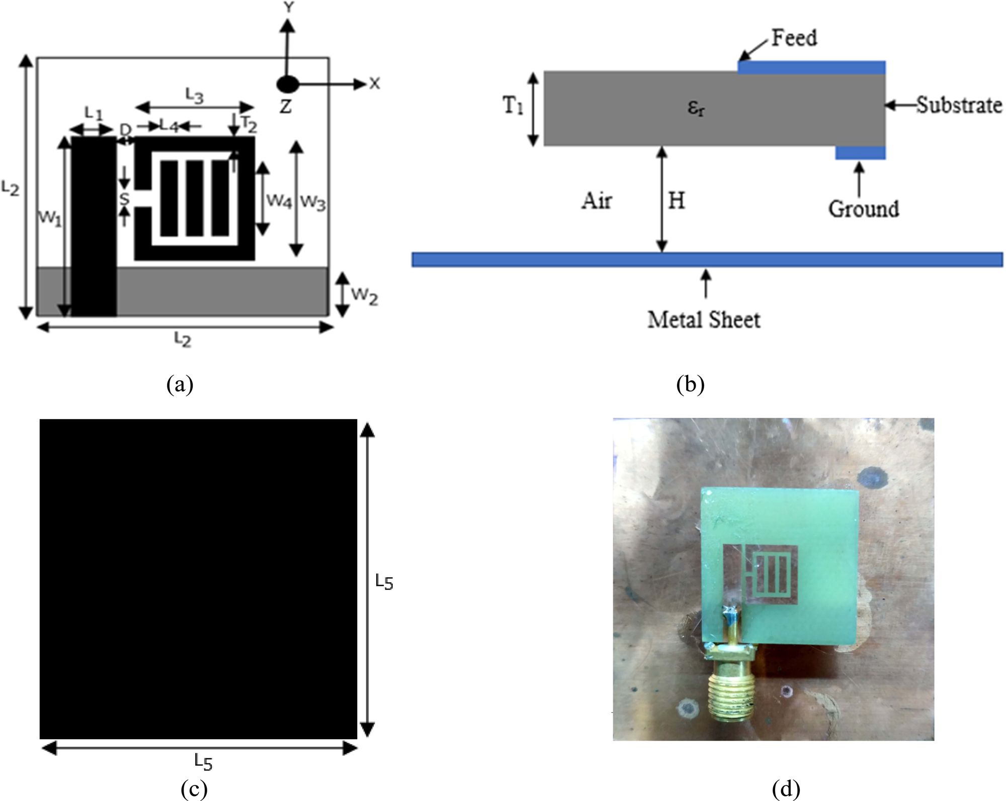
The proposed high gain CP MSA is designed on an FR4 square substrate with a length L 2 and thickness T 1 having a permittivity εr = 4.4 and a loss tangent (tan δ = 0.02). On one side of substrate, a monopole radiator with dimensions L 1 × W 1 is etched, which is entirely covered by ground with dimensions L 2 × W 2 on the other side of the substrate. A rectangular split ring of length L 3, width W 3, and thickness T 2, having a slot S is placed at a distance D away from the monopole radiator for wideband performance. Three rectangular metallic strips of length L 4 and width W 4 are placed inside the ring at an equal distance of 0.5 mm from each other and ring in order to increase in the gain little. The antenna is suspended at an optimum height H from a square reflector surface of length L 5. The two structures are suspended in such a way that the centers of both printed-circuit board and metallic reflector are aligned with each other (Fig. 1). The backward radiations are reflected with an angle of 180° by the metallic reflector that is added into the main radiation, resulting in the enhancement of the gain of antenna. The CP waves are generated by exciting a reflector by an SRR with rotating current in the proposed design. The anti-clockwise rotation of electric field vector results in RHCP waves for a frequency range of 4.98–7.01 GHz (Fig. 3). The proposed antenna structure is simulated and optimized using Ansys High-Frequency Structure Simulator (HFSS) Version 15. Table 1 shows the optimized dimensions of the proposed antenna. The antenna is fabricated using the data in Table 1 to validate the simulated results.

Fig. 1. The geometry of the proposed antenna: (a) proposed antenna, (b) front view, (c) metal reflector, and (d) fabricated antenna.
Table 1. Dimensions of the proposed antenna

Working principle of the proposed antenna
The proposed design shows the characteristics of wideband, high gain, and circular polarization. The wideband behavior is obtained due to the monopole patch radiator. By positioning the metallic reflector below the patch radiator enhances the gain and generates the circular polarization. This can be attributed to two factors. First, by placing the metallic reflector surface underneath the patch radiator results in the reflected waves in the same phase with main lobe radiation, thereby enhancing the gain. Second, the waves transmitted by a reflector are CP waves because the reflector is energized by a source which shows its characteristics approximate to CP. However, the detailed working principle of the presented antenna for both behaviors i.e. high gain and CP waves are discussed in detail in the following section. Due to monopole nature, the radiated wave from the upper plane gets divided into two parts E 1 and E 2 as shown in Fig. 2. Wave E 2 encounters 180° phase shift from reflecting surface and additional 180° phase shift due to path difference. Hence, total phase difference between direct radiating wave and reflected wave achieves 360°, which is the necessary requirement of the gain enhancement.

Fig. 2. Gain enhancement and generation of circular polarization using the metallic reflector in the proposed antenna.
Figure 2 shows that when a backward electromagnetic wave is incident on a metallic reflector, then the wave gets reflected back at an angle of 180° toward the main lobe in the same phase with main lobe radiation, resulting in gain enhancement of the proposed design. Total path difference may be calculated by evaluating effective dielectric constant [Reference Zhao29] of medium consisting of different dielectrics with different heights as
 $$\varepsilon _{reff} = \displaystyle{{H\varepsilon _{r_1} + T_1\varepsilon _{r_2}} \over {T_1 + H}}$$
where  $\varepsilon _{r_1} = 1\comma \;\;\varepsilon _{r_2} = 4.4$
 $$\lambda _g = \displaystyle{{\lambda _0} \over {\surd \varepsilon _{reff}}} = \displaystyle{C \over {\,f_d\surd \varepsilon _{reff}}}$$
where f d is the design frequency.
Here the path difference required is λ/2 with total height (H + T 1). Hence,
 $$H + T_ 1 = \displaystyle{{\lambda _g/2} \over 2} = \displaystyle{{\lambda _g} \over 4}$$
or
 $$\lambda _g = 4\lpar H + T_1\rpar $$
From equations (1)–(3), the air gap for a given design frequency can be calculated.
By placing an SRR on the right side of the monopole, the minimum value of axial ratio is around 4.5 dB at a center frequency of 5.9 GHz (Fig. 9). Again, by placing a metallic surface below the PCB at 0.2λ, this reflector enhances the CP performance of the antenna. As a result, the proposed antenna shows the wideband CP behavior. The wide band CP radiation of the proposed antenna is due to the combination of two CP radiators, including the SRR as an original CP exciter and metal surface as a secondary radiator [Reference Singh, Kanaujia, Dwari, Pandey and Kumar24]. In this design, we can say that the secondary radiator is utilized to generate a wide CP band, when excited by the CP exciter. The E-field rotates 90° in the anticlockwise direction in quarter time interval and hence generates the wideband CP. The direction of rotation of electric field with time decides the sense of polarization. In the presented design, the direction of rotation of electric field is in the anticlockwise direction that results in RHCP waves. Figures 3(a)–3(d) show the current distribution and the corresponding position of phase change point of current in the SRR at different time frames. As shown in Fig. 3(a), at t = 0, the phase change point of the current in the ring is at top of the left corner and shifted anticlockwise to the bottom of the left corner at t = T/4, as illustrated in Fig. 3(b). The position of the phase change point again rotates in anticlockwise and shifted to the bottom of the right corner of the ring at t = T/2, as depicted in Fig. 3(c). At t = 3T/4, the phase change point of the current reached the top of the right corner of the ring by rotating in the anticlockwise direction, as shown in Fig. 3(d).

Fig. 3. Rotation of phase change point of current in the SRR of the proposed antenna at 5.99 GHz.
From Figs 3(a)–3(d), we can observe that the position of the phase change point of the current in the SRR is rotating in the anticlockwise direction as the time elapses. Due to the rotation of current, electric field is also rotating in the same direction as phase change point of current does, as shown in Fig. 4.

Fig. 4. Effective electric moment in the anticlockwise direction at different time instants.
Simulation and measured results
HFSS software is based on the finite element method and is used for the design and simulation of the proposed antenna. The evaluation of the antenna is described in four different stages to demonstrate the various aspects of the proposed antenna design along with reflection coefficients in each stage and is shown Fig. 5. As shown in Fig. 5, initial design includes a printed monopole antenna with a modified ground plane (antenna A). Antenna A shows the wideband operation with the impedance bandwidth of 60.80% in the frequency range of 4.35–8.15 GHz. After that a slotted rectangular split ring i.e. an SRR is etched on the right side of the monopole radiator to increase upper resonance without disturbing the matching; as a result, there is increase in the impedance bandwidth as shown in Fig. 5 (antenna B). Three strips are inserted inside the rectangular ring (antenna C). A small effect on gain is observed at lower frequencies, but the gain increases as the frequency is increased with slight reduction in the impedance bandwidth on inserting the three strips inside the ring. This reduction in bandwidth is compromised on account of the gain increment. When we inserted the first strip inside the SRR and optimized its distance S from left edge of ring, there is an increase in the gain of 0.4 dBi for a frequency band around 8 GHz. We further inserted another strip inside the ring and optimized the distance from the first strip, and found that insertion of the second strip again improves the gain by 0.5 dBi in the same band, when placed exactly at the same distance S from the first strip. On inserting the third strip at equidistance S from the second strip, it further increases gain by 0.2 dBi in the band above 8.5 GHz and provides symmetry to the design. With the increase in the number of strips inside the ring results in increase in the effective area of the patch and improves the gain of structure. The maximum gain achieved in this design is 5 dB at 8.7 GHz. In order to increase the gain and to improve axial ratio further, in the final stage, a square metallic reflector is placed underneath antenna C and the height of reflecting surface is optimized to obtain the maximum gain along with CP operation. Finally, the structure of the proposed antenna (antenna D) is obtained as shown in Fig. 5. The comparison of reflection coefficients, gains, radiation patterns, and axial ratios of a proposed antenna with and without the metallic reflector is discussed in the following section. The simulated reflection coefficients for all the patch antenna designs are illustrated in Fig. 5. The center frequency of antenna C is 6.8 GHz with a bandwidth of 67.64% from 4.5 to 9.1 GHz. When the reflector is attached below antenna C, the center frequency decreases slightly to 6.7 GHz and a slight increase in the bandwidth is observed. The proposed antenna (antenna D) operates in the frequency band of 4.3–9.1 GHz with an impedance bandwidth of 71.64%. Figure 5 also shows the measured value of reflection coefficient for the proposed antenna. It has been observed that the values of reflection coefficient are approximately the same for simulation as well as the measured values. The little mismatch is due to the fabrication and material loss.

Fig. 5. Evaluation of the proposed antenna in different stages and its reflection coefficient.
A simple square metallic surface placed at an optimum height underneath the radiating patch is used to enhance the gain of the proposed antenna. The metallic reflector reflects all the back-lobe radiation in the boresight direction with an effective phase change of 180°. A comparison between the gains at the different stages of evaluation of the proposed design with and without the metallic reflecting surface as a function of operating frequency is shown in Fig. 6. From the figure, it can be seen that the gain of antennas A and B is approximately the same and the maximum gain obtained is 4.3 dBi, where antenna B shows larger bandwidth as compared to antenna A. It can also be seen from Fig. 6 that the gain is increased by about 1 dBi by inserting the strips in the ring (antenna C).

Fig. 6. Evaluation of the proposed antenna in different stages and its gain.
When the reflector is placed below antenna C (antenna D), the gain is almost stable and increased by 4.3 dBi. As shown in Fig. 6, the maximum gain achieved by the metallic reflector in the simulation of the proposed design is 8.6 dBic at a center frequency of 6.7 GHz. From the above results, it has been observed that the gain enhancement is successfully achieved over the operating frequency range and a little mismatch is observed in the measured and simulated gain as plotted in Fig. 6. The differences in the measured and simulated gains are due to the measurement and fabrication error. For the gain measurement of the proposed antenna, a linearly polarized horn antenna is employed and rotated 90° to obtain two orthogonal polarizations. The gain (G) of horn antenna is already known over an isotropic antenna. Both transmitting (test antenna) and receiving antennas are aligned in the direction of maximum radiation intensity and recorded the received power (PT). Then, the test antenna is replaced by a horn antenna and received power (PR) is measured again. The linear gain of proposed antenna is calculated using the below equation:
 $$\lpar {G_T} \rpar _{{\rm dB}} = \lpar {G_R} \rpar _{{\rm dB}} + \displaystyle{{ 10\,{\rm log\ }P_T} \over {P_R}}$$
and the gain of CP antenna can be calculated as
 $$\lpar {G_T} \rpar _{{\rm dB}} = 10\,{\rm log\ }\lpar {G_{TV} + G_{TH}} \rpar $$
where GTV is the partial power gain with respect to vertical linear polarization and GTH is the partial power gain with respect to horizontal linear polarization.
In order to study the radiation performance, the radiation pattern of radiating patch antenna without a metallic surface (antenna C) is shown in Fig. 7, while Fig. 8 shows the simulated and measured radiation patterns of the proposed antenna at a center frequency of 6.7 GHz. It is also noticeable that the front and back radiations are almost same. If back radiations are reflected at 90° out of phase CP may be obtained. From Fig. 7, we can see that the radiation pattern for a patch antenna without a reflecting surface, which have a large beam width and large back lobes as compared to the radiation pattern of proposed antenna at both ϕ = 0° and ϕ = 90° as shown in Fig. 8. Hence, positioning of the metallic reflector below the radiating patch reflects the backward waves in the same phase with main lobe radiation, thereby increment in the gain is observed. Figure 8 shows that the proposed antenna has a better front to back ratio.

Fig. 7. Radiation pattern of antenna without reflecting surface (antenna C) at a center frequency of 6.7 GHz.

Fig. 8. Radiation pattern of the proposed antenna (antenna D) at a center frequency of 6.7 GHz.
Figure 9 shows the variation of axial ratio with frequency at bore sight for the proposed antenna. From the figure, it can be seen that antenna without a reflector (antenna C) is linearly polarized, while the antenna with a reflector shows that the axial ratio at bore sight lies below the desired value for CP (AR ≤ 3-dB) in the frequency range 4.98–7.01 GHz with the center frequency of 5.99 GHz. The broadband CP radiation is obtained with a 3-dB axial ratio bandwidth of 33.88%. Figure 9 also shows the measured result of the axial ratio. The measured result of axial ratio agrees well with the simulated result. Figure 10 is a plot of simulated and measured RHCP and LHCP radiations at the center frequency of the CP band, which shows the RHCP is dominating the LHCP with a difference of more than 3-dB. Hence, the proposed antenna excites the RHCP wave. Simulated LHCP and RHCP are in consistence with the experimental results of the same.

Fig. 9. Simulated and measured axial ratio with and without the reflector.

Fig. 10. Simulated and measured radiation pattern of LHCP and RHCP of the proposed antenna at 5.99 GHz.
A detailed comparison between high gain CP antennas as of today is given in Table 2. From this table, we can conclude that the proposed high gain CP antenna exhibits broadband performance, good ARBW for RHCP with a high gain.
Table 2. Performance comparison with previously reported high gain CP antennas

Conclusion
A method to enhance the gain and generation of wideband CP radiation is proposed. The reflector reflects the backward radiation at 180° with an additional 180° phase difference due to path difference, resulting in the change in large in-phase radiation and hence improving the gain. The gain enhancement of 4.3 dBi is achieved. Wideband CP is achieved by exciting the metal reflector using SRR with a rotating electric field by 90° for every quarter time interval, which acts as a CP exciter for the metal reflector. The proposed suspended antenna shows an impedance bandwidth of 71.64%, a 3-dB axial ratio bandwidth of 33.88%, and a gain of 8.6 dBic. The proposed antenna exhibits the property of broadband impedance, wideband CP radiation, stable gain, simple to design, and easy to fabricate as compared to other high gain antennas. It is fed by a simple microstrip feeding resulting in no loss and a proper impedance match. The proposed antenna is fabricated and experimental results on reflection coefficient, gain, axial ratio, and radiation patterns conceded well with simulation results. The CP band covers a frequency range from 4.98 to 7.01 GHz and can be used in HIPERLAN/1 (5.1223–5.1729 GHz), Fixed Satellite Services (earth to space) (5.091–5.15 GHz), HIPERLAN/2 (5.471–5.71 GHz), and Amateur Satellite Uplink (5.65–5.67 GHz). The proposed antenna can also be used for 5G Wi-Fi (5.15–5.72 GHz).
 Arun Kumar received his B.Tech. degree in electronics and communication engineering from Gautam Buddh Technical University, Uttar Pradesh, India and his M.Tech. degree in electronics and communication engineering from the Amity University, Noida, India, in 2010 and 2013, respectively. He is currently pursuing his Ph.D. degree in microwave engineering with IIT (ISM), Dhanbad, India. His current research interest includes gain enhancement of microstrip antennas.
 Santanu Dwari received his B.Tech. and M.Tech. degrees in radio physics and electronics from the University of Calcutta, West Bengal, India, in 2000 and 2002, respectively, and his Ph.D. degree from the IIT Kharagpur, Kharagpur, India, in 2009. He is currently working in the Department of Electronics Engineering, IIT (ISM), Dhanbad, India, as an Associate Professor. He has published more than 100 research articles in refereed international journals/conferences. His current research interest includes computational electromagnetics, antennas, and RF planar circuits. He is carrying out two sponsored research projects as a Principal Investigator.
 Ganga Prasad Pandey received his B.Tech. in electronics engineering from K. N. I. T., Sultanpur, India in 2000. He completed his M.E. in computer technology and application at the Delhi College of Engineering, Delhi, India in 2004 and obtained his Ph.D. degree from Uttarakhand Technical University, Dehradun, India in 2015. Presently, he is an Assistant Professor in Information and Communication Technology department of Pandit Deendayal Petroleum University, Gandhinagar, India. His research interests include active, reconfigurable, frequency agile microstrip antennas and microwave/millimeter wave integrated circuits and devices.
 Binod Kumar Kanaujia received his B.Tech. degree in electronics engineering from the Kamla Nehru Institute of Technology, Sultanpur, India, in 1994, and his M.Tech. and Ph.D. degrees from the Department of Electronics Engineering, IIT (BHU), Varanasi, India, in 1998 and 2004, respectively. He is currently a Professor with the School of Computational and Integrative Sciences, Jawaharlal Nehru University, New Delhi, India. He has been credited to publish more than 250 research articles with more than 1600 citations and an H-index of 18 in several peer-reviewed journals and conferences. He had supervised 50 M.Tech. and 15 Ph.D. scholars in the field of RF and microwave engineering. He had successfully executed five research projects sponsored by several agencies of the Government of India, e.g. DRDO, DST, AICTE, and ISRO.
 Dinesh Kumar Singh received his B.E. in electronics and communication engineering from Kumaon University, Nainital, in 2003. He received his M.Tech. in digital communication from RGPV University, Bhopal, India and his Ph.D. from ISM, Dhanbad, India, in 2016. Presently, he is working as an associate professor in Electronics and Communication Engineering department of G.L. Bajaj Institute of Technology & Management, Greater Noida, India. His area of interest is microwave engineering.