


Introduction
Microwave is an electromagnetic radiation with an operating frequency ranging from 500 MHz to 300 GHz. A cross-field magnetron operates a household microwave oven as the microwave generator component. Heat is generated when the electric field intersects with the magnetic field at a prescribed angle. Food is heated by microwave through frequency absorption, and the container is not heated due to the difference in the absorption rate of the microwave frequency. The efficiency of the microwave system invented by Brown remains the best to date [Reference Brown1]; such a system achieves 92% efficiency in converting RF to DC and 55% efficiency in an RF 1 kW initial power transmission. Brown later managed to achieve 83% efficiency for 34 kW transmission over a mile for a high-power system. The number of reported research studies on microwave power transmission has backtracked slightly due to regulatory restriction for such high-power microwave exposure and limitation [Reference Brown1–Reference Brown and Eves5].
There are few general approaches reported in achieving high efficiency and low-power microwave generation in recent research studies involving semiconductors in microwave generators; for example, a ultra-wideband microwave generator using a low-energy-triggered bulk with the implementation of a gallium arsenide (GaAs) avalanche semiconductor switchable to achieve a ultrafast switching period as low as ~200 ps [Reference Hu, Su, Qiu and Fang6]. The silicon (Si) photonic integrated solution into an optoelectronic oscillator (OEO) for frequency-tenable microwave generation is also reported. The OEO developed from Si performs better with a high-resistivity metallic micro-heater and is thermally tunable [Reference Zhang and Yao7]. The solid-state device approach oscillates at a low-power microwave output of 210 W, 2450 MHz with an efficiency of 51%. It is reported that the solid-state injection-locked oscillator has a longer life and operates at lower voltage, with tunable phase and frequency [Reference Ikeda and Itoh8]. Thus, researchers assume that electron drift velocity control is essential to achieve high efficiency and reliable microwave power generation using a magnetron. This is explained by the unbalanced magnetic field control which affects instantaneous power consumed in the plasma, leading to sudden temperature rise. There are also other influencing parameters in the spatial distribution of a high-power impulse magnetron plasma sputtering process through a controlled unbalanced magnetic field [Reference Konishi, Takaki and Yukimura9].
Plasma sputtering on magnetron's cathode surface using gallium nitride (GaN) and silicon carbide (SiC) semiconductors is a technique used to enable high efficiency in the magnetron operation at high frequency in a low-power microwave generation. The conventional magnetron potentially generates 6 kW, 2450 MHz microwave power over 67% efficiency. However, if the same conventional magnetron with a non-sputtered cathode was used to generate 5 W, 2450 MHz low microwave power, the efficiency drops significantly to approximately 50%, as shown in the experiment. Losses occur during the generation process and hence lower the efficiency of the microwave power generation system.
A 6 kW, 2450 MHz rated continuous wave (CW) sintering thawing type magnetron with a model number CK-625 is used in this experiment. The magnetron is attached with a metal-ceramic and a water-cooling system with the integrated RF filter with industrial microwave heating applications. This model of magnetron is known for its rapid-heating cathode, high efficiency, and the required output power. The magnetron's cathode is made from oxide material, barium oxide (BaO), whereas GaN and SiC are categorized as semiconductors. The technique used in this study is to grow a 100 nm thick plasma layer of GaN and SiC on the magnetron cathode surface in a dedicated experiment. Further analysis and comparison during low-power microwave generation were executed. Other defining parts of the magnetron remain constant.
The preparation of the magnetron for low-power microwave generation involves direct sputtering to the magnetron's cathode surface. Uniformity in semiconductor deposition on the magnetron cathode surface is achieved through a specific sputtering process which differs by the deposition temperature and the material's period with respect to its characteristics. An improper sputtering process potentially leads to the leakage of electron flow to the internal layer of magnetron's cathode. It causes stability issues in the microwave power generation due to temperature spikes. Such a situation potentially leads to risks, such as an explosion due to unstable thermodynamic stability between the magnetron's cathode and semiconductor plasma coating applied. In this case, it is essential to have a high-quality sputtering process on the surface with high-quality semiconductor purity deposition growth.
Magnetron operating system
A magnetron is categorized as a diode because it has no grid. The anode of a magnetron is fabricated into a cylindrical concrete copper block, as shown in Fig. 1. The filament and cathode are located in the middle of the structure and lifted by the filament leads. The filament lead is rigid and large enough to hold the filament, with the cathode structure hooked in its position. The cathode is composed of a high-emission material and heated indirectly. The 8–20 cylindrical holes around its circumference are known as resonant cavities, which control the output frequency. A narrow slot runs from each of the cavity into the central portion of the tube, dividing the inner structure into many segments. The open space between the cathode and the plate is known as the interaction space. In this space, the magnetic and electric fields interact to exert force upon the electrons. The magnetic field is provided by a strong permanent magnet mounted around the magnetron so that the magnetic field is in parallel to the cathode axis.
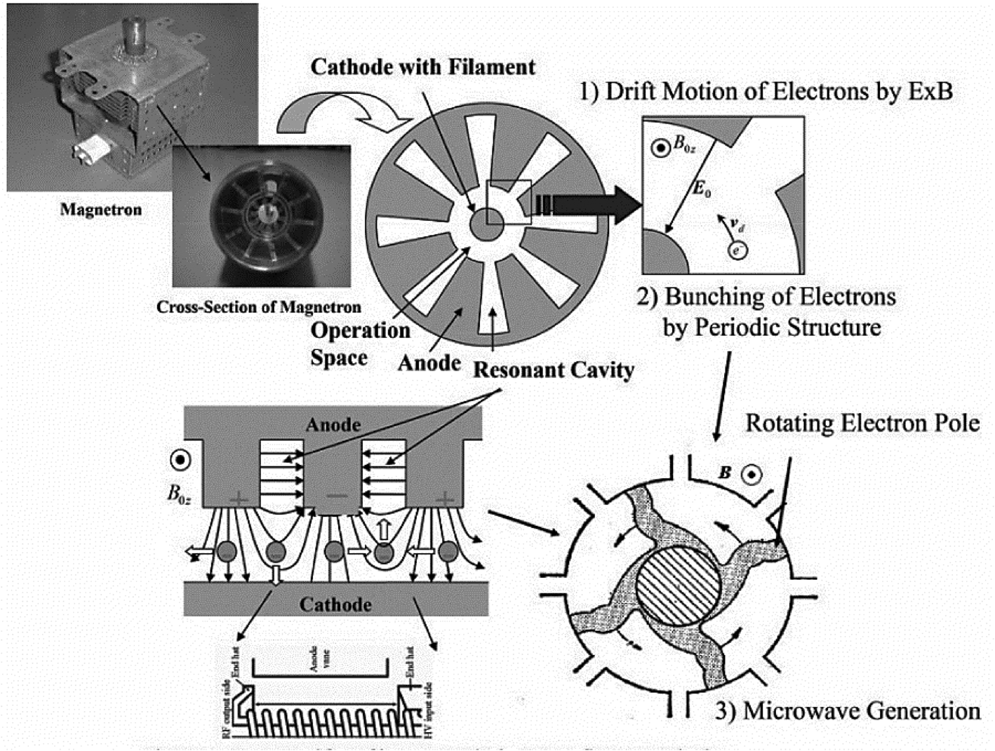
Fig. 1. Magnetron cross-section and parts.
Electron drift velocity relation
This experimental sputtering system is a modification from the sputtering process used to fabricate integrated circuit, ingot, and wafer growth. However, in this experiment the sputtering system is intended to grow an even plasma layer using SiC and GaN on the magnetron's cathode surface of a cylindrical shape. Therefore, the modification of a conventional sputtering system is necessary, which includes the deposition chamber enlargement to fit the magnetron's cathode during deposition with an additional transfer arm used to regulate the magnetron's cathode as a target, and with embedded additional safety features. The modification is necessary as the magnetron's cathode, which serves, as deposition target of size 80 mm, could not fit into the conventional sputtering system.
The objective of this sputtering is mainly to control the drift motion of electrons by E (electric field) × B (magnetic field) interaction space, as described in Fig. 1 between the cathode filament and anode. Drift motion is scientifically referred to as the drift velocity of a particle, such as an electron. During microwave power generation, electrons propagate freely on the magnetron's cathode surface at Fermi velocity. In this case, the average velocity of an electron is known as drift velocity, which results in a semiconductor due to the existing electric field [Reference Canali, Jacoboni, Nava, Ottaviani and Alberigi-Quaranta10–Reference Canali, Majni, Minder and Ottaviani12]. Scientifically, the drift velocity refers to the axial drift velocity. Therefore, with respect to the Fermi concept, the electron propagates freely in a semiconductor at the aforementioned Fermi velocity. When a small electric field is applied to a magnetron, the electron flows in random motion on the magnetron's cathode surface due to two main carrier mechanisms which are the ionized impurity scattering and lattice scattering. By referring to elementary Ohm's law, which states that current is proportional to the electron drift velocity subjected to material resistive, expressed as:

where u refers to the drift velocity; μ is the electron mobility (in m2/(V s)) of the semiconductor, in this experiment (GaN or SiC); and E is the electric field, in this study referred to as the microwave power generated. However, the sputtering of this semiconductor covers a sizeable cross-sectional area on the magnetron's cathode surface in which the dimension of the magnetron's cathode needs to be considered, of 80 mm length and 25 mm diameter. Therefore, the drift velocity of the charge in a magnetron's cathode surface with a constant cross-sectional is given as follows:

In this extended drift velocity equation, j represents the current density flowing through the magnetron's cathode, n is the number of charge-carrier density, and q is the charge associated with the change in carrier. By considering the properties of cylindrical current-carrying metallic ohmic semiconductor, with the charge-carrier of electron, the drift velocity is expressed as:

where m represents the semiconductor molecular mass in kg, σ is the electric conductivity in s/m, Δv is the voltage applied in V, ρ is the conductor density in kg/m3, e is the elementary charge in C, f is the free electron number, and l is the conductor length in m. The drift velocity, u is elevated by substituting the properties and parameters for each material, of GaN, SiC, and BaO (represent conventional magnetron), with Ga for GaN-sputtered magnetron, and Si for SiC-sputtered magnetron. However, the drift velocity computation in equation (2) not applicable for an oxide base, which includes BaO magnetron's cathode as it is not accounted as semiconductor material. This prohibition was strengthened by electricity commonly conducted in a copper wire. Magnetron's cathode, which is made from an oxide-based material, has a density of 8.94 g/cm3 and an atomic weight of 63.546 g/mol with a total of 140 685.5 mol/m3. Therefore, in an 80 mm thickness, the magnetron's cathode has about 6.8 × 1027 atoms ((6.02 × 1023 × 140 685.5 mol/m3) × 0.08 m). The reason being that copper-based magnetron's cathode has one free electron per atom, n is equal to 6.8 × 1027. By substituting the parameter in the drift velocity equation for BaO:

In addition, by considering the cross-sectional shape of the magnetron's cathode, the equation is further derived to be:

The electron for BaO in the magnetron's cathode is flowing at the rate of 23 μm/s with a constant AC supply of 60 Hz. This concludes that the electron drift is less than 0.2 μm below the half cycle. By considering the cross-sectional area full parameter in (5), including the operating temperature in electron, the Fermi flow velocity is computed as 1570 km/s for BaO with 721 and 987 km/s for GaN and SiC, respectively.
Sputtering process
From the analysis shown earlier, the sputtering process is expected to enable the magnetron to produce a low-power microwave with improved efficiency compared to the conventional magnetron by controlling the electron drift motion or known as electron movement speed. A lower electron motion speed generates lower heat density; this is the key in achieving a highly efficient magnetron. Therefore, in this process, the magnetron's cathode surface is deposited with two different types of semiconductors in dedicated experiments. Before the sputtering process begins, the magnetron's cathode is dismantled from the magnetron fixture and is grown with high purity GaN and SiC semiconductors. Figure 2 shows the magnetron's vertical cross section view with the cathode located in the mid-section of the magnetron. The dimension of the magnetron's cathode to sputter is 80 and 25 mm in diameter.
Fig. 2. Conventional magnetron cut-off.
The semiconductor selection with a higher melting point ensures the magnetron is safe to generate microwave power and is stable [Reference Chapin13, Reference Somekh14]. A strong coupling between the anode, cathode, and resonant cavity occurs during microwave power generation, as shown in Fig. 1. This strong coupling produces heat which commonly exceeds the temperature of 300°C. Therefore, materials used in a magnetron must hold a high degree of temperatures and have a high melting point to ensure its safety.
The semiconductors GaN and SiC are sputtered separately. Magnetron's cathode is made of the combination of high purity copper and oxide material, specifically, BaO, which has a superior conductance and able to generate high power microwave. Both semiconductors sputtered under different conditions of temperature and decomposition period in line with their respective characteristics, such as melting point temperature, material growth, and evaporation rate. Figure 3 shows the experimental setup for the magnetron cathode sputtering which is modified from a standard sputtering setup in semiconductor fabrication for integrated circuit development. Generally, there are three main types of sputtering: confocal sputtering, in-situ tilt sources in a confocal sputtering system, and direct sputtering. The sputtering process used in this experiment is direct sputtering as it only involves one material at the same time.

Fig. 3. Sputtering process equipment setup: (a) front view and (b) side view.
Therefore, as the magnetron's cathode diameter is sputtered at 80 mm, a direct sputtering method is chosen due to its suitability to the chamber design. Direct sputtering is able to achieve ±10% of decomposition uniformity on the magnetron's cathode surface.
The magnetron's cathode cylinder is fixed into the deposition chamber cage in a horizontal position and attached to the transfer arm. A voltage of 2 kV is supplied to the cathode throughout the process to produce a strong magnetic field around the cathode cylinder for semiconductor seed deposition. A manual control panel is used to control the rate and pressure of flammable gas pumped into the deposition chamber while controls the movement of the semiconductor plate and transfer arm when the chamber is ready to be ramped toward the desired deposition temperature. An integrated power supply is used to power up all valves and motors used in this operation. A high-temperature monitoring camera is attached to the deposition chamber's top position and connected to a computer for the observation of deposition (Fig. 4).

Fig. 4. Deposition chamber.
With the chamber pre-heated up to 950°C and subsequently achieving the desired deposition temperature, the transfer arm is used to shift the magnetron's cathode into the mid-section of the chamber. The cathode being the deposition target requires to be pre-heated simultaneously; a 2 kV voltage is supplied to the cathode to ionize the seed from the substrate holder at the bottom. Due to ionization, the seeds are pulled and semiconductor grows at a constant rate; hence the deposition period is initiated. The cathode keeps rotating at a constant rate and is pushed into the chamber using a transfer arm to deposit the semiconductor onto the other parts of the cathode surface.
The sputtering process is repeated with different deposition parameters at 950, 1100, and 1250°C, with respective deposition periods of 7, 9, and 11 min for each semiconductor. The same variation of parameter was applied for both materials to examine its deposition result. Several sputtering periods at different deposition temperatures are adopted, and physical analysis was performed through the observation of morphology images.
The surface quality of the sputtered magnetron's cathode is chosen based on the physical evaluation of morphology images for a uniform semiconductor. It is observed that SiC is best to be sputtered at 950°C for 7 min while GaN is best at 1250°C for 5 min of sputtering. GaN sputtering is executed slightly above 1200°C, ensuring a perfect plasma deposition growth on the magnetron's cathode surface without leaving out any uncovered surface on the metal. The combination of Ga and nitride (N) has changed the material characteristic to produce GaN and SiC with 2500 and 2730°C melting points, respectively. Figure 5 shows an example of GaN morphology image taken at different deposition temperatures. GaN sputtered at 1250°C is bound to be more decisive than the BaO layer. The gray color background shows that GaN is bounded with BaO, with the images taken at 1100 and 950°C. A clear vision of boundary between GaN in white color and BaO in the black color is visible. The semiconductor is not entirely grown, and the same comparison is made for different deposition materials and periods.
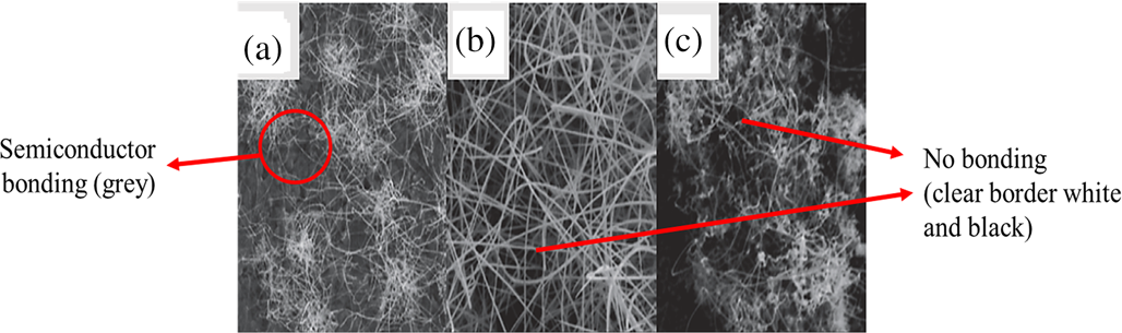
Fig. 5. GaN morphology images: (a) 1250°C, (b) 1100°C, and (c) 950°C.
Another parameter of consideration to ensure better semiconductor seed deposition is the thickness of the plasma layer grown. The thickness is regulated through a quartz crystal microbalance using a surface profilometer. Prior to placing the semiconductor seed, the surface profilometer, which is located under the seed plate, is calibrated to determine the thickness of seed deposition and to estimate the deposition rate. However, there is no specific calibration for temperature, and the deposition period differs in this experiment. As tabulated in Table 1, three different plasma thicknesses of 80, 100, and 120 nm are compared.
Table 1. Sputtered magnetron efficiency comparison

Experimental validation
After the magnetron cathode is sputtered with GaN and SiC, it is then re-assembled into the magnetron core in measuring its performance. The magnetron is used to generate 5 W microwave power using 2450 MHz for each test. The power supply of 5 V is used for the magnetron; however, in this case, the magnetron is placed in a closed anechoic box for health and safety purposes during the experiment. Therefore, a combination of transformer and capacitor is used to replace the power supply, as shown in Fig. 6. The magnetron, as shown in Fig. 6, illustrates the connection before it is placed in a chamber. The magnetron output terminal is connected directly in series to waveguides, coaxial matched load, and copper cavity flange to the measurement system components for further analysis.

Fig. 6. Experimental measurement setup diagram.
The purpose of using WR340 waveguide coupling is for magnetron frequency pulling measurement supported by the hall probe sensor so that the microwave power signal generated follows the drive current for measurement. Figure 7 shows the measurement setup after the magnetron is placed in a closed anechoic box and connected through waveguides. Measurement system components include the network analyzer measuring the scattering parameter with isolation at load, spectrum analyzer, power supply, and oscilloscope. The measuring system is divided into two parts: on the left side is the power transmitter, while the rectenna is on the right side.
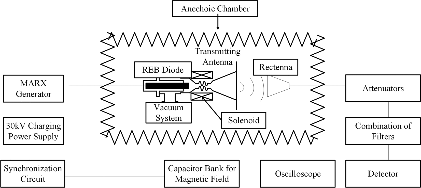
Fig. 7. Diagram of measuring system.
Figure 8 shows the magnetron's output current captured through a spectrum analyzer for SiC and GaN magnetron cathodes. However, the output current from the conventional magnetron is beyond the measurable limits due to unstable operation. The comparison between SiC and GaN magnetrons is observed. There is a noticeable current distortion for SiC and expected higher total harmonic distortion (THD), as recorded in Table 1. GaN produces less distortion and smooth output current, which is easily filtered to obtain an ideal waveform.

Fig. 8. Spectrum analysis of current waveform: (a) SiC and (b) GaN.
After determining the suitable deposition temperature and period for each semiconductor, the process is repeated with different thicknesses of deposition through the surface of profilometer located under the seed plate which is calibrated to determine the thickness of seed deposition and to estimate the deposition rate. The seed plate is adjusted manually for a higher density seed release rate after each deposition process ended, and the magnetron cathode width is measured and the test results for different thicknesses are summarized in Table 1.
After the magnetron is sputtered with GaN and SiC, the THD percentage improves, which results in an enhancement of microwave power generators performance through magnetron sputtering, contributing to the higher efficiency of transmission. The THD is recorded during the generation of 5 W with sputtered magnetron at frequency 2450 MHz for communication devices’ charging application. This application is not limited to mobile charging but also in powering wireless sensor network devices, Internet of Things devices, and medical wearable. All communication circuitry requires the compliance with strict guidelines on the THD limit produced on board. The sputtering process with different deposition thicknesses on the magnetron's cathode reacts in a THD reading consistent for both SiC and GaN materials compared to the conventional magnetron, where prior to sputtering, the THD remains high and unstable. THD, low harmonic distortion (LHD), and efficiency for conventional magnetron are recorded as 27.52, 12.3, and 37%, respectively (Table 2).
Table 2. THD recording

The magnetron efficiency using the conventional magnetron, specifically with BaO magnetron cathode to generate 5 W at 2450 MHz, triggers the cooling system through the thermo-switch attached to the magnetron. The magnetron thermo-switch snaps after an approximate operation of 10 s. Referring to the analysis earlier, the conventional magnetron efficiency in generating low-power microwave remains not more than 67% for CW type sintering thawing magnetron, similar to the efficiency achieved in [Reference Amankwah and Pickles15–Reference Meier and De Swardt18].
Analysis and comparison
This study reports the first ever experimental measurement results on surface plasma sputtering to the magnetron's cathode, measuring its efficiency enhancement. Therefore, a comparison was constructed in measuring the magnetron's performance before (conventional magnetron) and after sputtering highlighting the comparison between different sputtering materials of GaN and SiC. Figure 9 shows the efficiency of each magnetron. The conventional magnetron architecture has a power loss of almost 33% and incurs more losses with respect to time. Severe noise also occurs when utilizing the conventional magnetron to generate 5 W of microwave power. SiC-sputtered magnetron gives a stable output of microwave power but still observes a negligible noise due to the vibration of magnetron's cathode surface. In conclusion, SiC and GaN achieve highest efficiency with almost no noise.

Fig. 9. Power output comparison.
In appreciating the noise produced by the magnetron's cathode vibration during microwave power generation, Fig. 10 shows the noise comparison measured using a network analyzer. Magnetron's cathode sputtered with SiC produces slightly higher noise than with GaN.

Fig. 10. Noise comparison.
The main setback that affects the preference in SiC-sputtered magnetron's cathode is the efficiency, whereas the preference of GaN-sputtered magnetron's cathode is in the noise produced. The vibration measured using a vibration analyzer indicates that SiC produces higher vibration compared to GaN. Vibration observed with GaN is 3470.83 mm/s RMS equivalent to 45 Hz, while SiC produces 4110.19 mm/s vibration equivalent to 38 Hz. The vibration analysis is recorded during 5 W microwave power generation using a magnetron at a microwave frequency of 2450 MHz. The vibration is initiated due to the drift motion of the electron, as discussed earlier.
By using two different types of materials for the magnetron's cathode plasma, the sputtering process has achieved the objective of controlling the electron drift motion on the magnetron's cathode. Hence, analysis shows that GaN-sputtered magnetron's cathode have favorable characteristics for RF, microwave, and Terahertz devices compared to SiC-sputtered magnetron's cathode [Reference Binari, Klein and Kazior19–Reference Christou24]. Table 3 summarizes the relation of electron drift velocity calculated and the efficiency during the generation of microwave power at 5 W for each material.
Table 3. Magnetron's efficiency and electron drift velocity

The efficiency of the magnetron computed based on the fundamental efficiency equation is given as below:

From the analysis presented, if the electron drift velocity flow is reduced, the efficiency of the microwave power generated is higher due to low-power generation resistance. However, if the sputtered SiC or GaN solution is used for high microwave power generation, the efficiency drops due to unbalanced electron flow in the magnetron's cathode.
A comparative analysis is summarized in Table 4 [Reference Daimon and Jiang25–Reference Chek, Mekhilef, Sulaiman and Krishnamurthi33]. The proposed solution improves the efficiency significantly by 50% with the GaN and SiC plasma layers compared to the conventional counterpart. In principle, there exists a severe trade-off between the output power and the efficiency due to temperature rise. The trade-off exhibited by GaN- and SiC-coated magnetron cathode is in its unsuitability to generate high power after being sputtered. However, there is still no apparent solution in addressing the trade-off.
Table 4. Comparison with recent studies

Conclusion
The SiC and GaN plasma layers are fabricated on magnetron's cathode by an RF direct sputtering method. Semiconductor deposition on magnetron's cathode surface has proven to increase the efficiency of low microwave power generation by 50%. By conducting a full test on microwave power generation system, THD and generated power performance is enhanced compared to the conventional magnetron. GaN-sputtered magnetron's cathode performs better than SiC-sputtered magnetron's cathode in the efficiency exhibited and the incurred noise.
Acknowledgements
The authors would like to thank the Ministry of Higher Education, Malaysia under the Long Term Research Grant Scheme (LRGS): LRGS/1/2019/UKM/01/6/3 and the University of Malaya, Malaysia for providing financial support under the Faculty research grant: GPF056A-2020.
 Leong Wen Chek received his B.Eng. degree in electrical and electronics engineering from Universiti Malaysia Pahang in 2013, his Master of Engineering (Science) from the University of Malaya in 2016, and is currently pursuing his Ph.D. degree in power electronics and renewable energy. His main research interests are design and optimization of wireless power transmission using modulated microwaves. He was with Motorola Solutions (M) Sdn. Bhd in 2011 attached as a Product Engineer.
 Saad Mekhilef (Senior Member, IEEE) received his B.Eng. degree in electrical engineering from the University of Setif, Setif, Algeria in 1995, and his master's degree in engineering science, and his Ph.D. degree in electrical engineering from the University of Malaya, Kuala Lumpur, Malaysia, in 1998 and 2003, respectively. He is currently a Professor and the Director of the Power Electronics and Renewable Energy Research Laboratory, Department of Electrical Engineering, University of Malaya. He is also the Dean of the Faculty of Engineering, University of Malaya. He is also a Distinguished Adjunct Professor with the Faculty of Science, Engineering and Technology, School of Software and Electrical Engineering, Swinburne University of Technology, VIC, Australia. He has authored or co-authored more than 400 publications in international journals and conference proceedings. His current research interests include power converter topologies, control of power converters, renewable energy, and energy efficiency.
 Harikrishnan Ramiah is currently an Associate Professor at the Department of Electrical Engineering, University of Malaya, working in the area of analog ICs, RFIC, and RFEH design. He received his B.Eng. (Hons), M.Sc. and Ph.D. degrees in electrical and electronic engineering, in the field of analog and digital IC design from Universiti Sains Malaysia in 2000, 2003, and 2008, respectively. He is the Head of the Center of Industry Research 4.0 (CRI 4.0) and the Director of the Analog, Digital & RF research group at the University of Malaya. He was with Intel Technology, Sdn. Bhd in 2007 attached as a Senior Component Design Engineer. In 2003, he was with SiresLabs Sdn. Bhd, CyberJaya, Malaysia with a dedicated role as a Senior Design Engineer. Harikrishnan was the recipient of Intel Fellowship Grant Award, 2000–2008. He is a Chartered Engineer of Institute of Electrical Technology (IET) and also a Professional Engineer registered under the Board of Engineers, Malaysia.


