Introduction
With the advent of the modern multi-service system, it is necessary to provide a stable transceiver to establish the requirement of wireless communication condition. Of particular interest are dual-wideband (DWB) microwave devices. In recent years, many DWB bandpass filters (BPFs) have been presented [Reference Liang, Wang and Kim1–Reference Hsu, Chien and Tu12]. Open stub-loaded coupled-line sections [Reference Xu and Wu2] is introduced to develop DWB BPF while the selectivity between the two passbands is low. The cross-stub stepped impedance resonator in [Reference Firmansyah, Praptodinoyo, Wiryadinata, Suhendar, Wardoyo, Alimuddin, Chairunissa, Alaydrus and Wibisono3] has the advantage of compact size and wide bandwidth while isolation between the two passbands is low. The transversal signal-interaction concept [Reference Zhou, Feng and Che4] is introduced to develop DWB BPF. In [Reference Li, Huang and Zhao5–Reference Zhang and Zhu7], DWB BPF is achieved utilizing multi-mode resonators while suffering from the relative size. In [Reference Denis, Song and Hang9], it may be embarrassed for their narrow bandwidths, which is difficult to meet the requirement of high data rate, high transmission capacity, and multi-service in modern communication systems [Reference Xiong, Wang, Pang, Zhang, Zhang, He, Zhao and Zhang8]. In [Reference Zhang and Zhu10], mutually coupled SIRs are used as the basic filter block. In this design, the filter is proposed using open-shorted coupled lines (OSCL) Contrasted with other papers, the bandwidth can be adjusted in a wide range and low insertion, compactness, high selectivity and isolation can also be achieved
Structure and analysis
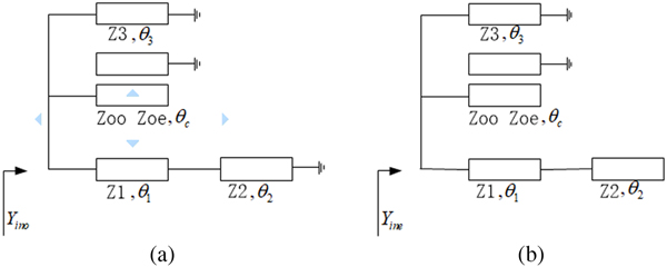
The topology of the proposed DWB bandpass filter is demonstrated in Fig. 1. It is fed by 50 Ω transmission line directly and consists of a pair of short-ended stubs and OSCL (Z oo, Zoe, θc) and a single-stepped impedance transmission line. Its equivalent transmission line model acquired through odd–even mode analysis method is shown in Figs 2(a) and 2(b). Zi(i = 1,2,3,c) and θ j(j = 1,2,3,c) indicate the microstrip characteristic impedance and electrical length, respectively.
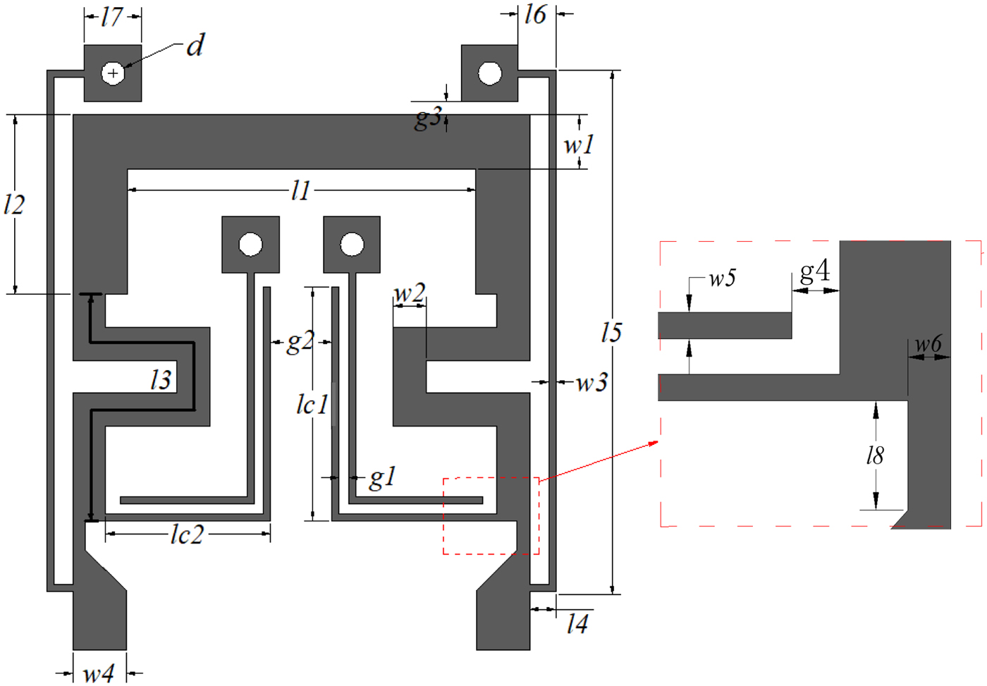
Fig. 1. Topology of the proposed filter.
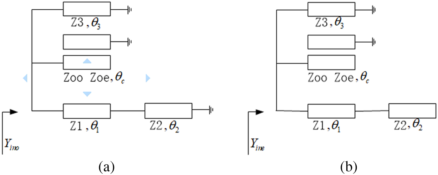
Fig. 2. Odd-mode (a) even-mode (b) equivalent circuits of the proposed filter.
The matrices of the coupled lines and stubs can be obtained from [Reference Matthaei, Young and Jones13] after ABCD-, Y-parameter conversions. Equations (1) and (2) demonstrate the input admittance when excited by odd and even modes, respectively.
 $$\eqalign{ Y_{ino} &= - j\displaystyle{{\lpar {Z_{oe} + Z_{oo}} \rpar \sin 2\theta _c} \over {{\lpar {Z_{oe} - Z_{oo}} \rpar }^2 - {\lpar {Z_{oe} + Z_{oo}} \rpar }^2cos^2\theta _c}} \cr & \quad - j\displaystyle{{Z_1 - Z_2tan\theta _1tan\theta _2} \over {Z_1\lpar {Z_2tan\theta_2 + Z_1tan\theta_1} \rpar }} - j\displaystyle{1 \over {Z_3tan\theta _3}},} $$
 $$\eqalign{ Y_{ine} & = - \,j\displaystyle{{\lpar {Z_{oe} + Z_{oo}} \rpar \sin 2\theta _c} \over {{\lpar {Z_{oe} - Z_{oo}} \rpar }^2 - {\lpar {Z_{oe} + Z_{oo}} \rpar }^2\hbox{co}\hbox{s}^2\theta _c}} \cr & \quad - j\displaystyle{{Z_1tan\theta _2 + Z_2tan\theta _1} \over {Z_1^2 tan\theta _1tan\theta _2 - Z_1Z_2}} - j\displaystyle{1 \over {Z_3tan\theta _3}}.} $$
The transmission poles (TP) and zeros (TZs) can be derived by making the input admittance equal to zero and tend to infinity, respectively. Then four solutions can be obtained and is shown in equations (3–6) considering the infinite case.
 $$\theta _3 = 0;$$
 $$\theta _3^{\prime} = \pi \, ;$$
 $$\theta _c = arccos\displaystyle{{Z_{oe} - Z_{oo}} \over {Z_{oe} + Z_{oo}}};$$
 $$\theta _c{\rm ^{\prime}} = {\rm \pi} - arccos\displaystyle{{Z_{oe} - Z_{oo}} \over {Z_{oe} + Z_{oo}}}.$$
To reasonably allocate the TZs, equation (4) which indicates the highest frequency of TZ should be placed right around the TZ equation (6) indicates for. So we get the relationship between θ 3 and θ cin equation (7)
 $$\theta _3 = {\rm \pi} \theta _c/\left( {{\rm \pi} - arccos\displaystyle{{Z_{oe} - Z_{oo}} \over {Z_{oe} + Z_{oo}}}} \right). $$
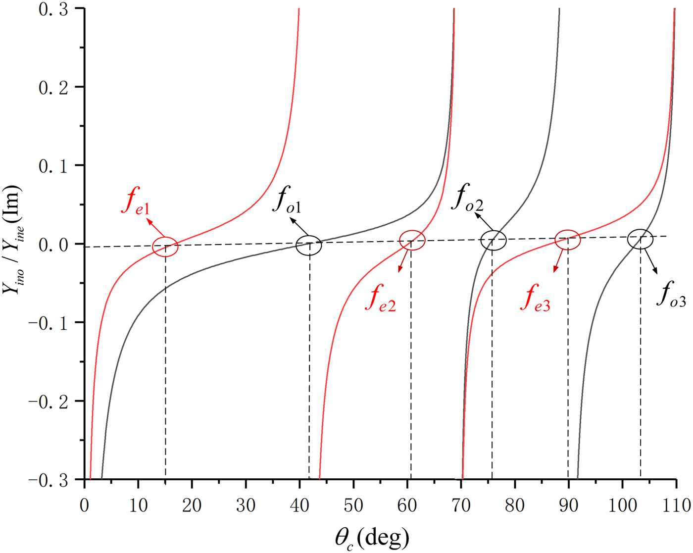
To simplify the calculation, we hypothesize θ 1 = θ 2 = θ c. By making the input admittance equal to zero, we can get the TP, which is under the condition Y ino = 0 or Y ine = 0 as depicted in Fig. 3. The first six TP can be divided into two parts, f e1, f o1, and f e2 form passband one, f o1, f e3, and f o3 form passband two.

Fig. 3. Analysis of TPs.
As for the TZ, there are five TZs as depicted in Fig. 4, owing to the λ/4 impedance transformation effect, the loaded uniform impedance short stub could bring virtual ground to the connection point, resulting in the achievement of TZ5 which has been expressed in equation (4). Similarly, after appropriate transformation on the ordinary short stubs, such as OSCL, we could obtain TZ1 and TZ4 which have been expressed in equations (5) and (6), respectively. So TZ1 and TZ4 are related with Z oe, Z oo which correspond to physical dimensions of g 1 and w 5.

Fig. 4. Analysis of TZs.
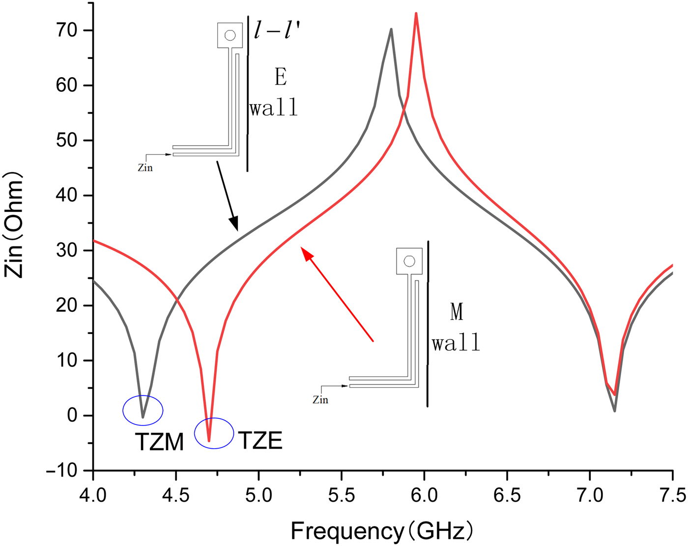
Except TZ1, TZ4, and TZ5, which have been analyzed above,TZ2 is formed due to the different input impedance of OSCL when the filter is considered as even mode excited or odd mode excited, thus leading to the split of TZ1. Figure 5 shows the differences when l-l′ is considered as electric wall and magnetic wall which corresponding to odd mode excited and even mode excited, respectively, we can get two different frequencies when making Zin (the input impedance of the OSCL section) equal to zero and thus causing the emerging of TZ2. In addition, TZ3 is achieved by source–load coupling, it can be controlled by changing g 2 and lc 1.

Fig. 5. Different input impedance of OSCL considering different boundary condition.
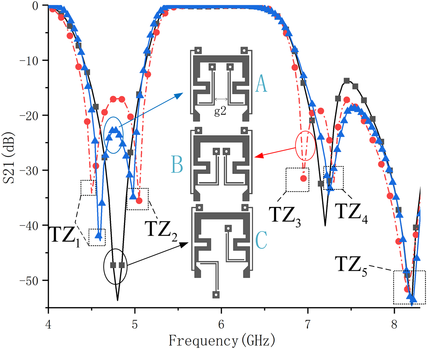
To verify the mechanism of TZ2 and TZ3 generation, three relevant structures are shown in Fig. 6 as A–C were simulated. TZs with different generation mechanisms are decomposed in the simulated transmission responses as shown in Fig. 6. It makes the comparison when the filter is with/without source–load coupling or the split of TZ1. In structure A, g 2 is greater than that in structure B causing the difference of TZ3. And in structure C, there is no couple between source and load, neither the distinction of even mode or odd mode excited. In addition, from equation (1–6), we can draw the conclusion that the TPs are determined by characteristic impedances of odd- and even-mode Z oo, Z oe as well as Z 1, Z 2 while the TZs are mainly determined by Z oo, Z oe. So on some level, the independent characteristics between TPs and TZs is good for the achievement of high selectivity. The TZs can be settled first by adjusting Z oo, Z oe, and then adjusting TPs by changing Z 1 and Z 2 aiming to close the space between the TZ and its neighboring TP.

Fig. 6. Transmission responses of relevant structures.
Relationships for the characteristic and some other parameters of the proposed filter are analyzed as below. It is known from the preceding paragraph, TZ1−4mainly depends on the OSCL sections, and the position of them determined central frequency and bandwidth. The central frequency and the bandwidth of the two passbands can be adjusted easily, as depicted in Fig. 7. From Fig. 7(a), making Z oo and Z oe changing toward a different trend has an impact on the width of both passband but in the opposite way, it can be achieved by changing g 1. From Fig. 7(b), with changing Z oo and Z oe toward the same trend, the FBW of the second passband can be adjusted from 8% (Z oo = 57Ω, Z oe = 101 Ω) to 30% (Z oo = 85 Ω, Z oe = 170Ω) while the central frequency of the second passband and the central frequency, as well as bandwidth of the first passband maintain still, it can be achieved by changing w 5, so the width of the two passbands can be adjusted independently through appropriate setting of Z oo and Z oe.
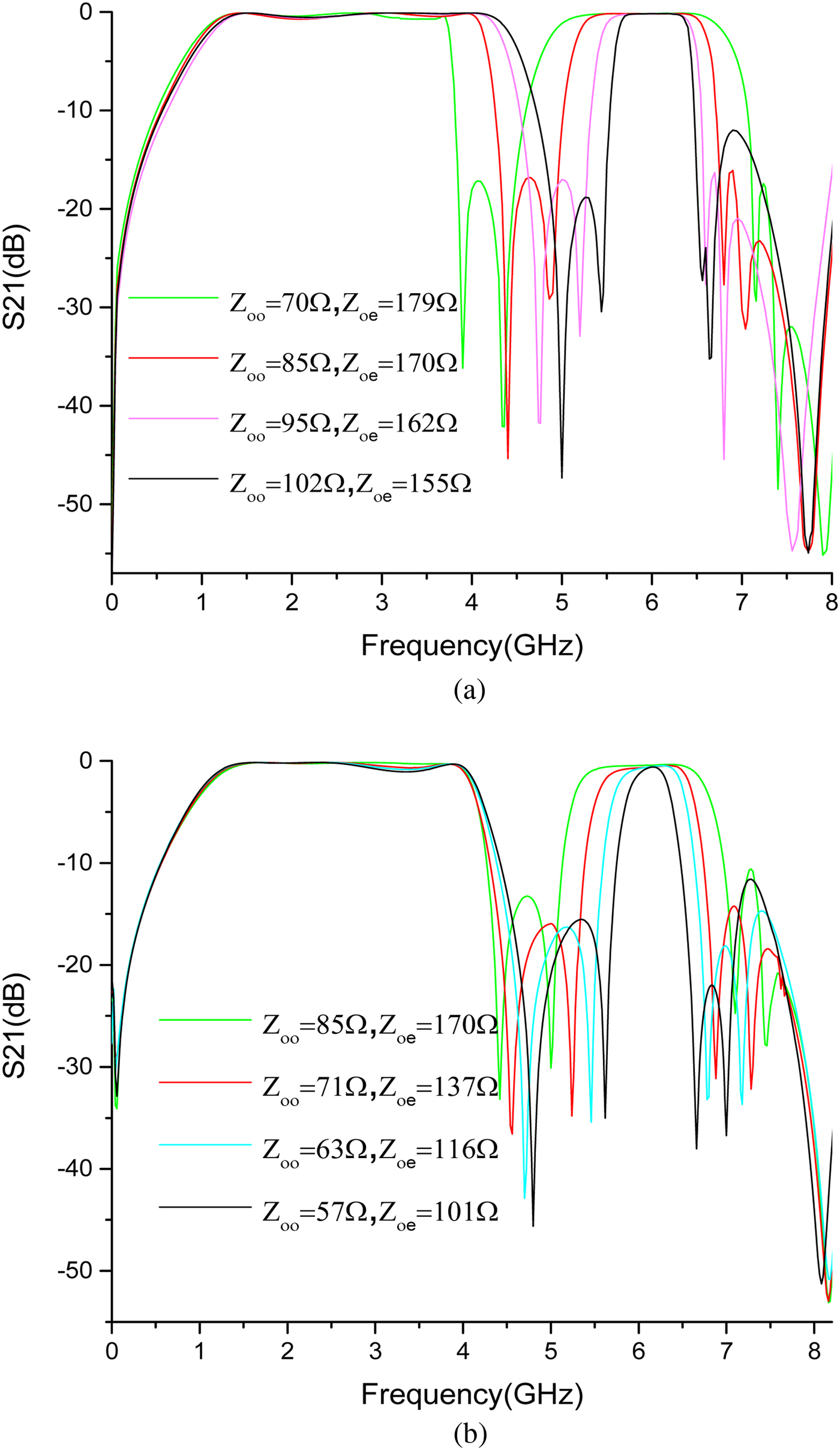
Fig. 7. Transmission coefficients (S 21) response with varied g 1 (a) w 5 (b).
Above all, the key to the design of this filter is to initialize some important parameters like θ 1, θ 2, θ 3, θ c which have influence on the frequency of those two passbands, and Z oo, Z oe which determine the bandwidth. Thus, the design of the filter can be summarized.
(1) The first step is to get the electrical length of θ c in Fig. 3 according to the dual-band filter specification. And then the physical length can be got through θ = ωl.
(2) The second step is to satisfy the bandwidth of the two passbands by adjusting Z oo and Z oe through equations (5 and 6).
(3) The third step is to carry out full-wave electromagnetic simulation and optimization in the commercial software of HFSS so as to guarantee the good in-band flatness and good selectivity.
In this design, the final parameters for the filter circuit of Fig. 1 are Z 1 = 66 Ω, Z 2 = 49 Ω, Z 3 = 121 Ω, Z oo = 85 Ω, Z oe = 170 Ω. The electrical length (deg) of θ 1, θ 2, θ c, and θ 3 are 105, 90, 98, and 140 in 6 GHz, respectively. The center frequencies of the two passbands are located at 2.54 and 5.83 GHz with 3-dB bandwidths of 120 and 28%.
Proposed DWB filter
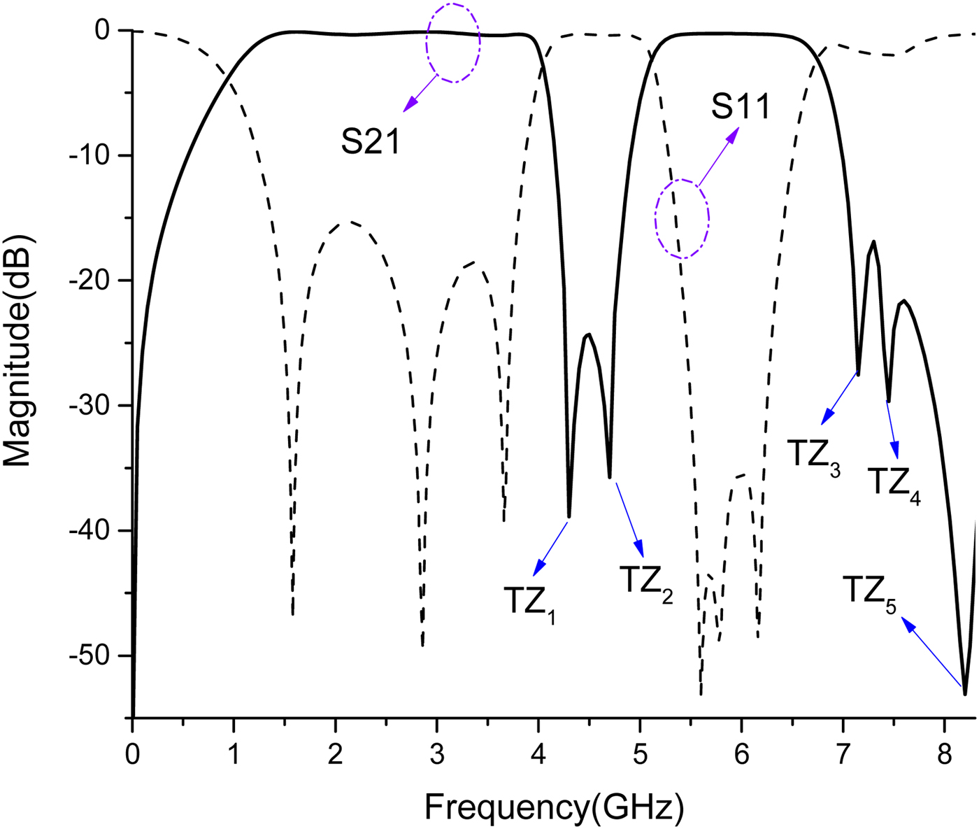
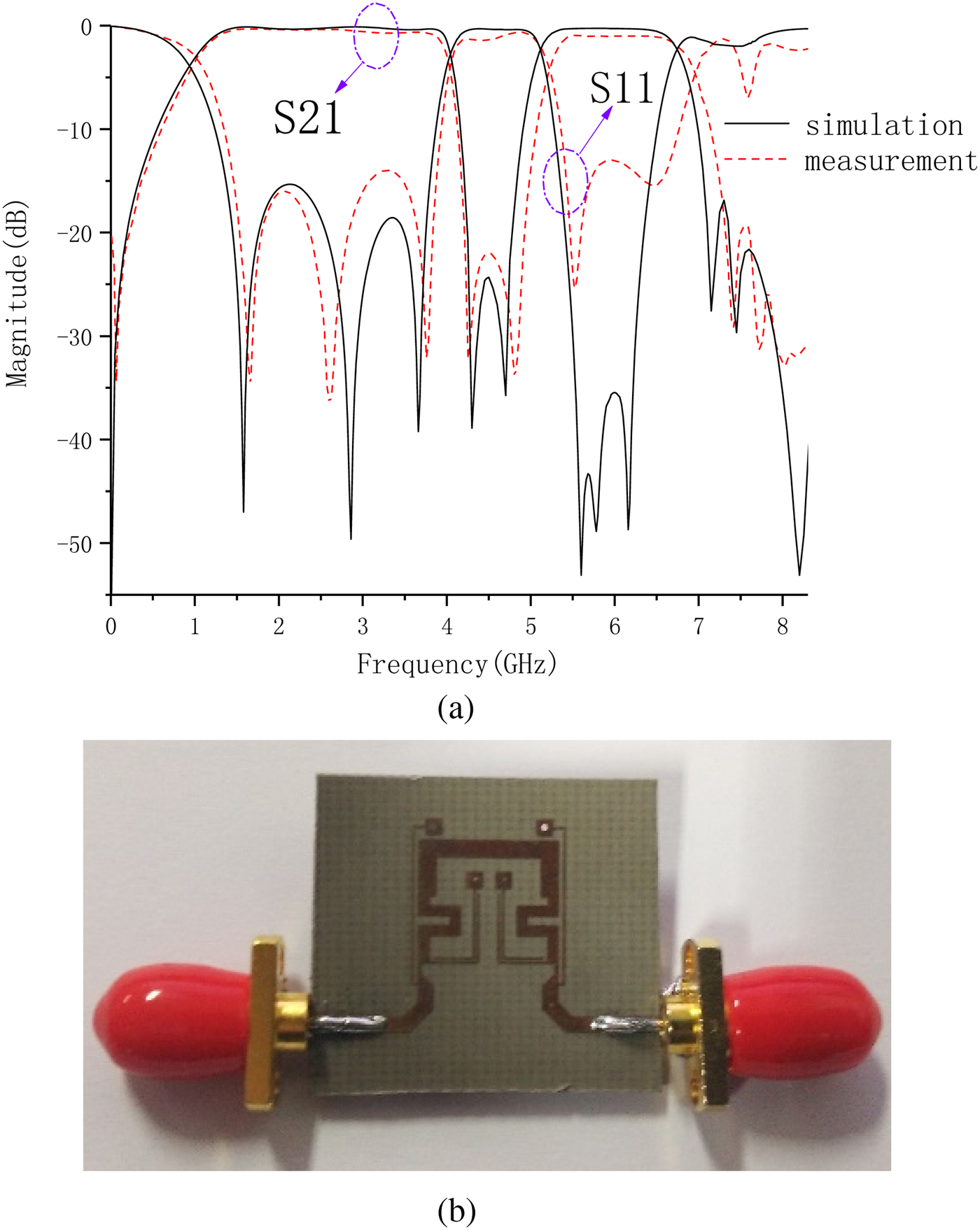
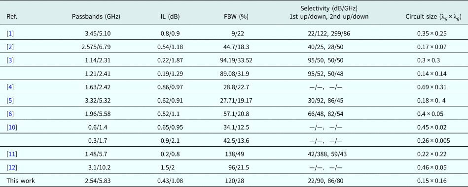
Proposed dual-band BPF was designed and fabricated on a Taconic RF35 substrate as shown in Fig. 1. It has a dielectric constant of 3.5, 0.508 mm thickness and loss tangent of 0.0018. The dimensions of the proposed filter shown in Fig. 1 are as follows: l 1 = 7.4, l 2 = 3.8, l 3 = 9.25, l 4 = 0.55, l 5 = 11.05, l 6 = 0.8, 1 7 = 1.2, l 8 = 0.62, lc 1 = 4.95, lc 2 = 3.5, w 1 = 1.15, w 2 = 0.7, w 3 = 0.15, w 4 = 1.13, w 5 = 0.15, w 6 = 0.27, g 1 = 0.2, g 2 = 1.3, g 3 = 0.3, g 4 = 0.3, all in mm. The photograph of the fabricated BPF is shown in Figs 8(a) and 8(b), and the simulated and measured S-parameters are also shown which demonstrates good agreement for simulation (dashed line) and measurement (solid line). The insertion losses at 2.71 and 6.0 GHz are 0.43 and1.08 dB, respectively. The return losses in the 1st and 2nd band are better than 16 and 13 dB. This filter has −3 dB cut-off frequencies at 1.0–4.15 GHz for the first passband and 5.15–6.8 GHz in the second passband. The filter size is only 0.15λg × 0.16λg, where λg is the guide wavelength for center frequency of the first passband. Five TZ1−5 are at 4.25, 4.75, 7.1, 7.35, and 8.3 GHz. A comparison of the designed dual-band filter to previous works is shown in Table 1, which demonstrates superiority over other designs in insertion loss, bandwidth, selectivity or compactness.

Fig. 8. Simulated and measured results of the proposed filter (a) the photograph (b).
Table 1. Comparison with reported DWB BPFs

Conclusion
This paper has presented a compact DBUWB BPF based on OSCL with detailed design procedure and TZs and TPs analysis. The frequency locations and the bandwidth can be controlled easily. The proposed BPF exhibits a wide bandwidth of 120 and 28% and compact size of 0.15λg × 0.16λgwith a simple coupling scheme and design method, which makes it a good candidate for DWB BPF design. In comparison with other referred filters, the proposed dual-band filter shows wide bandwidth low insertion loss, and compactness.
Acknowledgements
This work was supported by The Ministry of Science and Technology of the People's Republic of China under Grant Number: 2013YQ200503.
 Xiao-Le Bo received B.E. degree from the University of Electronic Science and Technology of China (UESTC), Chengdu, China, in 2016 and now is studying for an M.S. degree in Electromagnetics and Microwave Technology at UESTC. His research interests include electromagnetic theory and microwave circuits and systems.
 Yong-Hong Zhang received B.E., M.S., and Ph.D. degrees from the University of Electronic Science and Technology of China (UESTC), Chengdu, China, in 1992, 1995, and 2001, respectively. From 1995 to 2002, he was a Lecturer with UESTC. From 2002 to 2004, he was a Post-Doctoral Fellow with the Department of Electronic Engineering, Tsinghua University, Beijing, China. Since 2004, he has rejoined UESTC. He is currently a Full Professor with the School of Electronic Engineering. He has authored or coauthored more than 100 internationally refereed journal and conference papers. He is a Senior Member of the Chinese Institute of Electronics. His research interests are in the area of microwave and millimeter-wave technology and applications.
 Xiao-Kun Li received B.E. degree from the University of Electronic Science and Technology of China (UESTC), Chengdu, China, in 2015 and now is studying for a M.S. degree in Electromagnetics and Microwave Technology from UESTC. His research interests include electromagnetic theory and microwave circuits and systems.
 Yang Yang was born in Sichuan Province, China, in June 1989. He received B.S. and M.S. degrees from University of Electronic Science and Technology of China (UESTC), Chengdu, China, in 2011 and 2014, respectively. He is currently working at Sichuan Jiuzhou Electric Co. Ltd. as an engineer. His research interests include microwave and millimeter-wave passive components and control circuits design.
 Yin Tian was born in Sichuan, China. He received M.S. degree from the University of Electronic Science and Technology of China (UESTC), Chengdu, China, in 2007 and is currently working toward a Ph.D. degree at Air Force Engineering University. Since 2007, he has joined the Sichuan Jiuzhou Electric Group Co., Ltd. His research interests include the GaAs/GaN RF integrated circuits design and the phase array T/R module design in microwave and millimeter-wave.
 Yong Fan received B.E. degree from the Nanjing University of Science and Technology, Nanjing, China, in 1985, and M.S. degree from the University of Electronic Science and Technology of China (UESTC), Chengdu, China, in 1992. Since 1989, he has started research and teaching at UESTC. He is currently a Full Professor with the School of Electronic Engineering, UESTC. He has authored or coauthored more than 200 internationally refereed journal and conference papers. He is a Senior Member of the Chinese Institute of Electronics. His main research fields include electromagnetic theory, microwave and millimeter-wave communication, millimeter-wave and Terahertz Circuits etc. Besides, he was interested in other subjects including Broadband Wireless Access, automobile anti-collision, intelligent transportation, etc.