


I. INTRODUCTION
The aim of this contribution is to demonstrate that laboratory-based equipment is able to perform a complex X-ray characterization of heteroepitaxial structures. This is essential for a fast continuous monitoring of deposition processes and for a best possible precharacterization of selected samples, which may be studied in more detail at a synchrotron.
Our subjects of interest are epitaxially grown semiconductor–insulator–semiconductor (SIS) structures. Thin metal oxide (Pr2O3, Y2O3, etc.) layers act as buffer between a Si(111) substrate and the top semiconductor layer of Ge, Si, Si1−xGex, or A3B5 materials. Such structures may be used for new applications in microelectronics (Waser, Reference Waser2003) or in the case of Ge as a possible template for A3B5 material integration (Sheldon et al., Reference Sheldon, Yacobi, Jones and Dunlavy1985). Besides other techniques such as layer transfer, the direct heteroepitaxial growth of SIS structures seems to be a promising way of device preparation (Bojarczuk et al., Reference Bojarczuk, Copel, Guha, Narayanan, Preisler, Ross and Shang2003; Seo et al., Reference Seo, Dieker, Tapponnier, Marchiori, Sousa, Locquet, Fompeyrine, Ispas, Rossel, Panayiotatos, Sotiropoulos and Dimoulas2007). The key problem for this concept of so-called engineered silicon wafers (Fitzgerald, Reference Fitzgerald2005) is the structural perfection of the semiconductor film. To achieve a sufficient perfection, a complex use of different characterization techniques is required in the development of suited deposition techniques.
Here we focus our interest on epi Ge/Pr2O3/Si(111) structures and their characterization by X-ray techniques. Due to different lattice constants, heteroepitaxially grown layers are typically biaxial strained. Different crystal structures, diamond-like for Si and Ge on one side and bixbyite for the oxide on the other side, generate the problem of in-plane orientation of the individual layers relative to each other. A combination of different X-ray techniques will be used to solve the following problems: (a) the in-plane orientation of the oxide and epi-Ge layers relative to the Si substrate; (b) the strain state of both layers; and (c) the crystal perfection especially of the epi-Ge layer.
II. EXPERIMENTAL
The investigated SIS structures were deposited in a multichamber molecular beam epitaxy (MBE) system on 100 mm Si(111) boron doped wafers (see Figure 1). To obtain epi-Ge layers of optimized quality, Pr2O3 buffer layers were grown in a multistep process. It starts with the deposition of hexagonal Pr2O3 on the Si(111) substrate. This layer is transformed by annealing in oxygen to cubic PrO2. In this process, an amorphous Pr silicate layer is formed at the interface of about 2 nm thickness. Regardless of this amorphous layer, the heteroepitaxial relation between the substrate and Pr2O3 generated in the deposition process is preserved. The deposition of epi-Ge is done directly on the PrO2 film, which is hereby reduced to cubic Pr2O3 again. The preparation details are described in Giussani et al. (Reference Giussani, Seifarth, Rodenbach, Müssig, Zaumseil, Weisemöller, Deiter, Wollschläger, Storck and Schroeder2008) and Giussani et al. (Reference Giussani, Rodenbach, Zaumseil, Dabrowski, Kurps, Weidner, Müssig, Storck, Wollschläger and Schroeder2009).
All X-ray measurements were carried out with a Rigaku SmartLab diffractometer using Cu K α radiation in line focus geometry from a 9-kW rotating anode. In the standard X-ray
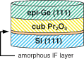
Figure 1. (Color online) Sketch of a heteroepitaxial epi-Ge/Pr2O3/Si(111) stack.
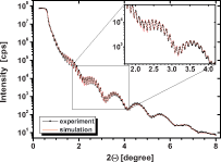
Figure 2. (Color online) XRR measurement and best fitted simulated curve of an epi-Ge/Pr2O3/Si(111) stack.
diffraction (XRD) arrangement the sample is fixed in a horizontal position and the source and detector arm of the diffractometer are moved in a Θ-Θ mode. It is possible to rotate the sample around an axis perpendicular to the sample surface (or adjusted to a nearly surface parallel netplane) defined as angle Φ and to tilt the sample by an angle χ around an axis defined by the beam direction for 2Θ=0°.
Two different resolution schemes were used depending on the measuring technique. In the low resolution (LR) mode, a multilayer X-ray mirror in combination with slit systems is used for beam collimation with or without a flat graphite crystal monochromator in front of the scintillation counter. The beam divergence perpendicular to the diffraction plane was modified by the use of different Soller slit systems on the source and detector arm. The high resolution (HR) mode uses a channel-cut Ge (400) crystal behind the X-ray mirror to collimate and monochromatize the X-ray beam.
Pole figure measurements were carried out in the low resolution mode without a monochromator at a diffraction angle 2Θ fixed to the desired reflection and performing 360° scans in Φ at χ values between 0° and 90°. Soller slits with 0.5° divergence acceptance were used on the source and detector arm, and the step width for Φ and χ of 0.5° was adapted to this. The sample is typically adjusted in such a way that the Φ axis and the normal of the (111) Si substrate netplanes are parallel.
III. RESULTS AND DISCUSSION
The first standard activities to characterize a sample are typically X-ray reflectivity (XRR) and conventional XRD measurements in specular geometry to obtain information about the layer thickness, roughness and density, and about the off-plane orientation of the oxide and epi-Ge layer. Figures 2 and 3 show typical examples for a sample with an 8.5-nm Pr2O3 buffer layer and 82-nm epi-Ge on top. The fitting of the XRR curve with the software RCREFSIMW (IHP, 2009) results in a very good agreement between the experimental and simulated curves (Figure 2). The surface and interface roughness are 0.8 nm and 0.4 nm, respectively. The densities of the epi-Ge and the oxide layer are very close to the expected bulk values.
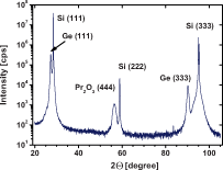
Figure 3. (Color online) Specular Θ/2Θ scan of the same epi-Ge/Pr2O3/Si(111) layer stack as in Figure 2 measured in HR mode.
The conventional specular XRD scan (Figure 3) shows (111) diffraction peaks of different orders n for the Si substrate (n=1,2,3) and for the Ge layer (n=1,3). The broad peak near the forbidden but nevertheless weakly visible Si (222) reflection can be attributed to the Pr2O3 (444) reflection. The lattice constant of cubic Pr2O3 (11.152 Å) is about two times larger than that of Ge (5.657 Å) and Si (5.4309 Å). The Pr2O3 (444) reflection is not forbidden as the Ge (222) reflection. The second and sixth order of the Pr2O3 (111) reflection is superimposed by the first and third order of the (111) reflection of the much thicker Ge layer. The absence of any peak than a (111) reflection confirms that the epi-Ge as well as the Pr2O3 layer have the same (111) off-plane orientation as the Si substrate. The off-plane lattice constant calculated from the Pr2O3 (444) peak position (11.31 Å) is slightly larger than the expected bulk value. This is a first indication for a tetragonal distortion of the Pr2O3 layer. But, this technique gives no information about the in-plane orientation of the oxide and epi-Ge layers relative to the substrate.
The pole figure measurement is a well-known technique for the texture analysis of polycrystalline materials, which is usually not applied for single crystalline substrates with a heteroepitaxial layer on top. But, it turned out that this is a very powerful technique in our case to receive information about the in-plane orientation as well as the structural perfection of the Pr2O3 and epi-Ge layer (Zaumseil and Schroeder, Reference Zaumseil and Schroeder2008). Figure 4 shows three pole figures of different samples. The pole figure of a blanket Si(111) wafer [Figure 4a] exhibits the surface-parallel (111) planes in the central spot. Three additional {111} netplanes 70.5° inclined

Figure 4. (Color online) Pole figures of (111) reflections; (a) measured at a blanket Si(111) substrate wafer (2Θ Si=28.44°), (b) epi-Ge/Pr2O3/Si(111) layer stack (2Θ Ge=27.28°), (c) epi-Ge directly grown on Si(111) (2Θ Ge=27.28°). The intensity covers the range from 1 to 107 cps in logarithmic scale. Spots marked in (b) will be analyzed in more detail.

Figure 5. (Color online) Θ/2Θ XRD scans measured in the spots G 0, G1, O 1, T A, and T B of the pole figure shown in Figure 4b. The vertical lines mark the positions of the Si (111), Ge (111), and Pr2O3 (222) reflections. G 0 and G1 are measured in HR mode; the others in LR mode.
to (111) are visible at Φ=30° (−111), Φ=150° (1-11), and Φ=270° (11-1), respectively. (Φ is counted counterclockwise beginning at the top.) This pattern demonstrates the threefold symmetry of the [111] direction, which is the result of the stacking sequence of the (111) planes in the diamond-like Si lattice. By definition, this is called a type A stacking sequence. If the cubic oxide and epi-Ge lattice have the same in-plane orientation as the Si substrate, any pole figure measured in a (111) reflection would result in a similar intensity distribution. But, the pole figures of the sample with epi-Ge/Pr2O3 layer stack measured with the Ge (111) reflection shows a different situation [Figure 4b].
Besides the same spot pattern characteristic for the Si substrate, there are additional spots visible that are indicating the existence of lattice parts of different orientation. One set of three spots (one of them is marked as O 1) is exactly 180° rotated relative to the substrate spots. Such a 180° rotation around the [111] wafer normal direction is typical for rotation twins representing a type B stacking sequence of the crystal lattice. Furthermore, there are sets of three times three rod-shaped spots visible (one of them is marked as T A) and an additional set of lower intensity spots 180° rotated (T B). These additional spots in the pole figure are obviously representing structural defects either in the oxide or in the epi-Ge layer.
The pole figure shown in Figure 4c demonstrates that an epitaxial growth of Ge directly on Si(111) results in less structural perfection of the epi-Ge layer. It demonstrates that the concept of growing epi-Ge on suitable oxide buffer layers seems to be a promising way to obtain an acceptable quality for technological application.
For a better understanding of the additional features in Figure 4b, XRD scans and reciprocal space maps (RSM) were measured in selected spots. The main conclusions can be drawn from XRD curves summarized in Figure 5. Spot G1 shows the (−111) Si and the (−111) Ge reflections only. This indicates that (at least the main part of) the epi-Ge has the same type A orientation as the Si substrate. The Pr2O3 (−222) reflection, which has nearly the same Bragg angle as the Ge (−111) reflection, is visible in spot O 1 only. Consequently, the oxide layer is completely of type B orientation. But, spot O 1 shows an additional weak peak at the position of the Ge reflection. This results from a small fraction (0.6% in this case) of type B orientation in the epi-Ge layer. The distribution of these type B twins in the epi-Ge layer can be concluded from the ratio between the type B and type A volumes in samples with different layer thicknesses. This ratio decreases with increasing layer thickness, which can be only explained by a preferred location of type B twins near the oxide/Ge interface.
The XRD scans of spot T A and T B in Figure 5 indicate a Ge reflection only. Therefore, the origin of these spots must be from the epi-Ge layer, where significant fractions of the crystal volume must have a different but well-defined orientation. The pole figure spot T A (and T B) is 39° inclined to G 0. The corresponding defect is well known and is usually called

Figure 6. Cross-section (top) and plane-view (bottom) TEM micrographs of an epi-Ge layer with structural defects.

Figure 7. (Color online) Reciprocal space map in spot G 0 at Φ=0° measured in HR mode.
a microtwin. It is the result of a similar 180° rotation twinning as for the type B twins but now the rotation axis is one of the [−111], [1–11], or [11–1] directions, 70.5° tilted relative to the [111] wafer normal. The cross-section TEM micrograph in Figure 6a shows such a defect. Different than typical stacking faults that can also be found in the films, the lamella has a thickness of several atomic layers. Consequently, it is a real volume defect that results in additional {111} plane spots in a pole figure. The microtwins start from the oxide/epi-Ge interface and can reach through the whole layer of type A orientation to the surface. The spots T B are caused by microtwins in Ge grains of type B orientation. Figure 6b shows a TEM plane view of the top layer of a 1 μm thick epi-Ge film.
Type B rotation twins and inclined microtwins are unambiguously detected as observed in pole figure measurements. The microtwins may also contribute to special features of reciprocal space mappings as demonstrated in Figure 7, but the pronounced streaks can also be explained by simple stacking faults lying in inclined {111} planes. The RSM shows the Si and Ge (111) reciprocal lattice points. The Ge reflection has a wide halo of diffuse scattering with two streaks. The stronger one points exactly in the [11-1] direction perpendicular to the (11-1) plane, which includes microtwins and simple stacking faults. The second streak points in the [100] direction. It is most likely that this streak is caused by a superposition and projection of streaks in the [−111] and [1-11] directions into the plane of diffraction. It can be suppressed by reducing the beam divergence perpendicular to the diffraction plane with Soller slits of lower angular acceptance. As a result of annealing experiments we found that the RSM streaks change while the volume fraction of microtwins obtained from pole figure measurements remains constant. This is a clear indication for the existence and possible modification of stacking faults.
The free positioning of our sample in Φ, χ, and 2Θ offers another very interesting possibility to learn more about the detected microtwins. Figure 8 shows a 2Θ-χ mapping measured along two lines in the pole figure with Φ=90° and Φ=30°. The Si and Ge (111) reflections are visible at χ=0°. The O 1 spot with the Pr2O3 (22-2) and the type B Ge (11-1) and the G 1 spot with Si and type A Ge (−111) reflection are visible at χ=70.5° in the left and right parts, respectively. At χ=39°, the T A and T B spots can be found, but they are no isolated spots at χ=39° and 2Θ=27.28°. Rather, the peak shape is characterized by a curved streak starting from the Ge (111) reflection and going far beyond the Si (111) reflection at χ above 45°. This indicates that there exists a more or less smooth transition in the lattice orientation from the Ge matrix to the microtwin accompanied with a modification of the lattice spacing due to the tensile and compressive stress. In connection with Figure 6 one has to keep in mind that the direct intersection of a microtwin as seen in Figure 6a should be considered. They are limited in length and defects of different orientation touch each other [see Figure 6b]. This is all connected with stress and the integral result is seen in Figure 8.
So far the discussion of structural defects was related to the epi-Ge layer only. The question arises, whether it is also possible to get some information about the structural perfection of the Pr2O3 layer. Due to the different in-plane orientation of the Si substrate and epi-Ge on one side and the oxide layer on the other side it is possible to find oxide diffraction spots that are apart from the very small fraction of

Figure 8. (Color online) Intensity vs Bragg angle 2Θ and sample tilt χ measured along a pole figure line with Φ=90° from spots G 0 via T A to O 1 (left) and Φ=30° from spots G 0 via T B to G1 (right). The intensity covers the range from 2 to 2000 cps in logarithmic scale with four lines per decade.

Figure 9. (Color online) Reciprocal space map of spot O 1.
type B Ge free of any other influence. Figure 9 shows the reciprocal space map of the Pr2O3 (22-2) reflection. The Pr2O3 layer of this sample is 8.0 nm thick and buried under 133-nm epi-Ge. Even here it is possible to see streaks of increased diffuse scattering that are definitely related to the Pr2O3 peak and not to the weaker type B Ge reflection. The streak directions can again be explained as projections of different 〈111〉 directions into the plane of diffraction, which indicates that inclined {111} planes are also for the oxide preferred locations of structural defects. In fact, this measurement represents the limit for the laboratory-based technique. The measuring time was about 60 h. Synchrotron measurements are absolutely required for further characterization of such thin layers.
The main structural features of the investigated epi-Ge/Pr2O3/Si(111) layer stack discussed above are summarized in Figure 10. It shows a stacking sensitive cut through the crystal lattice in a plane given by the [111] and [11-2] directions. The oxide and epi-Ge layers have the same [111] orientation perpendicular to the surface as the Si substrate. The stacking sequence of the Si substrate and the majority of the epi-Ge layer are of type A. A small part of the epi-Ge and the whole oxide layer show a type B stacking. The major type of structural defects in the type A and type B grains of the epi-Ge layer are microtwins (shown for type A only). The (111) lattice planes inside the thin lamella are 39° inclined to the corresponding planes of the matrix, which generates the T A spot. From TEM studies we know that the

Figure 10. Sketch of the main structural features of the investigated epi-Ge/Pr2O3/Si(111) layer stack.
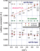
Figure 11. (Color online) Measured lattice constants of Si, Ge, and Pr2O3 vs cos2χ (top), and a more detailed analysis of the Ge reflections (bottom). For better comparison, the lattice constant of Pr2O3 is divided by 2.
microtwins have a thickness of up to ten atomic layers. The bold line parallel to the microtwin in the epi-Ge layer indicates the existence of stacking faults. Similar structural defects exist in the thin Pr2O3 layer.
The existence of different stacking types in one stack of heteroepitaxial layers opens completely new possibilities to analyze the lattice parameters of individual layers or parts of one layer. In Figures 4 and 5 it was demonstrated that diffraction spots of type A and type B lattices occur at different positions in the pole figure and can thus be analyzed without any superposition. The same situation exists with only few exceptions for all reflections. Thus, it is possible to measure the plane distance of type A and type B reflections independently by Θ/2Θ scans at well-defined diffractometer parameters Φ and χ. The strain state of the oxide and epi-Ge layers can be analyzed by a technique described by Zaumseil (Reference Zaumseil2008), where a theoretical cubic lattice constant calculated from the peak position of different inclined reflections is plotted vs the cosine square of the tilt angle χ. The resulting straight line gives the in-plane lattice constant at cos2χ=0 and the off-plane lattice constant at cos2χ=1. This technique is comparable to the sin2Ψ method to measure the strain in polycrystalline samples, but here different Bragg reflections under various tilt angles are used. Figure 11 shows the results of such an analysis for a sample with 180-nm epi-Ge on an 8.5 nm thick Pr2O3 buffer layer in the as-grown state and after annealing at 825 °C for 30 min in UHV.
The off-plane lattice constant of the as-grown oxide layer (11.288 Å) is distinctly larger than the in-plane lattice constant (10.989 Å), which indicates that this layer is compressively strained. The annealing procedure has no significant influence on the oxide strain. A more detailed analysis of the epi-Ge layer in Figure 11b is surprising at first view. Growing a not fully relaxed material on a substrate with a smaller in-plane lattice constant results typically in compressive strain. The observed tensile strain can be explained under the assumption of full relaxation by the difference in the linear coefficients of the thermal expansion of the Si substrate
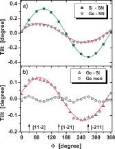
Figure 12. (Color online) (a) Tilt of the (111) netplanes of Si substrate and epi-Ge relative to the surface normal (SN). (b) Tilt of the Ge relative to the Si lattice and the difference of this curve to a fitted sinusoidal function.
and epi-Ge layer acting during the cooling from Ge growth (550 °C) down to room temperature (Hartmann et al., Reference Hartmann, Papon, Destefanis and Billon2008). This effect is increased by annealing at a higher temperature (825 °C).
Finally we analyzed the tilt of the (111) netplanes of the epi-Ge and Si substrates relative to the wafer surface and to each other. To do this, the sample was adjusted with the surface normal parallel to the Φ axis. The tilt of the (111) netplanes relative to the surface was measured as a function of Φ. It is calculated as the difference between the peak position of a Θ scan carried out at a fixed 2Θ position of the corresponding Bragg peak and one half of this 2Θ value.
Results are shown in the upper part of Figure 12. Fitting with the expected sinus function results in a tilt of 0.33° for the Si substrate (a typical value for production wafers) and 0.13° for the epi-Ge layer. The netplane tilt relative to the surface is obviously reduced by the oxide layer and the following epi-Ge layer. This effect is well known for strained epilayers on miscut substrates. For relaxed layers it is explained by the preference of the slip system in the direction of the miscut over the other (Nagai, Reference Nagai1974; Riesz et al., Reference Riesz, Lischka, Rakennus, Hakkarainen and Pesek1991; Hess et al., Reference Hess, Moore and Goorsky1999). The lower part of Figure 12 shows the tilt of the epi-Ge relative to the Si substrate. It is obvious that there exists a periodic modulation between the measuring points and the fitted sinusoidal function. The differential curve can be fitted again with a sinusoidal curve but now with a periodicity of 120° and amplitude of 0.017°. The maxima correlate to the in-plane directions that agree with the projection of the directions normal to the tilted and microtwin containing (111) planes into the wafer plane. This shows that the threefold symmetry of the defect generation favored in the inclined (111) planes also has an influence on the flatness of the nearly surface parallel (111) netplanes.
IV. SUMMARY AND OUTLOOK
It was shown that a complex characterization of heteroepitaxial semiconductor– insulator–semiconductor structures is possible by a combination of different laboratory-based X-ray techniques. This was demonstrated for epi-Ge/Pr2O3/Si(111) layer stacks. Especially the combination of X-ray pole figure measurements with reciprocal space mapping and high resolution Θ/2Θ scans at selected inclined netplanes can be used successfully to determine the in-plane lattice orientation of the layers relative to the substrate, the strain state of all layers, and the structural perfection of the epi-Ge and oxide buffer layers.
It was demonstrated that the main part of the epi-Ge layer has the same type A stacking orientation as the Si substrate, but about 0.6% is of type B. The Pr2O3 buffer layer exhibits type B only. The oxide layer is tetragonal distorted due to compressive stress, while the epi-Ge layer is fully relaxed and shows a weak tensile strain explained by the action of different linear coefficients of the thermal expansion of the Si substrate and epi-Ge layer during cooling down from deposition to room temperature. Furthermore, it was found that microtwins lying in inclined {111} planes are the dominating structural defects in the epi-Ge layer. They generate a characteristic scattering pattern in reciprocal space maps, but the unambiguous identification was done by pole figure measurements. It was found that the tilt of (111) planes relative to the wafer surface decreases from the Si substrate to the epi-Ge layer, where the well-defined defect orientation causes a periodic in-plane variation of the mean (111) layer plane tilt.
This contribution was mainly focused on the methodical aspects of the X-ray characterization of SIS structures and not primarily on material features. The use of laboratory-based equipment offers the possibility of a fast and near-preparation analysis of samples required for an improvement and optimization of the deposition process. Besides the discussed epi-Ge/Pr2O3/Si(111) layer stacks, this methodology was successfully used for the characterization of epi-Si/Y2O3/Pr2O3/Si(111) (Zaumseil et al., Reference Zaumseil, Giussan, Seifart, Arguirov, Schubert and Schroeder2009), lattice matched epi-Si/Y2−x PrxO3/Si(111), and other heteroepitaxial systems. The density of structural defects in the top semiconductor layer is on the order of 109 cm−2, which is definitely too high for microelectronics applications. It was found that postdeposition annealing is able to improve the layer perfection, but the most promising way for a significant defect reduction seems to be a further optimization of the deposition conditions.
Using the described techniques a complex precharacterization of samples is possible that will be studied in more detail by synchrotron measurements. For example, the position of rotation twins at the oxide/epi-Ge interface was concluded in a rather indirect way from samples of different epi-Ge layer thicknesses. This was proved for epi-Si on Y2O3/Pr2O3 buffer in a more direct way by synchrotron radiation grazing incidence diffraction measurements under different incident angles (Schroeder et al., Reference Schroeder, Zaumseil, Seifarth, Giussani, Müssig, Storck, Geiger, Lichte and Dabrowski2008). Furthermore, synchrotron radiation measurements are in progress to study the diffuse scattering of structural defects in the top semiconductor and the oxide buffer layer to learn more about the fundamental aspects of defect generation and interaction in such structures.


