


1. INTRODUCTION
For the modulation signal with a high peak-to-average power ratio (PAPR), the transmitter should be operated at a backed-off average output power region for an acceptable linearity, resulting in a low-efficiency characteristic. However, a high efficiency with high linearity is essential for a low-cost wideband transmitter. To achieve both the requirements at the same time, a combined architecture of an efficiency enhancement technique and a linearization technique should be developed. As a linearization technique, the digital predistortion (DPD) shows a very powerful and reliable linearization capability and is the favored method for the linearization of the base-station amplifier [Reference Woo1]. As an efficiency enhancement technique, the hybrid envelope elimination and restoration/envelope tracking technique (H-EER/ET) and the Doherty technique can be considered [Reference Doherty2–Reference Choi, Kang, Kim, Park and Kim9]. Recently, these two techniques delivered an excellent efficiency performance. In the H-EER/ET transmitter, the power amplifier (PA) is driven to the saturated state by the modulated input signal, and the drain bias of the PA is modulated by the optimum envelope signal through the efficient bias modulator. Owing to the saturated operation along the whole output power level, highly efficient operation can be expected, and high linearity can be achieved theoretically by the separated restoration mechanism of the amplitude and phase information [Reference Kimball7, Reference Kim, Kim, Moon and Kim8]. But the H-EER/ET transmitter is not implemented for the mass production at the industry yet owing to difficulties such as efficiency and bandwidth enhancement of the bias modulator and complexity of the circuit compared to the other PAs. On the other hand, the Doherty technique is not an optimum architecture in terms of efficiency for amplification of a high-PAPR signal, because the efficiency degradation region exists at the low-power region and the unsaturated peaking PA's operation region [Reference Raab3, Reference Cripps10]. In spite of this imperfection, the Doherty PA has been delivering the highest efficiency among various PAs because of the well-developed simple circuit. Accordingly, the Doherty PA market has experienced rapid growth in recent years [Reference Deguchi, Ui, Ebihara, Inoue, Yoshimura and Takahashi11].
In this paper, by considering the distribution of a PA's power generation probability for the modulation signal [Reference Pelk, Neo, Gajadharsing, Pengelly and de Vreede12], we have verified that the most efficient Doherty architecture for a high-PAPR signal is the 3-stage Doherty PA. For a highly efficient operation at the backed-off output power region, while maintaining the peak power, we optimized the “ET” 3-stage Doherty PA by using Matlab simulation. The unit PA has been designed using a saturated mode PA to maximize the Doherty PA's efficiency. The 5 W and two 10 W PEP LDMOSFETs are employed for the 802.16e mobile world interoperability for microwave access (WiMAX) signal with 8.5 dB PAPR at 1 GHz.
II. Comparison of N-way versus 3-stage Doherty PA
As reported in many papers [Reference Raab3, Reference Yang, Cha, Shin and Kim13], the ‘N-way’ Doherty PA has two maximum efficiency points at the backed-off output power and the peak power, respectively. The back-off level for the first maximum efficiency, 20 log(1/N) [dB], is determined by selecting the peaking PA's size. On the other hand, the ‘3-stage’ Doherty PA has three maximum efficiency points along the output power level [Reference Neo, Qureshi, Pelk, Gajadharsing and de Vreede14]. The back-off levels with the two maximum efficiencies are determined by the two peaking PAs' size ratio compared to the carrier PA, which is derived in [Reference Pelk, Neo, Gajadharsing, Pengelly and de Vreede12], 20 log(k 1)[dB] and 20 log(k 2) [dB]. The k 1 and k 2 are the input power back-off points on the normalized input voltage magnitude. In Table 1, the back-off levels of various Doherty PAs are summarized. In Fig. 1, the efficiency characteristics of various Doherty PAs are illustrated when all the PAs are biased at the class B mode in the ideal condition. There are four kinds of 3-stage Doherty PA and two kinds of N-way Doherty PA with different size ratios between the carrier PA and peaking PAs. The 3-stage Doherty PAs maintain relatively flat and high efficiency along the output power level because of the three maximum efficiency characteristics compared to those of the N-way Doherty PA. To evaluate the average efficiency of each Doherty PA for the 802.16e mobile WiMAX signal with 8.5 dB PAPR, the efficiency is calculated using the following equation [Reference Hanington, Chen, Asbeck and Larson15]:

Fig. 1. The efficiency characteristics of various Doherty PA versus the normalized output power.
Table 1. The back-off level and average efficiency of the ‘N-way’ and ‘3-stage’ Doherty PAs for the 802.16e Mobile WiMAX signal with 8.5 dB PAPR

The prob.(V in) is the probability of occurrences at V in for the modulated input signal. In this equation, the overall DE is determined by the multiplication of the probability distribution and the power generation terms (P out) at the distribution over the DC power (P dc). The numerator of the above function (probability × power) is named the power generation distribution (PGD) of the Doherty PA [Reference Kim, Woo, Kim, Moon, Kim and Kim6]. The distribution indicates the important power generation region for the Doherty operation, and the operation at the region determines the average efficiency. In Fig. 1, PGD is also depicted, and the 3-stage Doherty PA maintains the high-efficiency characteristic broadly at the important operation region, while the N-way Doherty PAs do not. In Table 1, the calculated average efficiencies of each Doherty PA for the WiMAX signal are presented, and the 3-stage Doherty PAs have shown about 10% improved efficiency compared to the N-way Doherty PAs. It is clearly shown that the 3-stage Doherty PA is the most efficient architecture for amplification of the WiMAX signal with 8.5 dB PAPR.
The peaking PAs of the N-way Doherty PA are biased at a class C mode for the proper turn-on operation at the required output power level, and the carrier PA should be driven into hard saturation to achieve its peak power. The peaking PAs of the 3-stage Doherty architecture are turned on one after the other and it is in the worse situation because the PA's gate bias is lower than that of the N-way Doherty case. Thus, the load cannot be modulated completely at the peak power region, even worse than the N-way Doherty. Because of the incomplete load modulation, we cannot achieve high efficiency and high peak power simultaneously. Therefore, we have to select one of the two design cases. One is the peak power and flat gain response (linear amplitude modulation-amplitude modulation(AM-AM)) with the poor efficiency at backed-off output power region. The other case is a high efficiency at the backed-off output power level with an insufficient peak power and gain flatness. Both the selections are not the optimum design. To overcome this problem, we may employ the uneven input power drive technique [Reference Kim, Cha, Kim and Kim16], but it reduces the linear gain. Moreover, the load modulation is not enough to achieve high efficiency at the backed-off output power level and the peak power at the same time. The other alternative is the gate bias control of the peaking PAs [Reference Yang, Cha, Shin and Kim17, Reference Moon, Kim, Kim, Kim and Kim18]. Generally, the gate bias control of the Doherty PA has been employed for the IM cancelation. In this paper, we have investigated the peaking PA's gate bias control of the 3-stage Doherty PA for efficiency improvement at the backed-off output power level and the peak power at the same time besides linearization. The architecture of the proposed 3-stage Doherty PA is shown in Fig. 2.

Fig. 2. The architecture of the proposed ET 3-stage Doherty PA.
III. Analysis of the proposed 3-stage Doherty PA
A. Conduction angle of each PA versus input voltage magnitude
We conducted the Matlab simulation to analyze the operation of the 3-stage Doherty PA with and without the gate bias control. For exact modeling of the peaking PA operation, we used the fundamental and DC current components derived by the conduction angle versus the input voltage magnitude as shown in Fig. 3. The RF current waveform can be defined as [Reference Cripps10]

where I q is the quiescent bias current and I pk(v in) is the magnitude of the drain current of the given PA. We assume that all the PAs have a constant gm versus input voltage for simplicity. The final conduction angle versus input voltage magnitude can be derived as [Reference Colantonio, Giannini, Giofre and Piazzon19]
![\eqalign{\therefore \alpha_{vin} & = 2 \cdot arccos \left[{V_{gsq}\over V_{gsq}- \lpar v_{in}/V_{MAX} \rpar }\right] \cdot {180\over \pi} \cr & \quad \hbox{where} \comma \, cos \lpar \alpha_{vin}/2 \rpar = -{I_{q}\over I_{pk} \lpar v_{in} \rpar } \comma \cr &\quad I_{pk} \lpar v_{in} \rpar = Iin \lpar v_{in} \rpar -I_{q}. }](https://static.cambridge.org/binary/version/id/urn:cambridge.org:id:binary:20160921015651061-0137:S1759078710000711:S1759078710000711_eqn3.gif?pub-status=live)

Fig. 3. The conduction angle variation versus the input power level with different bias: (a) Class AB mode and (b) Class C mode. (The I ds below 0 is the cut-off level.)
The I in (v in) is an absolute amplitude of the drain current under the given input voltage, ‘v in’, and it is proportional to the input voltage. Therefore, the fundamental and DC currents of the carrier and two peaking PAs based on each conduction angle can be defined as follows:
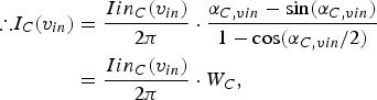


![\alpha_{C \comma vin} = \left\{\matrix{ 2 \cdot arccos \left[\displaystyle{V_{gsq \comma C}\over V_{gsq \comma C}-v_{in}/ \lpar k_{1} \cdot V_{MAX} \rpar } \right] \comma \hfill \cr \qquad \qquad \qquad 0 \lt \displaystyle{{v_{in}\over V_{MAX}}} \lt k_{1}, \hfill \cr 2 \cdot arccos \left ( \displaystyle{V_{gsq \comma C}\over V_{gsq \comma C}-1} \right ) \comma \hfill \cr \qquad \, k_{1} \lt \displaystyle{v_{in}\over V_{MAX}} \lt 1 \comma }\right.](https://static.cambridge.org/binary/version/id/urn:cambridge.org:id:binary:20160921015651061-0137:S1759078710000711:S1759078710000711_eqnU1.gif?pub-status=live)
B) Efficiency of the 3-stage Doherty PA
If all the PAs are matched to the load impedance, R L, at the full-power state, the characteristic impedance of the output combiner can be selected as [Reference Pelk, Neo, Gajadharsing, Pengelly and de Vreede12]

For the ease of device selection, a ‘1:2:2’ (1: m 1:m 2) 3-stage Doherty PA has been investigated. Thus, k 2 and k 1 are determined to be 0.33 and 0.6, respectively, on the v in/V MAX axis. At the region of ‘0 ~ k 2’, only the carrier PA is operated, and at the region of ‘k 2 ~ k 1’, the carrier and peaking PA 1 are operated. All the PAs are turned on at the region of ‘k 2 ~ 1’ on the axis.
The ideal current source expression of the 3-stage Doherty PA at the region of ‘0–0.33’ is shown in Fig. 4(a). The load impedance at the carrier PA's current source can be derived as


Fig. 4. The ideal current source expression of the 3-stage Doherty PA: (a) second back-off region, (b) first back-off region and (c) full-power condition. (Black: turn on state; gray: turn off state.)
The drain efficiency below the second back-off region can be calculated using the RF power and DC power,
where
Fig. 4 (b) represents the region of ‘0.33–0.6’, where the carrier PA and peaking PA supply the fundamental currents to the load. The fundamental drain current ratio between the carrier PA and peaking PA 1 is defined as
The load impedance at each voltage node can be calculated using the active load-pull principle [Reference Cripps10].

![\therefore R_{C \comma \sim k_{1} \lpar v_{in} \rpar } = {Z_{01}^2 \cdot Z_{03}^2\over Z_{02}^2 \cdot R_{L} \cdot [1+\delta_{1 \lpar v_{in} \rpar }]} \comma](https://static.cambridge.org/binary/version/id/urn:cambridge.org:id:binary:20160921015651061-0137:S1759078710000711:S1759078710000711_eqn15.gif?pub-status=live)
![\therefore R_{P1 \comma \sim k_{1} \lpar v_{in} \rpar } = \left[1+ {1\over \delta_{1 \lpar v_{in} \rpar }} \right] \cdot {Z_{02}^2\over Z_{01}^2} \cdot R_{L}.](https://static.cambridge.org/binary/version/id/urn:cambridge.org:id:binary:20160921015651061-0137:S1759078710000711:S1759078710000711_eqn16.gif?pub-status=live)
The drain efficiency below the first back-off region can be calculated in the same way.
![\eqalign{\therefore DE_{\sim k_{1} \lpar v_{in} \rpar } &= {1\over 4\pi \cdot R_{L} \cdot I_{max \comma C}} \cdot [Iin_{C} \lpar v_{in} \rpar ^{2} \cdot W_{C}^{2} \cdot R_{C \comma \sim k_{1} \lpar v_{in} \rpar }\cr &\quad +Iin_{P1} \lpar v_{in} \rpar ^{2} \cdot W_{P1}^{2} \cdot R_{P1 \comma \sim k_{1} \lpar v_{in} \rpar }] /\cr &\quad [Iin_{C} \lpar v_{in} \rpar \cdot Y_{C} + m_{1} \cdot Iin_{P1} \lpar v_{in} \rpar \cdot Y_{P1}] \comma }](https://static.cambridge.org/binary/version/id/urn:cambridge.org:id:binary:20160921015651061-0137:S1759078710000711:S1759078710000711_eqn17.gif?pub-status=live)
where

Fig. 4(c) represents the region of ‘0.6–1’, where all the PAs' current sources supply the fundamental current to the load. The fundamental drain current ratio between the carrier PA and two peaking PAs is defined as
The load impedance at each voltage node can also be calculated in the same way:
![\therefore R_{P2 \comma \sim 1 \lpar v_{in} \rpar } = \left[1 +{1\over \delta_{2 \lpar v_{in} \rpar }} \right] \cdot {Z_{01}^2\over R_{L}} \comma](https://static.cambridge.org/binary/version/id/urn:cambridge.org:id:binary:20160921015651061-0137:S1759078710000711:S1759078710000711_eqn20.gif?pub-status=live)
![\therefore R_{T3 \lpar v_{in} \rpar } = {Z_{02}^2 \cdot R_{L}\over Z_{01}^2 \cdot \left[1+\delta_{2 \lpar v_{in} \rpar } \right]}](https://static.cambridge.org/binary/version/id/urn:cambridge.org:id:binary:20160921015651061-0137:S1759078710000711:S1759078710000711_eqn21.gif?pub-status=live)

![\therefore R_{P1 \comma \sim 1 \lpar v_{in} \rpar } = {Z_{02}^2 \cdot R_{L}\over Z_{01}^2} \cdot {1+\delta_{1 \lpar v_{in} \rpar }\over \delta_{1 \lpar v_{in} \rpar } \cdot\left[ 1+\delta_{2 \lpar v_{in} \rpar } \right]}.](https://static.cambridge.org/binary/version/id/urn:cambridge.org:id:binary:20160921015651061-0137:S1759078710000711:S1759078710000711_eqn23.gif?pub-status=live)
The drain efficiency up to the full-power state can be calculated using the RF power and DC power,
![\eqalign{\therefore DE_{\sim 1 \lpar v_{in} \rpar } &= {1\over 4\pi \cdot R_{L} \cdot I_{max \comma C}} \cdot [Iin_{C} \lpar v_{in} \rpar ^{2} \cdot W_{C}^{2} \cdot R_{C \comma \sim 1 \lpar v_{in} \rpar } \cr &\quad + Iin_{P1} \lpar v_{in} \rpar ^{2} \cdot W_{P1}^{2} \cdot R_{P1 \comma \sim 1 \lpar v_{in} \rpar } \cr & \quad + Iin_{P2} \lpar v_{in} \rpar ^{2} \cdot W_{P2}^{2} \cdot R_{P2 \comma \sim 1 \lpar v_{in} \rpar }] /\cr &\quad [Iin_{C} \lpar v_{in} \rpar \cdot Y_{C} + m_{1} \cdot Iin_{P1} \lpar v_{in} \rpar \cdot Y_{P1} \cr &\quad + m_{2} \cdot Iin_{P2} \lpar v_{in} \rpar \cdot Y_{P2}] \comma }](https://static.cambridge.org/binary/version/id/urn:cambridge.org:id:binary:20160921015651061-0137:S1759078710000711:S1759078710000711_eqn24.gif?pub-status=live)
where

C) Matlab simulation results of the 3-stage Doherty PA with and without adaptive gate ET operation
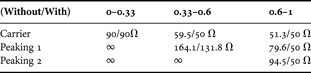
For simulation, the conduction angle of the carrier PA at the full-power state is set to 180° (V gsq,C = 0), and those of the peaking PAs to 151.05° (V gsq,P1 =−0.33) and 135.95° (V gsq,P2 = −0.6) to turn on the PAs above the k 2 and k 1, respectively. The 3-stage Doherty PA simulated is configured to ‘1:2:2’ unit PAs, and the drain DC bias applied is 30 V. In Fig. 5, the optimum gate bias shapes versus the normalized input voltage magnitude are illustrated, and the biases are increased from the class C mode to enhance the output power of each peaking PA as the input power level is increased. In Fig. 6, the simulation results of the 3-stage Doherty PA with and without the gate adaptation to the peaking PAs. Fig. 6(a) shows the simulated fundamental drain current increment of each PA [Reference Smith, Eccleston, Gough and Mann20]. Without the gate bias adaptation, the fundamental drain currents of the peaking PA 1 and 2 do not reach the 2 A (which is two times larger magnitude than the carrier PA's maximum drain current) because of the low gate bias. Fig. 6(b) shows the fundamental drain voltage variation versus the normalized input voltage. As expected from Fig. 6(a), the two peaking PAs' drain voltage do not reach 30 V. Especially, the peaking PA 2's fundamental current and voltage show the seriously insufficient load modulation. The load impedance variation at each current source is presented in Fig. 6(c) and Table 2. All PAs do not reach the required load impedance after the ‘0.33’ of the normalized input power level. The fundamental drain current ratios, δ1 and δ2, have to be increased from 0 to 2 and from 0 to 0.6, respectively. The variation of the δ1 and δ2 are shown in Fig. 6(d). The optimum gate biases of each peaking PA are determined to get the proper load impedances which decide the efficiency and output power(or gain flatness) of Doherty PA versus the input voltage level. At the region of ‘0.33–0.6’ on the normalized input voltage axis, only the peaking PA 1's gate biases is increased. As the peaking PA 1's gate bias is increased, the fundamental drain voltage of the PA reaches the 30 V, and the load impedance is converged to ‘2.5·Ro’ of load impedance in Fig. 6(a) and (b). At the region of ‘0.6–1’, both the peaking PAs' gate biases have to be adapted. Through the gate bias adaptation, the two peaking PAs' fundamental drain currents reach its maximum magnitude, and the carrier PA and peaking PA 1's fundamental drain voltages are maintained near the 30 V. The load impedances of all PAs are converged to the 50 Ω, and the proper load modulation behavior is achieved along the overall input power level. The δ1 and δ2 are also enhanced to 2 and 0.6, respectively.

Fig. 5. The optimum gate bias shapes for the peaking PAs versus the normalized input voltage.

Fig. 6. The simulation result of the ‘1:2:2’ 3-stage Doherty PA with and without the gate bias adaptation(GA): (a) fundamental drain currents, (b) fundamental drain voltage, (c) fundamental load impedance at the each current source, and (d) the calculated δ1 and δ2.
Table 2. The load impedance variation versus the input power level for the ‘1:2:2’ 3-stage Doherty PA with and without the gate bias adaptation
In Fig. 7(a), the simulated load lines of each PA are illustrated, only showing the left side from V DC of 30 V, for simplicity. As shown in figure, without the gate control, the minimum drain voltages of the peaking PAs do not reach the knee region. This operation causes serious degradation of efficiency for the two peaking PAs, and the overall efficiency of Doherty PA is decreased at the backed-off output power region as shown in Fig. 7(b). Therefore, the optimum gate bias has to be properly shaped such that the carrier PA and peaking PA 1's fundamental drain voltages maintain 30 V. In this simulation, for simplicity, the two peaking PAs' fundamental drain currents along the power level are the same with the fundamental drain current shapes of the class C mode single PAs, whose conduction angles are 151.05° and 135.95°, respectively. Without the gate control, the peaking PAs do not reach the knee region because of the improper load modulation. The improper load modulation also reduces the peak power by about 3.33 dB as shown in Fig 7 (b). Furthermore, the two peaking PAs are also of low efficiency at the backed-off output power region. The simulated gain flatness versus the output power level is depicted in Fig. 7(c). The calculated gain flatness is improved from 3.8 to 1 dB after applying the gate bias control technique, indicating more linear AM–AM response of the proposed PA.

Fig. 7. The simulated (a) fundamental load-line behavior, (b) efficiency characteristic, and (c) gain characteristic of the ‘1:2:2’ 3-stage Doherty PA with and without the gate bias adaptation.
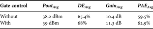
In Fig. 8, the calculated DC and RF powers of each PA and the overall are illustrated. By applying the gate bias control technique, the RF power generation of the two peaking PAs are enhanced significantly, and the 3-stage Doherty PA properly delivers the full power to the load. In Table 3, the calculated average performance of the 3-stage Doherty PA with and without the gate bias control technique are summarized for the WiMAX signal with 8.5 dB PAPR. The proposed Doherty PA shows an enhanced efficiency together with an improved average output level. These simulation results clearly show the limitation on the load modulation behavior of the conventional 3-stage Doherty PA, and the limitation can be removed by the gate bias control technique.

Fig. 8. The simulated DC, RF powers of each PA and total power (a) without and (b) with the gate bias adaptation.
Table 3. The calculated average performance of the 3-stage Doherty PA with and without applying the gate bias control technique for the 802.16e Mobile WiMAX signal with 8.5 dB PAPR.
IV. Implementation and Measured Results
A) Class F−1 PA for the unit cell
To maximize the efficiency of the proposed 3-stage Doherty PA, we have employed a class F−1 PA as an unit cell shown in Fig. 9 [Reference Kim, Moon, Woo, Hong, Kim and Kim21]. The harmonic control circuit provides an open impedance at the second harmonic and a short impedance at the third harmonic. The harmonic control impedances are provided at the drain current node inside of the intrinsic capacitive components and the packing elements. Accordingly, the control circuit includes both-arm shunt stubs for better harmonic trap and tuning lines to compensate the de-tuning effects of the device's parasitic passive components [Reference Woo, Yang and Kim22]. The output matching network has been designed considering the impedance mismatch by the non-linear capacitive components. We have implemented the PAs using 5 W PEP MRF281S and 10 W PEP MRF282S LDMOSFETs and the quiescent gate bias voltages of each PA are 3.2 and 3.4 V, a class B mode, respectively, under the 30 V of a drain bias at 1 GHz. The unit PA for the carrier PA has a 71.3% of drain efficiency at an output power of 38.7 dBm, and the PA for the peaking PA has been obtained as 71.4% of drain efficiency at an output power of 41.6 dBm. The PA's output impedance for the peaking PA is measured to be 652 Ω after the offset line (phase offset = 92.9°).

Fig. 9. The implemented circuit topology of the class F −1 PA.
B) Measured results for the CW signal
Fig. 10 shows the measured optimum gate bias control shapes versus the input power level. A constant gate bias is applied to the carrier PA. The gate biases of the other PAs are maintained at a deep class C mode initially for the completely turned-off operation. Above each backed-off average output power, each PA's gate biases are increased to the class B mode to accelerate the load modulation. To investigate the load modulation behavior with and without applying the gate bias control technique, the output power of the 3-stage Doherty PA and the DC current profiles of each PA versus the input voltage are measured and depicted in Fig. 11. When the proposed Doherty PA reaches the peak power of 28.4 W, the Doherty PA without the gate bias adaptation generates a 10.5 W of output power. To achieve the same peak power from the latter Doherty PA, an almost two times larger input voltage is required than that of the proposed Doherty PA. Fig. 11(b) clearly shows that the peak power degradation of the latter Doherty PA is caused by the insufficient input drive to the peaking PA. Because of the insufficient drive, the δ1 and δ2 are reduced, and the carrier PA's load impedance cannot be fully modulated, decreasing the carrier PA's output power as shown in Fig. 8 earlier. To generate the full peak power from the 3-stage Doherty PA without gate bias control technique, a large input power has to be applied. In this case, the carrier PA is driven into a hard saturation state, which causes a problem for the stability or reliability. In the experiment with a 1-tone signal, we have measured the performances of the two PAs for the DE, gain, and power-added efficiency (PAE) characteristics and compared them. The measured results versus the output power level are summarized in Fig. 12. The large difference between the two PAs is a serious gain degradation because of the improper load modulation, and it causes a serious PAE degradation. Above the second backed-off output power region, the 3-stage Doherty PA without gate control has a 46.9% of PAE and a ±3 dB of gain flatness. On the other hand, the proposed PA has a considerably improved PAE and gain flatness, 53% and ±1 dB, respectively. To achieve the same peak power from the 3-stage Doherty PA without gate bias control, a 5.3 dB more input power is needed. Because of the gate break-down problem, the gate bias cannot be lowered enough to turn off the peaking PA when high input power is applied. As shown in Fig. 12(c), the peaking PA 2 without the gate control case is turned on early before the proper backed-off output power level in spite of the −2.6 V of low gate bias, reducing the efficiency at the backed-off output power region. With the gate bias adaptation, the peaking PAs are accurately turned on at the desirable output power, and the efficiency above the second backed-off output power region reaches the desired value.

Fig. 10. The measured gate bias shapes versus input voltage
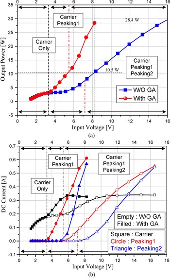
Fig. 11. The measured performances of the implemented 3-stage Doherty PA with and without the gate bias adaptation, (a) output power of the 3-stage Doherty PA and (b) DC currents of each PA versus input voltage.

Fig. 12. The measured CW characteristics of 3-stage Doherty PA. (a) DE, PAE, and gain performance without and (b) with the gate bias control, and (c) DC current characteristics.
C) Measured results for the modulation signal and linearization
Using the gate bias shaping functions shown in Fig. 10, the ET signals for each peaking PA are generated by the Matlab simulator. The generated signals are downloaded to Agilent's ESG4438C signal source and applied to the peaking PA's gate bias network through the gate driver circuit, which consists of the TI's THS3001 OP-Amp.
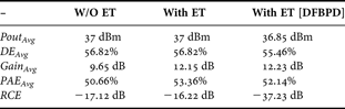
The measured AM–AM and AM–PM responses of the 3-stage Doherty PA with and without the ET technique are shown in Fig. 13. Owing to the large gain degradation of the 3-stage Doherty PA without the ET technique, it has a highly saturated curve on the AM–AM response. On the other hand, the proposed PA's AM–AM response is considerably linearized. However, the proposed PA as a even worse amplitude modulation–phase modulation (AM–PM) response because the gate bias control is not optimized for linearity, but the load modulation behavior for the flat gain response and peak power. To linearize the proposed PA, the digital feedback predistortion (DFBPD) has been applied to the RF input signal and the gate bias [Reference Woo1], as shown in Fig. 14. The linearized AM–AM and AM–PM responses of the proposed 3-stage Doherty PA are shown in Fig. 15, and the output spectra before and after the linearization for the WiMAX signal with the 8.5 dB PAPR are presented in Fig. 16. By employing the DFBPD algorithm, the adjacent channel leakage ratio (ACLR) at the 3.572-MHz offset is linearized to −39.8 dBc, and the performance is summarized in Table 4. Comparing the PAs with and without the ET, the PAE characteristic of the proposed 3-stage Doherty PA is improved by about 2.7% with the 2.5 dB-enhanced gain at the same average output power of 37 dBm. After linearization, the proposed PA has 52.14% and 55.46% of high PAE and DE, respectively, at an average output power of 36.85 dBm which is a 7.7 dB backed-off output power level from the peak power. The relative constellation error (RCE) is also enhanced to −37.23 dB, successfully satisfying the system specification. The constellation diagrams before and after the linearization of the proposed 3-stage Doherty PA are shown on Fig. 17. These experimental results clearly show that the proposed 3-stage Doherty PA with the ET technique has a high efficiency with high peak power, and it is suitable for a linear transmitter.

Fig. 13. Measured AM–AM and AM–PM characteristics of the 3-stage Doherty PA with and without the ET technique: (a) AM–AM, and (b) AM–PM

Fig. 14. The DFBPD algorithm for the ET 3-stage Doherty PA

Fig. 15. Measured AM–AM and AM–PM characteristics of the 3-stage Doherty PA after linearization: (a) AM–AM, and (b) AM–PM

Fig. 16. Measured output spectrum of the ET 3-stage Doherty PA before and after the linearization at an average output power of 37 dBm

Fig. 17. Measured signal constellation diagrams of the ET 3-stage Doherty PA, before (left) and after (right) linearization.
Table 4. The measured average performances of the 3-stage Doherty PA with and without the gate bias control for the 802.16e Mobile WiMAX signal with 8.5 dB PAPR.
V. Conclusions
We have suggested an optimized 3-stage Doherty PA with the ET technique to achieve the high peak power and maximum efficiency at the backed-off output power region. It is verified through Matlab simulation for the operational behavior of the PA that the 3-stage Doherty PA has the best flat efficiency versus the output power level among the various Doherty architecture. However, we have found that the PA has a seriously improper load modulation, and the proper load modulation behavior can be achieved by applying the gate bias control technique. For verification, 5 W and 10 W PEP LDMOSFETs have been used for the unit PA at 1-GHz, which is a class F−1 to maximize the efficiency of the PA. In the experiment, the gate bias adaptation is optimized for the accurate and maximally efficient Doherty operation. The proposed 3-stage Doherty PA has improved the gain and PAE by 2.5 dB and 2.7%, respectively, at the same average output power of 37 dBm by employing the ET technique. After the linearization, the proposed PA shows 52.14% and 55.46% of PAE and DE characteristics, respectively, at an average output power of 36.85 dBm, a 7.7 dB backed-off output power level. The RCE is −37.23 dB, satisfying the system specification. Therefore, it is clearly verified that the ET 3-stage Doherty PA using the saturated PA is a very powerful architecture for high efficiency, and the proposed gate bias control method employing ET technique is essential for the proper load modulation behavior. This architecture is suitable for the highly efficient and linear transmitter.
ACKNOWLEDGMENTS
This research was supported by the MKE (The Ministry of Knowledge Economy), Korea, under the ITRC (Information Technology Research Center) support program supervised by the NIPA (National IT Industry Promotion Agency)" (NIPA-2010-(C1090-1011-0011)), by the WCU (World Class University) program through the Korea Science and Engineering Foundation funded by the Ministry of Education, Science and Technology (Project No. R31-2008-000-10100-0).
 Ildu Kim received the B.S. degree in electronics and information engineering from Chon-nam National University, Kwangju, Korea, in 2004. He is currently working toward the Ph.D. degree in Pohang University of Science and Technology (POSTECH), Pohang, Korea. His current research interests include highly linear and efficient RF power amplifier design, linear power amplifier (LPA) system design and highly linear and efficient RF transmitter architectures.
 Junghwan Moon received the B.S. degree in electrical and computer engineering from University of Seoul, Seoul, Korea, in 2006, and is currently working toward the Ph.D. degree at the Pohang University of Science and Technology (POSTECH), Pohang, Gyungbuk, Korea. His current research interests include highly linear and efficient RF PA design, memory-effect compensation techniques and digital predistortion (DPD) techniques.
 Jungjoon Kim received the B.S. degree in electrical engineering from Han-Yang University, Ansan, Korea, in 2007, and the Master degree in electrical engineering from the Pohang University of Science and Technology (POSTECH), Pohang, Gyeongbuk, Korea, in 2009. He is currently working toward the Ph.D. degree at the POSTECH, Pohang, Gyeongbuk, Korea. His current research interests include the RF PA design and supply modulator design for a highly efficient transmitter system.
 Seunghoon Jee received the B.S. degree in electronic and electrical engineering from Kyungpook National University, Daegu, Korea, in 2009 and is currently working toward the Ph.D. degree at the Pohang University of Science and Technology (POSTECH), Pohang, Korea. His current research interests include highly linear and efficient RF PA design.
 Junghwan Son received the B.S. degree in physics from Sejong University, Seoul, Korea, in 2008, and received the M.S. degree in computer and communications engineering from the Pohang University of Science and Technology (POSTECH), Gyeongbuk, Pohang, Korea, in 2010, and currently working toward the Ph.D. degree in electrical and electronics engineering at the POSTECH. His current research interests include the RF PA design and linearity.
 Bumman Kim (M'78-SM'97-F'07) received the Ph.D. degree in electrical engineering from Carnegie Mellon University, Pittsburgh, PA, in 1979. From 1978 to 1981, he was engaged in fiber-optic network component research with GTE Laboratories Inc. In 1981, he joined the Central Research Laboratories, Texas Instruments Incorporated, where he was involved in development of GaAs power field-effect transistors (FETs) and monolithic microwave integrated circuits (MMICs). He has developed a large-signal model of a power FET, dual-gate FETs for gain control, high-power distributed amplifiers, and various millimeter-wave MMICs. In 1989, he joined the Pohang University of Science and Technology (POSTECH), Pohang, Gyungbuk, Korea, where he is a Namko Professor with the Department of Electrical Engineering, and Director of the Microwave Application Research Center, where he is involved in device and circuit technology for RF integrated circuits (RFICs). He was a Visiting Professor of electrical engineering at the California Institute of Technology, Pasadena, in 2001. He has authored over 200 technical papers. Dr Kim is a member of the Korean Academy of Science and Technology and the Academy of Engineering of Korea. He was an associate editor for the IEEE TRANSACTIONS ON MICROWAVE THEORY AND TECHNIQUES and a Distinguished Lecturer of the IEEE Microwave Theory and Techniques Society (IEEE MTT-S).


