I. INTRODUCTION
Rapid development in multi-band and/or multi-service wireless communication systems has been attracted more attention. Therefore, the realization of compact and high-performance multi-band components has become a key trend in the field of research, such as the applications of Global System for Mobile Communications (GSM) and Wireless Local Area Network (WLAN). Therefore, multi-passband filters became important building blocks and deeply demanded. To design a multi-band filter with low insertion loss, compact size, good passband selectivity, and wide stopband is a challenge for the circuit designers.
Only few methods for quad-band bandpass filters (BPFs) were reported [Reference Cheng and Yang1–Reference Ren4]. In [Reference Cheng and Yang1], four kinds of basic structures (outer-frame, U-shaped resonator, modified end-coupled microstrip line, and defected ground structures (DGSs)) were combined to develop a miniature quad-band BPF on a ceramic substrate. However, the passbands cannot implement individually and hard to determine the bandwidth as each passband. In [Reference Liu, Wang, Zeng and Chang2], the quad-band filter using CPW-fed dual-mode double-square ring resonators was proposed. Resonant frequencies can be controlled by tuning the perimeter ratio of the square rings. However, large circuit size and complexity in design have become problematic issues. In [Reference Wu and Yang3], the filter only employs two sets of the asymmetric Stepped impedance resonator (SIRs). One set is designed to operate at the first and third passbands (2.4/5.2 GHz) and the other set is employed at second and fourth passbands (3.5/6.8 GHz). However, the cost of the circuit size can be further improved. In [Reference Ren4], the filter composed of both a microstrip and a DGS slot is employed to obtain quad-frequency responses. However, the DGSs may disturb the current distributions on the ground plane to increase the microwave losses of the filter. Multi-layered fabrications have been widely used for the low-temperature cofired ceramic (LTCC) technologies [Reference Tang and Hsu5]. There are three advantages of the filters using multi-layered fabrication, such as strong couplings between the resonators can be achieved, cross-coupling effects can be easily introduced between the resonators to improve the passband selectivity of the filter, and the overall circuit size can be further reduced, compared with the conventional single-layered filter under the same frequency response.
In this paper, we propose a new quad-band filter using multi-mode resonators based on multi-layered substrate technique. The filter consists of a pair of multi-mode resonators operated at 1.8/3.7 GHz on the top layer and the other pair of the multi-mode resonators operated at 2.4/3 GHz on the bottom layer. Using the combination of the coupled uniform impedance resonators (UIRs), SIRs, and the source–load coupling lines, the quad-passbands with very close and having the high in-band isolation (≈30 dB) were well achieved. The filter has compact circuit size and strong design feasibility since the arrangement of the resonators and the quad-passbands can be easily determined by properly tuning the dimension of the resonators. The proposed filter is designed at 1.8/2.4/3/3.7 GHz. This study provides a simple and effective method to design a low-loss compact quad-passband filter without complex design and fabrication process.
II. FILTER DESIGN
Figure 1 shows the top layer view, bottom layer view, and coupling structure of the proposed filter. The filter consists of a pair of multi-mode resonators (UIR and SIR) on top layer operated at 1.8/3.7 GHz and the other pair of the multi-mode resonators on bottom layer operated at 2.4/3 GHz. Source–load coupling lines are used to be the input/output (I/O) ports for providing the multi-paths propagations by cross-coupling effects in the filter. The coupling strength between the I/O ports can be varied by tuning the length of the folded source–load lines. Each passband can be implemented individually, while each of the coupling coefficients between adjacent resonators can be extracted separately at the specific passbands. The multi-layered filter could not only save the circuit size but also generate the cross coupling effects, which the transmissions zeroes near the passband edges can be easily achieved. The coupling structure is similar to that in [Reference Wu, Chen and Chen6], as shown in Fig. 1(c).

Fig. 1. (a) Top layer view, (b) bottom layer view, and (c) coupling structure of the proposed filter (thickness of the substrate is h = 0.787 mm, resonators 1 and 2 are indicated by red solid marking on top layer, and resonators 3, 4, and source–load lines are indicated by blue solid marking on bottom layer).
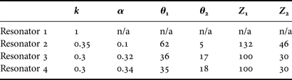
Figure 2(a) shows the structure of the SIR with impedance ratio K = Z 2/Z 1 < 1 and length ratio α = θ 2/(θ 1 + θ 2). The impedance ratio and physical length of SIRs are adjusted to meet the fundamental resonances (f 0) and the first spurious frequencies (f S1) over a wide frequency range. The resonance conditions are determined by Kcotθ 2 = tanθ 1 (odd mode) and Kcotθ 2 = −cotθ 1 (even mode) [Reference Makimoto and Yamashita7]. When the θ 2 is proportional to the physical length of SIR, the length ratio α of the SIR is defined as α = θ 2/(θ 1 + θ 2) = 2θ 2/θ t (θ t = 2θ 1 + 2θ 2); therefore, the equations of Kcot (αθ t/2) = tan [(θ t–αθ t)/2] and Kcot (αθ t/2) = −cot [(θ t–αθ t)/2] are found to determine every resonant frequencies of the SIR. The relations between the normalized f S1/f 0 versus length ratio α with impedance ratio K = 0.25 to 1 are shown in Fig. 2(b). The curves would be very useful for achieving the desired passbands of the filter without influencing each other. The marked points of A, B, and C are chosen for the optimal design parameter in this work. The dimensions of each resonator are summarized in Table 1.
Fig. 2. (a) Structure of the SIR with K = Z 2/Z 1 < 1 and α = θ 2/(θ 1 + θ 2) and (b) the relations between the normalized f S1/f 0 versus length ratio α with impedance ratio K = 0.25–1.
Table 1. Parameters of the proposed filter.

Recently, stub-loaded resonators are one of new structure for developing the triple-passband filters [Reference Chen, Weng and Chang8]. Using the UIRs and the SIRs with stub-loaded structures, the design freedom is limited when choosing every passband frequency position. However, circuit size is also an issue and should be further improved, especially the specific of first passband have to design at lower frequency band (≤2 GHz). Figure 3(a) shows the simulated frequency responses of the resonant peaks under different lengths for the resonator 3 with open-circuited stub in this work. When the R 1 is increased to 31 mm, the frequency of first passband could be moved to 1.8 GHz; however, the structure would cost a larger circuit size and increasing the microwave loss. Therefore, the modified resonator using the short-circuited stub can overcome this issue to maintain the circuit size as original ones, as shown in Fig. 3(b). The frequency of first passband can be moved from 1.6 to 1.9 GHz by changing the D 1 from 2.5 to 4.5 mm at radius of the via hole setting as 0.5 mm. The resonator using short-circuited stub can be effective reduced the circuit size to about 90% as compared with the resonator using open-circuited stub. Figure 3(c) shows the resonant peaks under different radius of via holes for the resonator using the shorted-circuit stub. By changing the radius of via hole, the frequency of first passband can be changed but the frequency of second passband was maintained. Each resonant path can be easily controlled to very close or far away the passbands for high design freedom.
Fig. 3. Simulated frequency responses of (a) the resonant peaks under different lengths for the resonator 3 with open-circuited stub, (b) the resonant peaks under different dimensions of D 1, and (c) the resonant peaks under different radius of via holes for the resonator 3 with shorted-circuit stub.
Figure 4 shows the relations between the 3-dB fractional bandwidth (FBW) and the coupling gap of S 1 at 1.8/2.4 and 3/3.7 GHz of the proposed filter. The extraction of quality factor (Q e) can be found as follows [Reference Hong and Lancaster9]:
 $${Q_{ei}}={f_{0i}}/\lpar \Delta {f_{ \pm 90^{\circ} }}\rpar \comma \; \quad i=1\comma \; \, 2\comma \; \, 3\comma \; \; {\rm or}\; 4\comma \;$$
where f 0i and Δf ±90° represent the resonant frequency and the absolute bandwidth between the ±90° points of S 11 phase response for the coupling gap S 1 between the I/O ports. The subscript i indicates first passband to fourth passband. The subscript i is corresponding to the order of the filter shown in Fig. 1. The corresponding realizable 3-dB FBWs (Δi) for four passbands are as follows:
 $${\Delta _i}={g_{0i}}{g_{1i}}/{Q_{ei}}\quad i=1\comma \; \; 2\comma \; \; 3\comma \; \; {\rm or}\; 4\comma \;$$
where g 0i and g 1i represent the prototype low-pass filter circuit parameters and Q ei is the extracted external quality factor using the full-wave electromagnetic (EM) simulation [10]. Figure 5 shows the current distribution of the proposed quad-band filter. It is clearly observed that the quad-passbands at 1.8, 2.4, 3, and 3.7 GHz are generated by four resonant paths in the proposed structure, respectively, and no interactions are introduced between the resonators to interfere the performance of each passband.
Fig. 4. Relations between the FBW and the coupling gap S 1 at (a) 1.8/2.4 GHz and (b) 3/3.7 GHz for the proposed filter.
Fig. 5. Current distribution of the proposed quad-band filter.
III. RESULTS
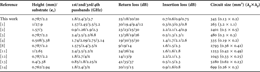
The Duroid 5880 substrate (ε r = 2.2, h = 0.787, and tan δ = 0.0009) is used for the filter fabrication. The overall size of the fabricated filter is 15 × 23 mm2, i.e., approximately 0.13 λ g by 0.2 λ g, where λ g is the guided wavelength at the center frequency of the first passband. The proposed filter was measured by an R&S ZVA40 vector network analyzer (VNA). Figure 6 shows the photograph and measured results of the filter. The filter has measured minimum insertion loss (−20log|S 21|) of 0.7, 0.6, 0.9, and 0.75 dB, maximum return loss (−20log|S 11|) are 25, 18, 20, and 20 dB corresponding to the passbands of 1.8, 2.4, 3, and 3.7 GHz, respectively. The 3-dB FBWs are 6.7, 8.2, 4.6, and 7.2%. The transmission zeros at each passband edge are clearly observed, resulting in high passband selectivity. The comparison of the proposed filter with other reported quad-band BPFs is summarized in Table 2. The multi-layered structure essentially helps not only to create the multi-path propagation, but also to reduce the overall circuit size.
Fig. 6. (a) Photograph and (b) measured results of the proposed filter.
Table 2. Comparisons with other proposed filters (λ g is the guided wavelength of the first center passband frequency).
IV. CONCLUSION
A compact quad-passband BPF using multi-layered technique based on multi-mode resonators is newly proposed. Using the combination of the coupled UIRs, SIRs, and the source–load coupling lines, the quad-passbands with very close and having the high in-band isolation (≈30 dB) were well achieved. There are three advantages of the proposed multi-layered filter, such as the strong couplings between the resonators can be achieved, cross-coupling effects can be easily introduced between the resonators to improve the passband selectivity of the filter and the overall circuit size can be further reduced, compared with the conventional single-layered filter under the same frequency response. Measured results reveal that the filter achieves a compact circuit size, low insertion loss, and good passband selectivity at each passband. The design procedure of the proposed filter is simple and may be followed easily.
ACKNOWLEDGEMENT
This work was supported by the NSC under Grant numbers NSC 102-2633-E-168-001 and NSC 102-2511-S-168-003.
 Hung-Wei Wu was born in Taipei, Taiwan on October 28, 1978. He received his Ph.D. degree from the Institute of Microelectronics, National Cheng Kung University, Taiwan in 2007. From October 2007, he joined the advanced optoelectronic technology center, National Cheng Kung University, Taiwan, where he is a Post-doctoral fellow. Now, he is an Associate Professor in the Department of Computer and Communication at Kun Shan University. He is the author and co-author of more than 90 papers in refereed journals and symposia proceedings. His research interests include the design of planar microwave filter, thin-film microstrip line, transparent conducting oxide (TCO) thin films, RF biosensor and modeling of the electromagnetic bandgap structure equivalent circuits in microwave, and millimeter-wave communication applications.
Shih-Hua Huang was born in Taipei, Taiwan on April 4, 1990. He received the M.S. degree in the Department of Computer and Communication, Kun Shan University, Tainan, Taiwan in 2013. He is the author and co-author of more than five papers in refereed journals and symposia proceedings. His research interests include analysis and design of passive microwave-integrated circuits.