


I. INTRODUCTION
In this era, there is a great demand for mobile communication and integrated wireless digital devices with very high data transfer rates. Antennas required for these applications should have certain extraordinary features such as high gain, light weight, wide bandwidth, ease of integration with microwave circuits, compact in size, compatibility with microwave monolithic integrated circuits, etc. The microstrip patch antennas generally meet most of these requirements and hence, have better prospects than conventional antennas [Reference Gupta and Kumar1–Reference Singh4]. However, their use in certain systems is limited as the single microstrip patch antenna has relatively low gain and narrow bandwidth with low efficiency. A lot of studies have been published on performance improvement of patch antennas, some of which are: (i) use of large number of patch antennas in array configuration [Reference Islam and Karmakar5, Reference Kishore, Rajesh, Kumar and Srinivasulu6]; (ii) increasing the substrate thickness [Reference Kovitz and Samii7, Reference Manteghi8]; (iii) optimizing the impedance matching of microstrip patch antenna by use of shorting pins, plates, posts, etc. [Reference Row and Hua9, Reference Chow and Wan10]; (iv) using high-permittivity substrates [Reference Tang, Wong, Long, Xue and Lau11, Reference Fukusako and Nakano12]; (v) modifying the basic patch shape [Reference Sharma, Upadhyay and Parthasarathy13]; (vi) using multiple substrates [Reference Rao and Kumar14]; (vii) loading conventional patch antenna by artificial materials [Reference Mittra, Li and Yoo15–Reference Ihsan and Munir27], etc.
In [Reference Kovitz and Samii7], Kovitz and Samii used a thick substrate to enhance the bandwidth of the microstrip patch antenna. However, increase in substrate thickness results in excitation of surface waves. These surface waves are dissipated at the substrate edges, resulting in the reduction of antenna gain. Many researchers improved the antenna performance by the use of optimized impedance matching techniques. Row and Hua [Reference Row and Hua9] tuned the impedance of the antenna to 50 Ω by placing a short through a hole at an appropriate position. Though such methods are flexible, as they avoid the use of impedance transformers, the search of the appropriate position for placing the short is quite tough and time-consuming job. In [Reference Tang, Wong, Long, Xue and Lau11], Tang et al. enhanced the axial ratio bandwidth of the patch antenna by use of high-permittivity substrate. However, high-permittivity substrates lead to the loss of surface waves. The modification in the shape of the patch has also been explored by various researchers to enhance the performance of the antenna. Sharma et al. [Reference Sharma, Upadhyay and Parthasarathy13] removed the arcs of the circular patch antenna from different positions. This removal of the arcs resulted in the gain, bandwidth, and cross-polar-level improvement. Though such modifications are easy to implement, the decision of locating such modifications is a tedious job. A technique of using multiple substrates has also been used by various groups. Rao and Kumar [Reference Rao and Kumar14] have used a multilayer dielectric substrate for gain and bandwidth enhancement. However, great efforts are required to fabricate such structures.
In recent years, several configurations of loading the conventional patch antenna with dielectric slabs [Reference Mittra, Li and Yoo15], electromagnetic band gap (EBG) structures [Reference Errifi, Baghdad, Badri and Sahel16–Reference Attia and Ramahi18], highly reflective surfaces [Reference Foroozesh and Shafai19, Reference Juyal and Shafai20], and the most recently, artificial magnetic materials [Reference Joshi, Pattnaik and Devi21–Reference Ihsan and Munir27] have been reported by several researchers to uplift the performance parameters of the antennas and squeeze their size. Loading of a conventional patch antenna with EBGs, highly reflective surfaces, etc. by various research groups have resulted in the performance improvement of antenna parameters, but this method generally makes the antenna bulky and difficult to fabricate. For example, in [Reference Attia and Ramahi18], Attia and Ramahi used a cross-stacked EBG substrate, making the antenna bulky and difficult to fabricate. Foroozesh and Shafai, used a highly reflective frequency selective surface (FSS), consisting of 15 × 15 FSS unit cells, etched on a dielectric slab [Reference Foroozesh and Shafai19].
Recently, antenna researchers worldwide have been attracted by the single/double negative metamaterials, also called zero-index materials, due to their peculiar properties. These artificially engineered homogeneous media provides unusual and useful phenomenon due to their controllable electric and magnetic responses [Reference Lapine and Tretyakov28]. These artificial materials are characterized by either dispersion relations or by constitutive electromagnetic parameters. In 1968, Veselago, in his paper [Reference Veselago29], first time gave the theoretical explanation on materials with simultaneously negative permittivity and permeability and also predicted some peculiar phenomenon obtained from these metamaterials. After a long time in the 1990s, Pendry et al. demonstrated electric plasma (negative permittivity) from wire structures [Reference Pendry, Holden, Stewart and Youngs30] and then magnetic plasma (negative permeability) from ring-shaped structures [Reference Pendry, Holden, Robbins and Stewart31]. In [Reference Smith, Padilla, Vier, Nasser and Schultz32] Smith et al. were the first to experimentally demonstrate the double negative materials. Due to the novel properties of metamaterials, they have been deeply studied as a potential artificial material for a large number of applications in microwave and optical region [Reference Engheta and Ziolkowski33, Reference Alu, Engheta, Erentok and Ziolkowski34].
Recently, researchers are extensively using these materials since their novel properties are capable not only to squeeze the size of the antenna, but also improve its performance parameters such as return loss, voltage standing wave ratio (VSWR), bandwidth, gain, and directivity. Also, they have easy physical realization and can be comfortably incorporated with conventional antennas as compared with other engineered materials. Several configurations of metamaterial have been used by different research groups [Reference Joshi, Pattnaik and Devi21–Reference Ihsan and Munir27]. In [Reference Joshi, Pattnaik and Devi22], Joshi et al. deigned an multiple split ring resonator (MSRR) loaded dual-band microstrip patch antenna to obtain the size reduction. In [Reference Arora, Pattnaik and Baral23], Arora et al. loaded the conventional patch antenna with a split ring resonator, as a result of which significant improvement in gain and bandwidth is obtained. In another attempt, Arora et al. in [Reference Arora, Pattnaik and Baral24], etched a pair of split ring resonator on the ground plane of a conventional patch antenna array and observed the drastic improvement in its performance.
Since long back superstrate layers or cover layers are also used to increase the directivity of microstrip antennas, with Jackson and Alexopoulos, as the first group to make its use in 1985 [Reference Jackson and Alexopoulos35]. Since then several types of superstrate layers have been incorporated with patch antennas. In 2005, Burokur et al. investigated the effect of left-handed metamaterial (LHM) superstrate on the circular patch antenna [Reference Burokur, Latrach and Toutain36]. In [Reference Chaimool, Chung and Akkaraekthalin37], Chaimool et al. used metamaterial reflective surface for simultaneous gain and bandwidth enhancement of microstrip patch antenna. Li et al. in [Reference Li, Szabo, Qing, Li and Chen38], designed a high-gain antenna using a three-layer metamaterial superstrate.
As per the literature review done by the authors, most researchers have focused on the performance enhancement of the single-patch antenna covered with superstrate layer. No much research has been done toward the simultaneous enhancement of the gain and bandwidth of the microstrip patch antenna arrays using a single-layer, 2D (two-dimensional) planar metamaterial superstrate and their equivalent circuit analysis. To the best knowledge of the authors they, in [Reference Arora, Pattnaik and Baral25], first time used a square split ring resonator, for simultaneous gain and bandwidth enhancement of microstrip patch antenna array. The patches of the conventional patch antenna array were covered with this metamaterial superstrate layer. The proposed antenna array presented the drastic improvements in bandwidth and gain, simultaneously.
Extending the work of [Reference Arora, Pattnaik and Baral25], in this paper, the authors further improved the performance of conventional microstrip patch antenna array by loading it with a LHM, which is designed by a pair of circular split ring resonator and wire strip. Also, in this paper, authors have: (i) tested the loaded antenna array and validated the simulated and experimental results; (ii) theoretically analyzed the loaded antenna array; (iii) applied effective medium theory to the metamaterial unit cell; (iv) developed and discussed the equivalent circuit model of the composite structure. Such layers not only improve the performance of antennas, but are also helpful to protect the patch antenna from environmental hazards, especially when these antennas are placed on aircrafts and missiles. Patch antenna array, as well as metamaterial superstrate are designed using an FR-4 substrate and simulations are done using FEM (finite-element method)-based software HFSS and Mentor Graphics IE3D, a method of moment-based full-wave electromagnetic simulator.
II. METAMATERIAL SUPERSTRATE AND ANTENNA ARRAY DESIGN
Figure 1 depicts the geometrical structure of a two-element conventional microstrip patch antenna array and Fig. 2(a) presents the perspective view of conventional patch antenna array covered with the proposed metamaterial superstrate. Side view of the proposed antenna array is presented in Fig. 2(b). Both, conventional patch antenna array and metamaterial superstrate, are designed on the FR-4 substrate of thickness (t) = 1.48 mm, dielectric constant (ε r) = 4.3, and loss tangent = 0.01. The 50 Ω SMA coaxial connector is used to feed the antenna array. As calculated using the transmission line model equations [Reference Garg, Bhartia, Bhal and Ittipiboon39, Reference Balanis40], the length and width of microstrip patch are 11.95 and 15.88 mm, respectively. The overall dimensions of the ground plane are 52.5 mm × 67.10 mm. Various dimensions of the antenna array are presented in Table 1. As calculated from equations [Reference Garg, Bhartia, Bhal and Ittipiboon39, Reference Balanis40], the resonant input resistance of the rectangular patch antenna is 238.5 Ω. Edge feeding of the elements of the antenna array is done by using the corporate feed network. The center-to-center spacing between the two patches of the antenna array is 0.96 (λ g/2), where λ g represents the guided wavelength. The 109.2 Ω quarter wave transformer is used to match the rectangular patch with 50 Ω line.
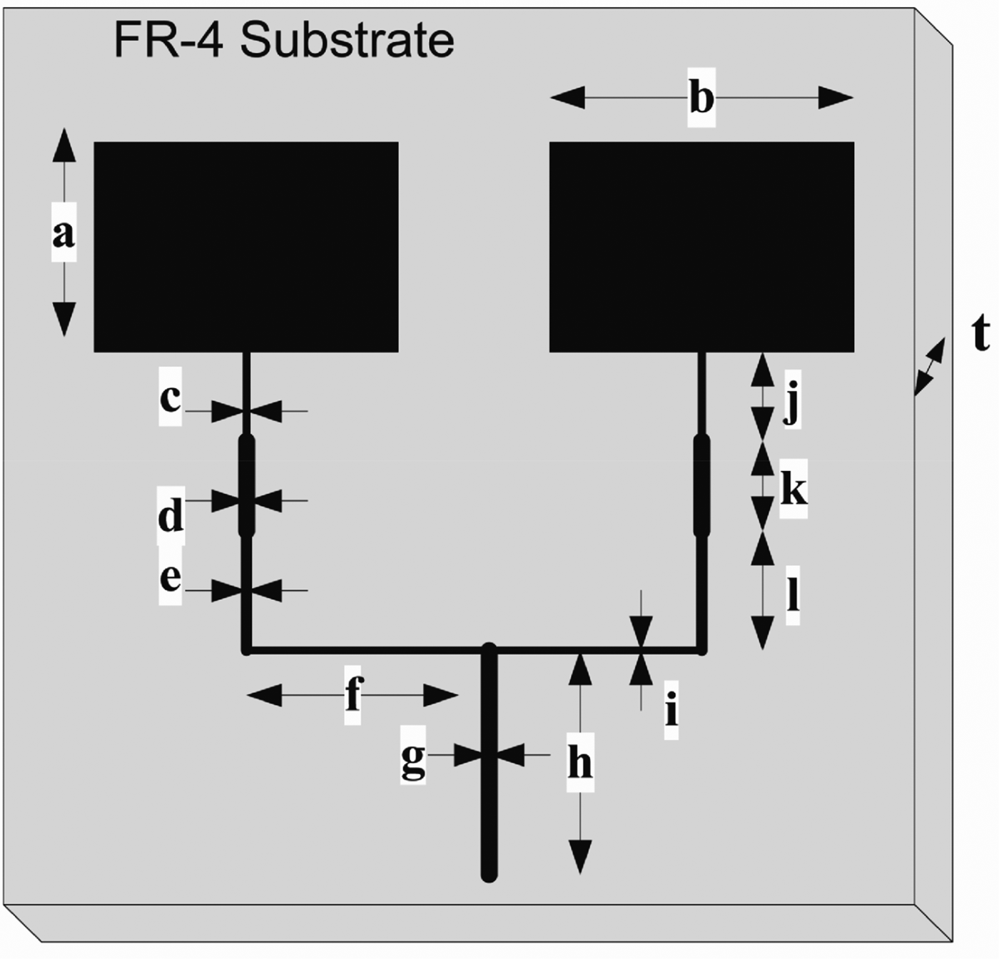
Fig. 1. Geometrical sketch of two-element conventional microstrip patch antenna array.
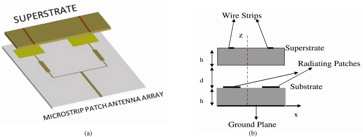
Fig. 2. Geometrical sketch of the proposed microstrip patch antenna array loaded with metamaterial superstrate: (a) perspective view, (b) side view.
Table 1. Dimensions of the antenna array.

As calculated from mathematical relations [Reference Pozar41], the width of the quarter wave transformer and 50 Ω transmission line is 0.5237 and 2.8758 mm, respectively. The length of the quarter wave transformer and 50 Ω line is calculated as 7.55 and 8 mm, respectively. Length of the feeding strip is calculated as 26 mm. The dimensions of the substrate are 52.5 mm × 67.1 mm. Figure 3 presents the structure of the circular split ring resonator unit cell and the geometric sketch of the double-negative metamaterial superstrate, consisting of a pair of this circular split ring resonator on the one side of FR-4 and copper wire etched on its opposite side, is depicted in Fig. 4.

Fig. 3. Geometrical structure of the circular split ring resonator unit cell.

Fig. 4. Top view of the proposed metamaterial superstrate.
The designed metamaterial superstrate is used to cover the patches of the conventional antenna array in such a way that it does not increase the overall size of the proposed antenna array, that is, the dimensions of loaded as well as unloaded antenna array remain almost same. The geometrical dimensions of the circular split ring resonator unit cell are; radius of the outer split ring (R) = 5.20 mm, width of the rings (w) = 0.2 mm, gap at the split of rings (g) = 0.2 mm, and separation between inner and outer split rings (s) is set to 1 mm. The dimensions of circular split ring resonator are chosen in such a way that it resonates at the same frequency as that of the patch antenna array. The center-to-center spacing between two circular split ring resonators is fixed at 17.50 mm. The length and width of each copper wire are 19 and 0.5 mm, respectively. This wire is etched on the opposite side of each circular split ring resonator in such a way that it passes through the center of each circular split ring resonator and distance between these two wires is fixed at 17.50 mm. This wire strip acts as a plasmon, thus exhibiting high-pass behavior for an incoming wave whose electric field is parallel to the wires and provides an effective negative permittivity below the plasma frequency. The overall dimension of the metamaterial superstrate layer is 52.5 mm × 19 mm and is placed at a distance (d) of 8 mm from the ground plane of the conventional patch antenna array. This distance of the superstrate layer, from the ground plane of the conventional patch antenna array, is found to be the optimum position for the best performance of the proposed array. Figure 5 presents the perspective view of the fabricated loaded antenna array.
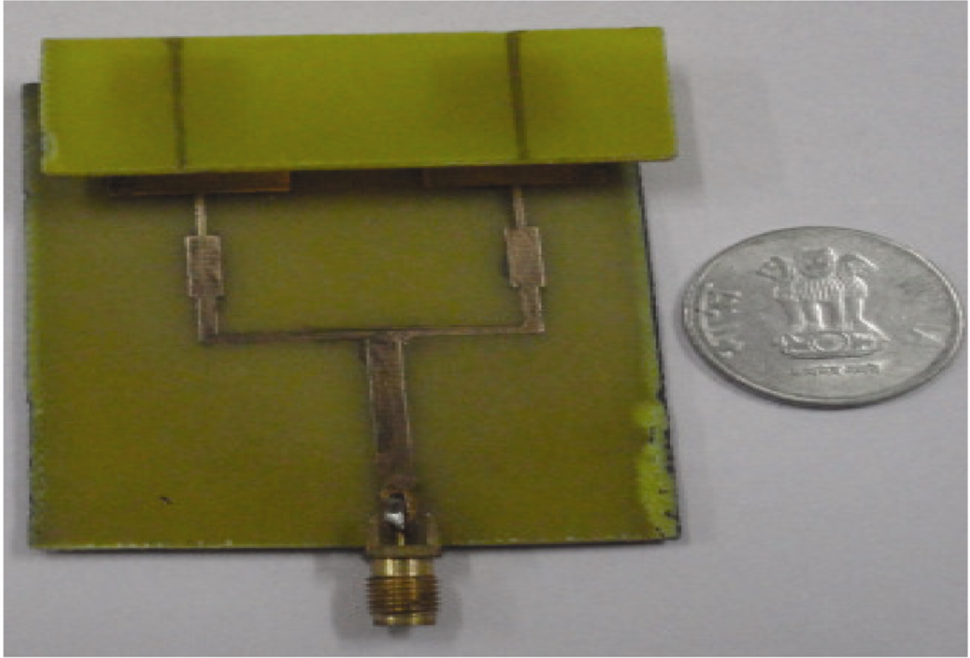
Fig. 5. Photograph of a fabricated metamaterial superstrate-loaded microstrip patch antenna array (perspective view).
III. RESULTS AND DISCUSSION
This section presents the simulated and measured results of the antenna array with and without metamaterial superstrate. Figure 6(a) depicts the simulated return loss characteristics of the conventional microstrip patch antenna array and the proposed metamaterial loaded antenna array, whereas Fig. 6(b) presents simulated and measured S 11 characteristics of the proposed metamaterial superstrate-loaded antenna array. It is observed that the unloaded antenna array resonates at 5.8 GHz with a bandwidth of 425 MHz, whereas, when the patches of the conventional patch antenna array are covered with metamaterial superstrate bandwidth reaches to 685 MHz at the same resonant frequency, thus corresponding to the bandwidth improvement of 60%.

Fig. 6. Return loss characteristics of: (a) unloaded and loaded antenna array (simulated), (b) loaded antenna array (measured and simulated).
Figures 7(a) and 7(b) represent the simulated elevation plane radiation pattern characteristics of the unloaded and loaded antenna array, respectively. As observed from these, the antenna array resonates at 5.8 GHz with a gain of 4.3 dBi under unloaded conditions and when the same antenna array is covered with a metamaterial superstrate, gain approaches to 11.9 dBi. A deep decline in radiation pattern, showed in Fig. 7(a), occurs due to the excitation of spurious modes on patch conductor. However, under loaded conditions, the presence of metamaterial superstrate makes field distribution of the patch antenna more uniform, thus improving the overall gain of the proposed array, as represented in Fig. 7(b). The dimensions of the array under both the conditions are almost same. Thus, the bandwidth and gain have improved simultaneously at no extra hardware cost. Figure 8 presents an inset photograph of the experimental setup to measure the return loss characteristics of the fabricated metamaterial superstrate-loaded antenna array. Anritsu Vector Network Analyzer (model no. MS2028C), frequency range 5 KHz–20 GHz, is used to test this proposed antenna array. From Fig. 6(b), it is observed that the fabricated antenna array is resonating at 5.8 GHz with a bandwidth of about 600 MHz, showing that both the results are in good agreement with each other. However, some changes in the shape of two curves are due to the inaccuracy occurred while fabricating the proposed antenna array and the use of an FR-4 substrate, which is lossy in nature but quite cheap, and hence suitable for making such prototypes.
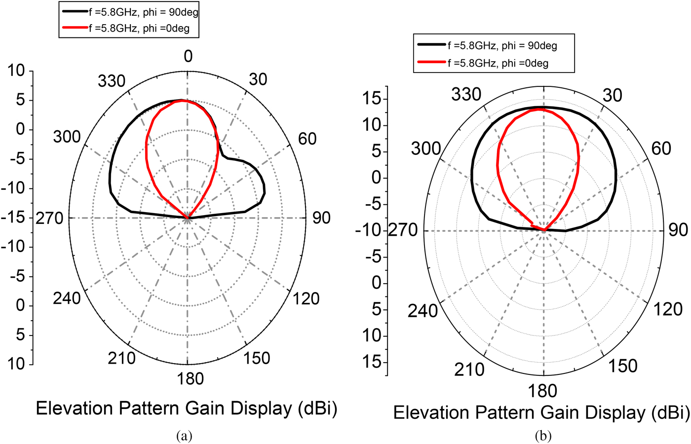
Fig. 7. Elevation plane radiation pattern characteristics of: (a) unloaded, (b) loaded proposed antenna array.

Fig. 8. Inset photograph of experimental setup to measure S 11 characteristics of fabricated metamaterial superstrate-loaded antenna array.
IV. METAMATERIAL UNIT CELL CHARACTERIZATION USING EFFECTIVE MEDIUM THEORY
To extract the effective constitutive parameters of the metamaterial unit cell, the sample is placed in a waveguide in such a way that the incident electromagnetic wave is polarized, with electric field along the axis of the wire strip and magnetic field parallel to the axis of circular split ring resonator. Hence, the direction of propagation of the wave vector k is along the z-axis. The arrangement of the sample inside the waveguide is shown in Fig. 9 and the S-parameters retrieved from it are presented in Fig. 10.

Fig. 9. Unit cell of metamaterial superstrate placed in a waveguide.
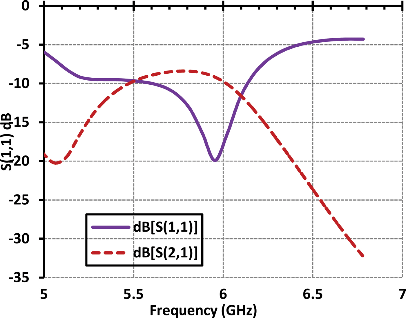
Fig. 10. S-parameters of metamaterial superstrate unit cell.
The NRW (Nicholson–Ross–Weir) technique [Reference Joshi, Pattnaik, Devi and Lohokare42] has been used to attain the effective magnetic permeability and electric permittivity of the metamaterial unit cell. The expressions of equations (1) and (2) are used to determine these effective medium parameters.
 $$\mu _r = \displaystyle{{\rm 2} \over {jk_od}}\displaystyle{{{\rm 1} - V_{\rm 2}} \over {{\rm 1} + V_{\rm 2}}},$$
 $$\varepsilon _r = \displaystyle{{\rm 2} \over {jk_od}}\displaystyle{{{\rm 1} - V_{\rm 1}} \over {{\rm 1} + V_{\rm 1}}},$$
where k 0 is the wave number, d is the thickness of the substrate; V 1 and V 2 are the composite terms to represent the addition and subtraction of S-parameters. The values of V 1 and V 2 are estimated using equations (3) and (4) [Reference Joshi, Pattnaik, Devi and Lohokare42].
 $$V_{\rm 1} = S_{{\rm 21}} +\, S_{{\rm 11}},$$
 $$V_{\rm 2} = S_{{\rm 21}} -\, S_{{\rm 11}}.$$
Using the obtained S-parameters, above mathematical equations, and MATLAB code, the magnetic permeability and electric permittivity characteristics of the proposed metamaterial unit cell are verified. From Figs 11(a) and 11(b) it is observed that the magnetic permeability and electric permittivity of the proposed metamaterial unit cell are negative from 5.7 to 6.0 GHz, implying that the structure exhibits metamaterial characteristics at the frequency of interest.
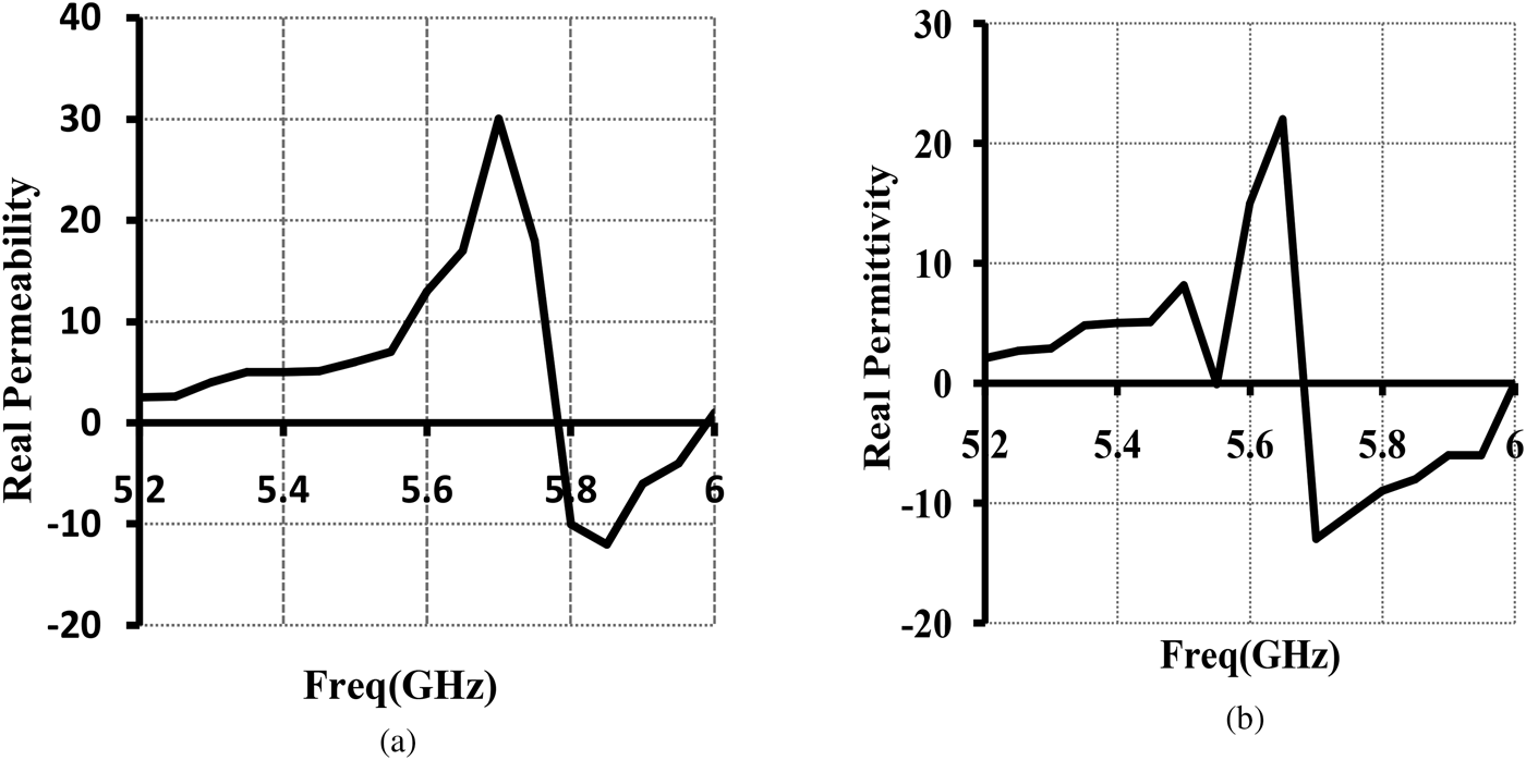
Fig. 11. Characteristics of the proposed metamaterial unit cell: (a) magnetic permeability curve, (b) electric permittivity curve.
V. EQUIVALENT CIRCUIT MODEL AND ANALYTICAL ANALYSIS
Placing the proposed metamaterial superstrate over the patches of the antenna array at small height results in the parasitic loading of the conventional patch antenna array. Due to this parasitic loading, proximity coupling between the superstrate and patch antenna occurs, thus forming a two-layer electromagnetically coupled system. This electromagnetic coupling between the patches and metamaterial superstrate, results in the improvement of the bandwidth of the composite system. Gain enhancement of the proposed antenna array can be explained with the help of cavity effect, which comes into existence when the superstrate layer forms the cover of the antenna patches. As per the Snell's Law of refraction, the medium with low refractive index moves the electromagnetic waves away from the primary source and in a direction which is parallel to the normal of this surface. This property results in the directivity enhancement of the proposed antenna array. The presence of metamaterial superstrate also makes the field distribution of the patch antenna more uniform, thus improving the overall gain of the proposed antenna array. Thus, it is concluded that the metamaterial superstrate acts as a parasitic load that enhances the bandwidth and the cavity effect improves the gain of the proposed antenna array. When the distance between the superstrate layer and the ground plane of the traditional antenna array is varied, the decrement in the gain improvement of the proposed metamaterial loaded antenna array is observed, as presented in Fig. 12.
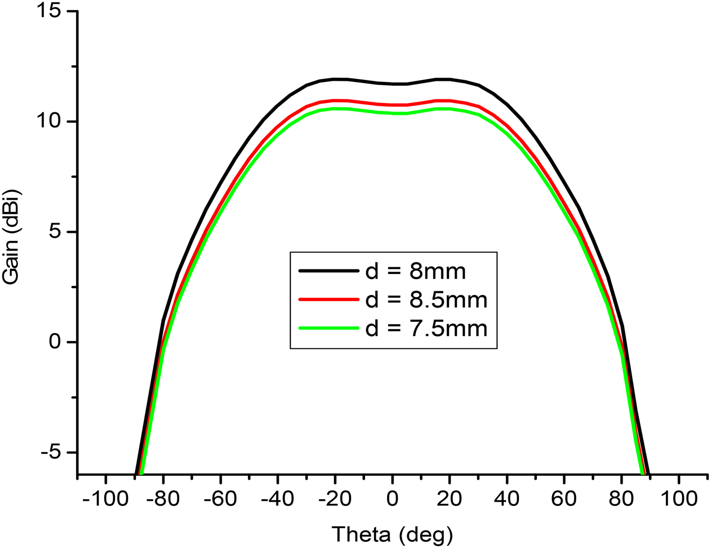
Fig. 12. Variation in the gain of the proposed antenna array as a function of distance (d) between the superstrate layer and the ground plane.
Figure 13 shows the equivalent circuit of microstrip patch antenna array loaded with a superstrate layer formed by circular split ring resonators and wire strips. The equivalent circuit model of the proposed superstrate layer is composed of the parallel connection between split ring resonator (SRR) and wire strip with a capacitor (C c). This capacitor represents the cross-coupling effect due to the wire strip etched on opposite face of the substrate. The patch antenna can be represented as a parallel RLC circuit the resistance, inductance and capacitance of which are represented by R 1, L 1, and C 1, respectively.

Fig. 13. Equivalent circuit of the proposed antenna array.
The wire strip etched on the back of circular split ring resonator can be modeled as an inductor, the inductance (L w), of which is given by equation (5) [Reference Mohan43]
 $$L_w = \displaystyle{{\mu _0l} \over {2\pi}} \left[ {\ln \left( {\displaystyle{{2l} \over w}} \right) + 0.5 + \left( {\displaystyle{w \over {3l}}} \right) - \left( {\displaystyle{{w^2} \over {24l^2}}} \right)} \right].$$
where l and w are length and width of the wire strip, respectively. Also, as per the principle of equivalent circuit theory, the modeling of the circular split ring resonator is done as an LC resonant circuit, such that the values of equivalent inductance of circular split ring resonator (L) and equivalent capacitance of circular split ring resonators (C) are calculated using equations (6) [Reference Terman44] and (7) [Reference Wang, Qu, Xu, Ma, Yang and Gu45], respectively.
 $$L = 0.00508\rho \left( {2.303{\log} _{10}\displaystyle{{4\rho} \over w} - \Upsilon} \right){\rm microhenry,}$$
where γ = 2.451, p is the total perimeter of the figure, and w is the width of the rings. The equivalent capacitance (C) of a circular split ring resonator is given as [Reference Wang, Qu, Xu, Ma, Yang and Gu45]
 $$C = (\pi C_P +\, C_S )/2,$$
where, C P = (2/π)rε0ln(2w/s) and C S = Aε0tw/g.
Such that r = 4 mm (radius of inner ring), A = 60, and t = 0.1 mm (thickness of metal sheet). Using equations (6) and (7), the calculated values of equivalent inductance (L) = 0.49 nH and equivalent capacitance (C) = 32.46 pF.
When the metamaterial superstrate is placed close to the patch, the circular split ring resonator gets inductively coupled with patch antenna due to which there exists some mutual inductance (M 1 and M 2) between them. This mutual inductance between circular split ring resonator and patch antenna is calculated using (8), the value of which is 1.11 nH.
 $$M_1 = M_2 = \displaystyle{{\mu _0L_s} \over {2\pi}} \left[ {0.467 + \displaystyle{{0.059{(w + W)}^2} \over {L_s^2}}} \right].$$
There also exists some mutual inductance between the neighboring circular split ring resonator (M 3) [Reference Labidi, Tahar and Choubani46] and neighboring patches (M 4) [Reference Mohan43], the magnitude of which are calculated using (9) and (10), respectively.
 $$M_3 = 4\pi \sqrt {a_1a_2\left[ {\left( {\displaystyle{2 \over k} - k} \right)F - \displaystyle{2 \over k}E} \right]}, $$
where, a 1 and a 2 are the radius of the inner and outer split rings, F and E are the complete elliptic integrals of the first and second kinds, respectively, to modulus k. Also
 $$k = \displaystyle{{2\sqrt {a_1a_2}} \over {{(a_1 + a_2)}^2 + l^2}}$$
where, l is the center-to-center distance between the two split ring resonators.
 $$M_4 = - \displaystyle{{\mu L} \over {2\pi}} \left[ {\ln (1 + \sqrt 2 ) + 1 - \sqrt 2 + w^2\sqrt 2 /24L^2} \right].$$
Due to the conducting nature of patches and split rings, they also possess some self-inductance. The self-inductance (M s) of the rectangular patch antenna is given by (11) [Reference Mohan43].
 $$M_s =\, \displaystyle{{\mu L} \over {{\rm 2}\pi}} \left[ {{\rm ln}\left( {\displaystyle{{{\rm 2}L} \over w}} \right) +\, 0{\rm. 5} +\, \displaystyle{w \over {{\rm 3}L}} - \displaystyle{{w^{\rm 2}} \over {{\rm 24}L^{\rm 2}}}} \right].$$
The inductance of microstrip patch antenna array with the capacitance of circular split ring resonator and the mutual inductances forms the LC resonant circuit of the loaded antenna array. This capacitance compensates the inductance of microstrip patch array and thus, under loaded conditions, good matching is obtained at the resonant frequency. L f represents the self-inductance of port and feeding network.
VI. CONCLUSIONS
Metamaterial superstrate-loaded microstrip patch antenna array for IEEE 802.16a 5.8 GHz Wi-MAX applications has been developed. The proposed composite structure enhances the gain of conventional patch antenna array by 7.6 dBi and bandwidth enhancement of 260 MHz is obtained, while maintaining the almost same profile and cost. The equivalent circuit of the proposed antenna array has been designed and analyzed. The proposed antenna array is fabricated and tested to support the simulated results. The performance comparison of the conventional unloaded antenna array and the proposed metamaterial superstrate-loaded antenna array show that the metamaterials have good potential to improve the performance of the antennas.
 Chirag Arora received his bachelor's degree in Electronics & Communication Engineering and Master's degree in communication from Panjab University Chandigarh, India. Presently he is working as assistant professor in KIET Group of Institutions, Ghaziabad, India and pursuing his doctorial degree from AKTU, Lucknow, India. Till date, he has fifteen research publications in national and international journals and conferences of repute. His area of specialization includes microwaves, antennas, communication and electromagnetics.
 Professor (Dr.) Shyam S. Pattnaik is Ph.D. in Engineering (Electronics & Telecommunication Engineering), M.Tech in Electronics & Communication Engineering and M.Sc. Physics (Electronics specialization). He has guided 57 master’s dissertations and 22 doctorial dissertations, out of which 05 are still in progress. Till date, he has 252 research publications in national and international journals and conferences of repute. He has carried out 07 projects and has done one invention disclosure. He has published two international books and three international book chapters. He has worked as Vice Chancellor, Biju Patnaik University of Technology, Rourkela, Govt. of Odisha, India for 2 years & 5 months. He has done 1½ years Post-Doctoral Research at University of Utah, USA. He has various awards and recognization to his credit, some of which are BOYSCAST Fellowship from DST, Govt. of India, SERC Visiting Fellowship, INSA Visiting Fellowship, UGC Visiting Fellowship, Distinguished Faculty Award, National Educational Excellence Award, National Scholarship, Best Paper Award, Listed in WHO’S WHO in the WORLD, Fellow of IETE, Life Member of ISTE, Senior Member of IEEE, USA. Research Associateship for Post-Doctoral Research from University of Utah, USA, Certificate of Commendation for Sponsored Project. Presently, he is working as Director, NITTTR, Chandigarh, India. His area of specialization includes Antenna Design and Analysis, Bio-Inspired Soft Computing, ICT enabled learning & teaching tools.
 Rudra Narayan Baral, was born in 1976, received his Bachelor's degree in 1998 from Institution of Electronics and Telecommunication Engineers, New Delhi. He got his Master's degree in Communication Systems in 2002 from MITS, Gwalior. He has done extensive research on planar components for high frequency applications leading to his PhD degree, awarded in 2010 from Rajiv Gandhi Technical University, Bhopal, Madhya Pradesh. Currently he is working as an associate professor in IMS Engineering College, Ghaziabad, India. Till date, he has a total of fifty two research publications of national and international repute. He is a life member of Institute of Electronics and Telecommunication Engineers (I.E.T.E.), New Delhi, India.


